
3-161
CAUTION: These devices are sensitive to electrostatic discharge; follow proper IC Handling Procedures.
1-888-INTERSIL or 321-724-7143
|
Copyright
©
Intersil Corporation 1999
HA-2544/883
Video Operational Amplifier
July 1994
File Number
511028-883
File Number
3699
Pinouts
HA-2544/883
(CERDIP)
TOP VIEW
HA-2544/883
(CLCC)
TOP VIEW
HA-2544/883
(METAL CAN)
TOP VIEW
1
2
3
4
8
7
6
5
NC
V+
OUT
BAL
+
BAL
-IN
+IN
V-
-
4
5
6
7
8
9
10 11 12 13
3
2
1
20 19
15
14
18
17
16
NC
BAL
NC
NC
NC
NC
V-
NC
BAL
NC
NC
V+
NC
OUT
NC
+
NC
-IN
NC
+IN
NC
-
NC
OUT
-IN
V -
BAL
+IN
V+
BAL
2
4
6
1
3
7
5
8
+
-
CASE TIED TO V-
Description
The HA-2544/883 is a fast, unity gain stable, monolithic op amp
designed to meet the needs required for accurate reproduction
of video or high speed signals. It offers high voltage gain
(3.5kV/V min, 6kV/V typ), wide unity gain bandwidth of 45MHz
minimum and phase margin of 65 degrees (open loop). Built
from high quality Dielectric Isolation, the HA-2544/883 is
another addition to the Intersil series of high speed, wideband
op amps, and offers true video performance combined with the
versatility of an op amp.
The primary features of the HA-2544/883, include wide band-
width, 150V/
µ
s (typ) slew rate, < 0.04dB differential gain error,
< 0.11 degrees differential phase error and gain flatness of
just 0.15dB at 3.58MHz and 4.43MHz, therefore proving to be
sufficient for video amplification. High performance and low
power requirements are met with a supply current of only
10mA typically and 12mA over the full temperature range.
Uses of the HA-2544/883 range from video test equipment
guidance systems, radar displays and other precise imaging
systems where stringent gain and phase requirements have
previously been met with costly hybrids and discrete circuitry.
The HA-2544/883 will also be used in non-video systems
requiring high speed signal conditioning such as data acquisi-
tion systems, medical electronics, specialized instrumentation
and communication systems.
Ordering Information
PART
NUMBER
TEMPERATURE
RANGE
PACKAGE
HA2-2544/883
-55
o
C to +125
o
C
8 Pin Can
HA4-2544/883
-55
o
C to +125
o
C
20 Lead Ceramic LCC
HA7-2544/883
-55
o
C to +125
o
C
8 Lead CerDIP
Features
∑ This Circuit is Processed in Accordance to MIL-STD-
883 and is Fully Conformant Under the Provisions of
Paragraph 1.2.1.
∑ Wide Unity Gain Bandwidth . . . . . . . . . . . 45MHz (Min)
∑ High Slew Rate . . . . . . . . . . . . . . . . . . . . . 100V/
µ
s (Min)
∑ Low Supply Current. . . . . . . . . . . . . . . . . . . 12mA (Max)
∑ Differential Gain Error . . . . . . . . . . . . . . . . 0.04dB (Max)
∑ Differential Phase Error. . . . . . . . . . . . . 0.11 Deg. (Max)
∑ Gain Flatness at 3.58MHz or 4.43MHz . . . 0.15dB (Max)
∑ Fast Settling Time (10V to 0.1%). . . . . . . . . 120ns (Typ)
Applications
∑ Video Systems
∑ Video Test Equipment
∑ Radar Displays
∑ Imaging Systems
∑ Pulse Amplifiers
∑ Signal Conditioning Circuits
∑ Data Acquisition Systems

3-162
Specifications HA-2544/883
Absolute Maximum Ratings
Thermal Information
Voltage Between V+ and V- Terminals . . . . . . . . . . . . . . . . . . . . 35V
Differential Input Voltage (Note 2) . . . . . . . . . . . . . . . . . . . . . . . . 6V
Voltage at Either Input Terminal . . . . . . . . . . . . . . . . . . . . . . V+ to V-
Peak Output Current (< 10% Duty Cycle) . . . . . . . . . . . . . . . . 40mA
Junction Temperature (T
J
) . . . . . . . . . . . . . . . . . . . . . . . . . . +175
o
C
Storage Temperature Range . . . . . . . . . . . . . . . . . -65
o
C to +150
o
C
ESD Rating. . . . . . . . . . . . . . . . . . . . . . . . . . . . . . . . . . . . . . <2000V
Lead Temperature (Soldering 10s) . . . . . . . . . . . . . . . . . . . . +300
o
C
Thermal Resistance
JA
JC
CerDIP Package . . . . . . . . . . . . . . . . . . .
115
o
C/W
28
o
C/W
Ceramic LCC Package . . . . . . . . . . . . . .
65
o
C/W
15
o
C/W
Metal Can Package . . . . . . . . . . . . . . . . .
155
o
C/W
67
o
C/W
Package Power Dissipation Limit at +75
o
C for T
J
+175
o
C
CerDIP Package . . . . . . . . . . . . . . . . . . . . . . . . . . . . . . . . 870mW
Ceramic LCC Package . . . . . . . . . . . . . . . . . . . . . . . . . . . . 1.54W
Metal Can Package . . . . . . . . . . . . . . . . . . . . . . . . . . . . . . 645mW
Package Power Dissipation Derating Factor Above +75
o
C
CerDIP Package . . . . . . . . . . . . . . . . . . . . . . . . . . . . . . 8.7mW/
o
C
Ceramic LCC Package . . . . . . . . . . . . . . . . . . . . . . . . 15.4mW/
o
C
Metal Can Package . . . . . . . . . . . . . . . . . . . . . . . . . . . . 6.5mW/
o
C
CAUTION: Stresses above those listed in "Absolute Maximum Ratings" may cause permanent damage to the device. This is a stress only rating and operation
of the device at these or any other conditions above those indicated in the operational sections of this specification is not implied.
Operating Conditions
Operating Temperature Range . . . . . . . . . . . . . . . . -55
o
C to +125
o
C
Operating Supply Voltage
. . . . . . . . . . . . . . . . . . . . . . . . . . . . . . . . ±
15V
V
INCM
1/2 (V+ - V-)
R
L
2k
TABLE 1. DC ELECTRICAL PERFORMANCE CHARACTERISTICS
Device Tested at: V
SUPPLY
=
±
15V, R
SOURCE
= 10
, R
LOAD
= 500k
, C
LOAD
10pF, V
OUT
= 0V, Unless Otherwise Specified.
PARAMETERS
SYMBOL
CONDITIONS
GROUP A
SUBGROUPS
TEMPERATURE
LIMITS
UNITS
MIN
MAX
Input Offset Voltage
V
IO
V
CM
= 0V
1
+25
o
C
-15
15
mV
2, 3
+125
o
C, -55
o
C
-20
20
mV
Input Bias Current
+I
B
V
CM
= 0V,
+R
S
= 1k
,
-R
S
= 10
1
+25
o
C
-15
15
µ
A
2, 3
+125
o
C, -55
o
C
-20
20
µ
A
-I
B
V
CM
= 0V,
+R
S
= 10
,
-R
S
= 1k
1
+25
o
C
-15
15
µ
A
2, 3
+125
o
C, -55
o
C
-20
20
µ
A
Input Offset Current
I
IO
V
CM
= 0V,
+R
S
= 1k
,
-R
S
= 1k
1
+25
o
C
-2
2
µ
A
2, 3
+125
o
C, -55
o
C
-3
3
µ
A
Common Mode
Range
+CMR
V+ = 5V, V- = -25V
1
+25
o
C
10
-
V
2, 3
+125
o
C, -55
o
C
10
-
V
-CMR
V+ = 25V, V- = -5V
1
+25
o
C
-
-10
V
2, 3
+125
o
C, -55
o
C
-
-10
V
Large Signal Voltage
Gain
+A
VOL
V
OUT
= 0V and +8V,
R
L
= 1k
4
+25
o
C
3.5
-
kV/V
5, 6
+125
o
C, -55
o
C
2.5
-
kV/V
-A
VOL
V
OUT
= 0V and -8V,
R
L
= 1k
4
+25
o
C
3.5
-
kV/V
5, 6
+125
o
C, -55
o
C
2.5
-
kV/V
Common Mode
Rejection Ratio
+CMRR
V
CM
= +10V,
V+ = +5V, V- = -25V,
V
OUT
= -10V
1
+25
o
C
75
-
dB
2, 3
+125
o
C, -55
o
C
75
-
dB
-CMRR
V
CM
= -10V,
V+ = +25V, V- = -5V,
V
OUT
= +10V
1
+25
o
C
75
-
dB
2, 3
+125
o
C, -55
o
C
75
-
dB
Output Voltage
Swing
+V
OUT
R
L
= 1k
1
+25
o
C
10
-
V
2, 3
+125
o
C, -55
o
C
10
-
V
-V
OUT
R
L
= 1k
1
+25
o
C
-
-10
V
2, 3
+125
o
C, -55
o
C
-
-10
V
Spec Number
511028-883

3-163
Spec Number
511028-883
Specifications HA-2544/883
Output Current
+I
OUT
V
OUT
= -9V
1
+25
o
C
25
-
mA
-I
OUT
V
OUT
= +9V
1
+25
o
C
-
-25
mA
Quiescent Power
Supply Current
+I
CC
V
OUT
= 0V, I
OUT
= 0mA
1
+25
o
C
-
12
mA
2, 3
+125
o
C, -55
o
C
-
12
mA
-I
CC
V
OUT
= 0V, I
OUT
= 0mA
1
+25
o
C
-12
-
mA
2, 3
+125
o
C, -55
o
C
-12
-
mA
Power Supply
Rejection Ratio
+PSRR
V
SUP
= 10V,
V+ = +10V, V- = -15V,
V+ = +20V, V- = -15V
1
+25
o
C
70
-
dB
2, 3
+125
o
C, -55
o
C
70
-
dB
-PSRR
V
SUP
= 10V,
V+ = +15V, V- = -10V,
V+ = +15V, V- = -20V
1
+25
o
C
70
-
dB
2, 3
+125
o
C, -55
o
C
70
-
dB
Offset Voltage
Adjustment
+V
IO
Adj
Note 1
1
+25
o
C
V
IO
-1
-
mV
-V
IO
Adj
Note 1
1
+25
o
C
V
IO
+1
-
mV
NOTE:
1. Offset adjustment range is [V
IO
(Measured)
±
1mV] minimum referred to output. This test is for functionality only to assure adjustment
through 0V.
2. To achieve optimum AC performance, the input stage was designed without protective diode clamps. Exceeding the maximum differential
input voltage results in reverse breakdown to the base-emitter junction of the input transistors and probable degradation of the input
parameters especially V
OS
, I
OS
and Noise.
TABLE 2. AC ELECTRICAL PERFORMANCE CHARACTERISTICS
Device Tested at: V
SUPPLY
=
±
15V, R
SOURCE
= 10
0
, R
LOAD
= 1k
, C
LOAD
= 10pF, V
OUT
= 1V/V, Unless Otherwise Specified.
PARAMETERS
SYMBOL
CONDITIONS
GROUP A
SUBGROUPS
TEMPERATURE
LIMITS
UNITS
MIN
MAX
Slew Rate
+SR
V
OUT
= -3V to +3V
7
+25
o
C
100
-
V/
µ
s
-SR
V
OUT
= +3V to -3V
7
+25
o
C
100
-
V/
µ
s
TABLE 3. ELECTRICAL PERFORMANCE CHARACTERISTICS
Device Characterized at: V
SUPPLY
=
±
15V, R
LOAD
= 1k
, C
LOAD
= 10pF, A
V
= 1V/V, Unless Otherwise Specified.
PARAMETERS
SYMBOL
CONDITIONS
NOTES
TEMPERATURE
LIMITS
UNITS
MIN
MAX
Differential Gain
dA
V
R
S
= 50
, R
L
= 1k
,
f
O
= 3.58MHz and
4.43MHz
1, 5, 6, 8
+25
o
C
-
0.04
dB
Differential Phase
d
R
S
= 50
, R
L
= 1k
,
f
O
= 3.58MHz and
4.43MHz
1, 6, 8
+25
o
C
-
0.11
Degrees
Unity Gain Bandwidth
UGBW
V
O
= 200mV
RMS
,
f at -3dB
1
+25
o
C
45
-
MHz
Gain Flatness
A
V
V
O
= 200mV
RMS
,
f
O
= 5MHz
1, 6
+25
o
C
-0.15
0.15
dB
V
O
= 200mV
RMS
,
f
O
= 10MHz
1, 6
+25
o
C
-0.35
0.35
dB
TABLE 1. DC ELECTRICAL PERFORMANCE CHARACTERISTICS (Continued)
Device Tested at: V
SUPPLY
=
±
15V, R
SOURCE
= 10
, R
LOAD
= 500k
, C
LOAD
10pF, V
OUT
= 0V, Unless Otherwise Specified.
PARAMETERS
SYMBOL
CONDITIONS
GROUP A
SUBGROUPS
TEMPERATURE
LIMITS
UNITS
MIN
MAX

3-164
Spec Number
511028-883
Specifications HA-2544/883
Full Power Bandwidth
FPBW
V
PEAK
= 1V
1, 2
+25
o
C
15.9
-
MHz
V
PEAK
= 5V
1, 2
+25
o
C
3.2
-
MHz
Minimum Closed Loop
Stable Gain
CLSG
R
L
= 1k
, C
L
1pF
1
-55
o
C to +125
o
C
1
-
V/V
Rise and Fall Time
T
R
V
OUT
= 0V to +200mV
1, 4
+25
o
C
-
15
ns
T
F
V
OUT
= 0V to -200mV
1, 4
+25
o
C
-
15
ns
Overshoot
+OS
V
OUT
= 0V to +200mV
1
+25
o
C
-
20
%
-OS
V
OUT
= 0V to -200mV
1
+25
o
C
-
20
%
Settling Time
T
S
Open Loop
1
+25
o
C
-
150
%
Output Resistance
R
OUT
Open Loop
1
+25
o
C
-
40
Quiescent Power
Consumption
PC
V
OUT
= 0V, I
OUT
= 0mA
1, 3
-55
o
C to +125
o
C
-
360
mW
NOTES:
1. Parameters listed in Table 3 are controlled via design or process parameters and are not directly tested at final production. These param-
eters are lab characterized upon initial design release, or upon design changes. These parameters are guaranteed by characterization
based upon data from multiple production runs which reflect lot to lot and within lot variation.
2. Full Power Bandwidth guarantee based on Slew Rate measurement using FPBW = Slew Rate/(2
V
PEAK
).
3. Quiescent Power Consumption based upon Quiescent Supply Current test maximum. (No load on outputs.)
4. Measured between 10% and 90% points.
5. A
D
(%) =
6. The video parameter specifications will degrade as the output load resistance decreases.
7. C-L Gain and C-L Delay were less than the resolution of the test equipment used which is 0.1dB and 7ns, respectively.
8. Test signal used is 200mV
RMS
at each frequency on a 0 and 1 volt offset. For adequate test repeatability, a minimum warm-up of 2 minutes
is suggested.
TABLE 4. ELECTRICAL TEST REQUIREMENTS
MIL-STD-883 TEST REQUIREMENTS
SUBGROUPS (SEE TABLES 1 AND 2)
Interim Electrical Parameters (Pre Burn-In)
1
Final Electrical Test Parameters
1 (Note 1), 2, 3, 4, 5, 6, 7
Group A Test Requirements
1, 2, 3, 4, 5, 6, 7
Groups C and D Endpoints
1
NOTE:
1. PDA applies to Subgroup 1 only.
TABLE 3. ELECTRICAL PERFORMANCE CHARACTERISTICS (Continued)
Device Characterized at: V
SUPPLY
=
±
15V, R
LOAD
= 1k
, C
LOAD
= 10pF, A
V
= 1V/V, Unless Otherwise Specified.
PARAMETERS
SYMBOL
CONDITIONS
NOTES
TEMPERATURE
LIMITS
UNITS
MIN
MAX
10
A
D
dB
(
)
20
-------------------------
-1
100
◊
3-165
All Intersil semiconductor products are manufactured, assembled and tested under ISO9000 quality systems certification.
Intersil products are sold by description only. Intersil Corporation reserves the right to make changes in circuit design and/or specifications at any time without
notice. Accordingly, the reader is cautioned to verify that data sheets are current before placing orders. Information furnished by Intersil is believed to be accurate
and reliable. However, no responsibility is assumed by Intersil or its subsidiaries for its use; nor for any infringements of patents or other rights of third parties which
may result from its use. No license is granted by implication or otherwise under any patent or patent rights of Intersil or its subsidiaries.
For information regarding Intersil Corporation and its products, see web site http://www.intersil.com
HA-2544/883
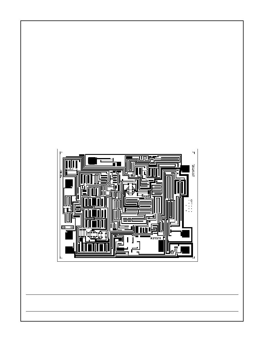
Die Characteristics
DIE DIMENSIONS:
80 x 64 x 19 mils
±
1 mils
2030 x 1630 x 483
µ
m
±
25.4
µ
m
METALLIZATION:
Type: Al, 1% Cu
Thickness: 16k
≈
±
2k
≈
GLASSIVATION:
Type: Nitride (Si3N4) over Silox (SIO2, 5% Phos.)
Silox Thickness: 12k
≈
±
2k
≈
Nitride Thickness: 3.5k
≈
±
1.5k
≈
WORST CASE CURRENT DENSITY:
7.0 x 10
4
A/cm
2
SUBSTRATE POTENTIAL (Powered Up): V-
TRANSISTOR COUNT: 44
PROCESS: Bipolar Dielectric Isolation
Metallization Mask Layout
HA-2544/883
V+
OUT
BAL
BAL
-IN
+IN
V-
Spec Number
511028-883