 | –≠–ª–µ–∫—Ç—Ä–æ–Ω–Ω—ã–π –∫–æ–º–ø–æ–Ω–µ–Ω—Ç: HA4404BCB | –°–∫–∞—á–∞—Ç—å:  PDF PDF  ZIP ZIP |
5
July 1998
HA4404B
330MHz, 4 x 1 Video
Crosspoint Switch with Tally Outputs
Features
∑ Low Power Dissipation . . . . . . . . . . . . . . . . . . . 105mW
∑ Symmetrical Slew Rates . . . . . . . . . . . . . . . . . 1250V/
µ
s
∑ 0.1dB Gain Flatness. . . . . . . . . . . . . . . . . . . . . . 165MHz
∑ -3dB Bandwidth . . . . . . . . . . . . . . . . . . . . . . . . . 330MHz
∑ Off Isolation (100MHz) . . . . . . . . . . . . . . . . . . . . . . 70dB
∑ Crosstalk Rejection (30MHz). . . . . . . . . . . . . . . . . 80dB
∑ Differential Gain and Phase . . . . . 0.01%/0.01 Degrees
∑ High ESD Rating . . . . . . . . . . . . . . . . . . . . . . . . >2000V
∑ TTL Compatible Control Inputs
∑ Open Collector Tally Outputs
∑ Improved Replacement for GX4404
Applications
∑ Professional Video Switching and Routing
∑ HDTV
∑ Computer Graphics
∑ RF Switching and Routing
Description
The HA4404B is a very wide bandwidth 4 x 1 crosspoint
switch ideal for professional video switching, HDTV, com-
puter monitor routing, and other high performance applica-
tions. The circuit features very low power dissipation
(105mW Enabled, 4mW Disabled), excellent differential gain
and phase, and very high off isolation. When disabled, the
output is switched to a high impedance state, making the
HA4404B ideal for routing matrix equipment.
The HA4404B requires no external current source, and fea-
tures fast switching and symmetric slew rates. The tally out-
puts are open collector PNP transistors to V+ to provide an
indication of crosspoint selection.
For a 4 x 1 crosspoint without Tally outputs or with synchro-
nous control signals, please refer to the HA4314B and
HA4344B Data Sheets, respectively.
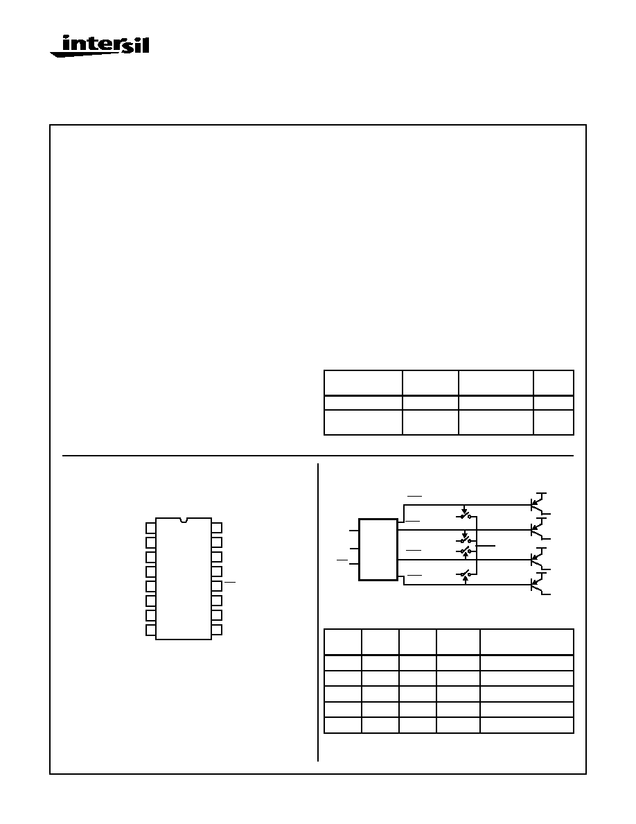
Pinout
HA4404B
(SOIC)
TOP VIEW
Functional Diagram
Ordering Information
PART NUMBER
TEMP.
RANGE (
o
C)
PACKAGE
PKG.
NO.
HA4404BCB
0 to 70
16 Ld SOIC
M16.15
HA4404BCB96
0 to 70
16 Ld SOIC Tape
and Reel
M16.15
14
15
16
9
13
12
11
10
1
2
3
4
5
7
6
8
IN0
GND
IN1
T1
T2
IN2
IN3
GND
T0
A0
A1
CS
OUT
V-
T3
V+
TRUTH TABLE
CS
A1
A0
OUT
ACTIVE TALLY
OUTPUT
0
0
0
IN0
T0
0
0
1
IN1
T1
0
1
0
IN2
T2
0
1
1
IN3
T3
1
X
X
High - Z
None, All High - Z
OUT
DECODE
EN0
EN1
EN2
EN3
IN0
IN1
IN2
IN3
A0
A1
CS
T0
V+
T1
V+
T2
V+
T3
V+
CAUTION: These devices are sensitive to electrostatic discharge. Users should follow proper IC Handling Procedures.
1-888-INTERSIL or 321-724-7143 | Copyright © Intersil Corporation 1999
File Number
3678.5

6
Absolute Maximum Ratings
Thermal Information
Voltage Between V+ and V- . . . . . . . . . . . . . . . . . . . . . . . . . . . . 12V
Input Voltage. . . . . . . . . . . . . . . . . . . . . . . . . . . . . . . . . . . . V
SUPPLY
Digital Input Current (Note 2) . . . . . . . . . . . . . . . . . . . . . . . .
±
25mA
Analog Input Current (Note 2) . . . . . . . . . . . . . . . . . . . . . . . .
±
5mA
Output Current . . . . . . . . . . . . . . . . . . . . . . . . . . . . . . . . . . . . 20mA
ESD Rating
Human Body Model (Per MIL-STD-883 Method 3015.7) . . 2000V
Operating Conditions
Temperature Range . . . . . . . . . . . . . . . . . . . . . . . . . . . 0
o
C to 70
o
C
Thermal Resistance (Typical, Note 1)
JA
(
o
C/W)
SOIC Package . . . . . . . . . . . . . . . . . . . . . . . . . . . . .
115
Maximum Junction Temperature (Die). . . . . . . . . . . . . . . . . . . 175
o
C
Maximum Junction Temperature (Plastic Package) . . . . . . . 150
o
C
Maximum Storage Temperature Range . . . . . . . . . -65
o
C to 150
o
C
Maximum Lead Temperature (Soldering 10s) . . . . . . . . . . . . 300
o
C
(SOIC - Lead Tips Only)
CAUTION: Stresses above those listed in "Absolute Maximum Ratings" may cause permanent damage to the device. This is a stress only rating and operation
of the device at these or any other conditions above those indicated in the operational sections of this specification is not implied.
NOTES:
5.
JA
is measured with the component mounted on an evaluation PC board in free air.
6. If an input signal is applied before the supplies are powered up, the input current must be limited to these maximum values.
Electrical Specifications
V
SUPPLY
=
±
5V, R
L
= 10k
, V
CS
= 0.8V, Unless Otherwise Specified
PARAMETER
TEST CONDITIONS
(NOTE 4)
TEMP. (
o
C)
MIN
TYP
MAX
UNITS
DC SUPPLY CHARACTERISTICS
Supply Voltage
Full
±
4.5
±
5.0
±
5.5
V
Supply Current (V
OUT
= 0V)
V
CS
= 0.8V
25, 70
-
10.5
13
mA
V
CS
= 0.8V
0
-
-
15.5
mA
V
CS
= 2.0V
25, 70
-
400
450
µ
A
V
CS
= 2.0V
0
-
400
580
µ
A
ANALOG DC CHARACTERISTICS
Output Voltage Swing without Clipping
V
OUT
= V
IN
±
V
IO
±
20mV
25, 70
±
2.7
±
2.8
-
V
0
±
2.4
±
2.5
-
V
Output Current
Full
15
20
-
mA
Input Bias Current
Full
-
30
50
µ
A
Output Offset Voltage
Full
-10
-
10
mV
Output Offset Voltage Drift (Note 3)
Full
-
25
50
µ
V/
o
C
SWITCHING CHARACTERISTICS
Turn-On Time
25
-
160
-
ns
Turn-Off Time
25
-
320
-
ns
Output Glitch During Switching
25
-
±
10
-
mV
DIGITAL DC CHARACTERISTICS
Input Logic Voltage
High
Full
2
-
-
V
Low
Full
-
-
0.8
V
Input Current
0V to 4V
Full
-2
-
2
µ
A
Tally Output High Voltage
I
OH
= 1mA
Full
4.7
4.8
-
V
Tally Off Leakage Current
V
TALLY
= 0V
Full
-20
-
20
µ
A
AC CHARACTERISTICS
Insertion Loss
1V
P-P
25
-
0.055
0.063
dB
Full
-
0.07
0.08
dB
Channel-to-Channel Insertion Loss Match
Full
-
±
0.004
±
0.006
dB
HA4404B

7
AC Test Circuit
NOTE:
C
L
= C
X
+ Test Fixture Capacitance.
PC Board Layout
The frequency response of this circuit depends greatly on
the care taken in designing the PC board. The use of low
inductance components such as chip resistors and chip
capacitors is strongly recommended, while a solid
ground plane is a must!
Attention should be given to decoupling the power supplies.
A large value (10
µ
F) tantalum in parallel with a small value
(0.1
µ
F) chip capacitor works well in most cases.
Keep input and output traces as short as possible, because
trace inductance and capacitance can easily become the
performance limiting items.
-3dB Bandwidth
R
S
= 50
, C
L
= 11pF
25
-
330
-
MHz
R
S
= 24
, C
L
= 19pF
25
-
290
-
MHz
R
S
= 15
, C
L
= 34pF
25
-
210
-
MHz
R
S
= 11
, C
L
= 49pF
25
-
170
-
MHz
±
0.1dB Flat Bandwidth
R
S
= 50
, C
L
= 11pF
25
-
165
-
MHz
R
S
= 24
, C
L
= 19pF
25
-
130
-
MHz
R
S
= 15
, C
L
= 34pF
25
-
137
-
MHz
R
S
= 11
, C
L
= 49pF
25
-
100
-
MHz
Input Resistance
Full
200
400
-
k
Input Capacitance
Full
-
1.5
-
pF
Enabled Output Resistance
Full
-
15
-
Disabled Output Capacitance
V
CS
= 2.0V
Full
-
2.5
-
pF
Differential Gain
4.43MHz, Note 3
25
-
0.01
0.02
%
Differential Phase
4.43MHz, Note 3
25
-
0.01
0.02
Degrees
Off Isolation
1V
P-P
, 100MHz, V
CS
= 2.0V,
R
L
= 10
Full
-
70
-
dB
Crosstalk Rejection
1V
P-P
, 30MHz
Full
-
80
-
dB
Slew Rate (1.5V
P-P
, +SR/-SR)
R
S
= 50
, C
L
= 11pF
25
-
1280/1260
-
V/
µ
s
R
S
= 24
, C
L
= 19pF
25
-
1190/1170
-
V/
µ
s
R
S
= 15
, C
L
= 34pF
25
-
960/930
-
V/
µ
s
R
S
= 11
, C
L
= 49pF
25
-
810/790
-
V/
µ
s
Total Harmonic Distortion
10MHz, R
L
= 1k
, Note 3
Full
-
0.01
0.1
%
Disabled Output Resistance
V
CS
= 2.0V
Full
-
12
-
M
NOTES:
7. This parameter is not tested. The limits are guaranteed based on lab characterization, and reflect lot-to-lot variation.
8. Units are 100% tested at 25
o
C; guaranteed, but not tested at 0
o
C and 70
o
C.
Electrical Specifications
V
SUPPLY
=
±
5V, R
L
= 10k
, V
CS
= 0.8V, Unless Otherwise Specified (Continued)
PARAMETER
TEST CONDITIONS
(NOTE 4)
TEMP. (
o
C)
MIN
TYP
MAX
UNITS
HA4404B
R
S
C
X
75
HFA1100
75
V
OUT
V
IN
10k
500
400
510
+
-
HA4404B

8
Application Information
General
The HA4404B is a 4 x 1 crosspoint switch that is ideal for the
matrix element of high performance switchers and routers.
This crosspoint's low input capacitance and high input resis-
tance provide excellent video terminations when used with
an external 75
resistor. Nevertheless, if several HA4404B
inputs are connected together, the use of an input buffer
should be considered (see Figure 1). This crosspoint con-
tains no feedback or gain setting resistors, so the output is a
true high impedance load when the IC is disabled (CS = 1).
Ground Connections
All GND pins are connected to a common point on the die,
so any one of them will suffice as the functional GND con-
nection. For the best isolation and crosstalk rejection, how-
ever, all GND pins must connect to the GND plane.
Frequency Response
Most applications utilizing the HA4404B require a series out-
put resistor, R
S
, to tune the response for the specific load
capacitance, C
L
, driven. Bandwidth and slew rate degrade
as C
L
increases (as shown in the Electrical Specification
table), so give careful consideration to component place-
ment to minimize trace length. In big matrix configurations
where C
L
is large, better frequency response is obtained by
cascading two levels of crosspoints in the case of multi-
plexed outputs (see Figure 2), or distributing the load
between two drivers if C
L
is due to bussing and subsequent
stage input capacitance.
Control Signals
CS - This is a TTL/CMOS compatible, active low Chip Select
input. When driven high, CS forces the output to a true high
impedance state and reduces the power dissipation by a fac-
tor of 25. The CS input has no on-chip pull-down resistor, so
it must be connected to a logic low (recommend GND) if the
enable function isn't utilized.
A0, A1 - These are binary coded, TTL/CMOS compatible
address inputs that select which one of the four inputs con-
nect to the crosspoint output.
T0-T3 - The Tally outputs are open collector PNP transistors
connected to V+. When CS = 0, the PNP transistor associ-
ated with the selected input is enabled and current is deliv-
ered to the load. When the crosspoint is disabled, or the
channel is unselected, the Tally output(s) present a very high
impedance to the external circuitry. Several Tally outputs
may be wire OR'd together to generate complex control sig-
nals, as shown in the application circuits below. The Tally
load may be terminated to GND or to V- as long as the con-
tinuous output current doesn't exceed 3mA (6mA at 50%
duty cycle, etc.).
Switcher/Router Applications
Figure 1 illustrates one possible implementation of a wide-
band, low power, 4 x 4 switcher/router utilizing the HA4404B
for the switch matrix. A 4 x 4 switcher/router allows any of
the four outputs to be driven by any one of the four inputs
(e.g., each of the four inputs may connect to a different out-
put, or an input may connect to multiple outputs). This appli-
cation utilizes the HA4600 (video buffer with output disable)
for the input buffer, the HA4404B as the switch matrix, and
the HFA1112 (programmable gain buffer) as the gain of two
output driver. Figure 2 details a 16 x 1 switcher (basically a
16:1 mux) which uses the HA4201 (1 x 1 crosspoint) and the
HA4404B in a cascaded stage configuration to minimize
capacitive loading at each output node, thus increasing sys-
tem bandwidth.
Power Up Considerations
No signals should be applied to the analog or digital inputs
before the power supplies are activated. Latch-up may occur
if the inputs are driven at the time of power up. To prevent
latch-up, the input currents during power up must not exceed
the values listed in the Absolute Maximum Ratings.
Intersil's Crosspoint Family
Intersil offers a variety of 4 x 1 and 1 x 1 crosspoint switches.
In addition to the HA4404B, the 4 x 1 family includes the
HA4314 and HA4344. The HA4314 is a basic 14 lead device
without Tally outputs. The HA4344 is a 16 lead crosspoint
with synchronized control lines (A0, A1, CS). With synchroni-
zation, the control information for the next channel switch
can be loaded into the crosspoint without affecting the cur-
rent state. On a subsequent clock edge the stored control
state effects the desired channel switch.
The 1 x 1 family is comprised of the HA4201 and HA4600.
They are essentially similar devices, but the HA4201
includes a Tally output. The 1 x 1s are useful as high perfor-
mance video input buffers, or in a switch matrix requiring
very high off isolation.
HA4404B

9
SOURCE 0
75
OUT
SOURCE 1
SOURCE 2
SOURCE 3
75
75
75
HA4404B
OUT
T3
CS
IN3
IN0
T0
HA4600
HA4600
EN
OUT
EN
+ -
X2
R
S
R
S
75
OUT0
R
S
HA4404B
OUT
T3
CS
IN3
IN0
T0
+ -
X2
R
S
75
OUT1
HA4404B
OUT
T3
CS
IN3
IN0
T0
+ -
X2
R
S
75
OUT2
HA4404B
OUT
T3
CS
IN3
IN0
T0
+ -
X2
R
S
75
OUT3
10k
OUTPUT BUFFERS
(HFA1112 OR HFA1115)
INPUT BUFFERS
SWITCH MATRIX
10k
FIGURE 1. 4 X 4 SWITCHER/ROUTER APPLICATION
SOURCE0
75
HA4201
OUT
IN0
T0
T3
IN3
SOURCE3
75
SOURCE4
75
OUT
IN3
T0
T3
IN0
SOURCE7
75
R
S
SOURCE8
75
R
S
HA4201
OUT
IN0
T0
T3
IN3
SOURCE11
75
SOURCE12
75
R
S
OUT
IN3
T0
T3
IN0
SOURCE15
75
R
S
HA4404B
75
+
-
X2
OUT
10k
10k
HA4404B
R
S
R
S
SWITCHING MATRIX
OUTPUT BUFFER
ISOLATION MUX
HFA1112 OR HFA1115
IN2
IN1
IN2
IN1
IN2
IN1
IN2
IN1
EN
EN
HA4404B
FIGURE 2. 16 X 1 SWITCHER APPLICATION
HA4404B
10
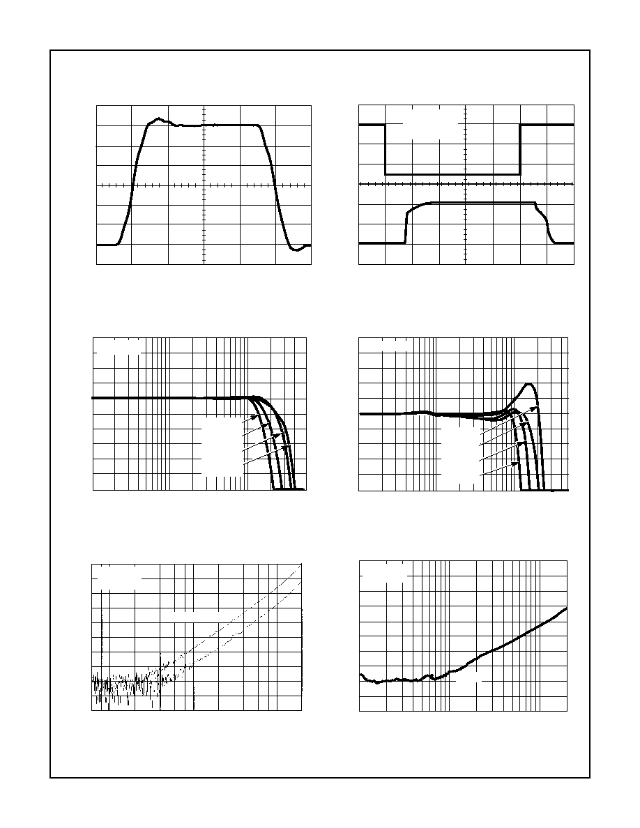
Typical Performance Curves
V
SUPPLY
=
±
5V, T
A
= 25
o
C, R
L
= 10k
, Unless Otherwise Specified
FIGURE 3. LARGE SIGNAL PULSE RESPONSE
FIGURE 4. CHANNEL-TO-CHANNEL SWITCHING RESPONSE
FIGURE 5. FREQUENCY RESPONSE
FIGURE 6. GAIN FLATNESS
FIGURE 7. ALL HOSTILE CROSSTALK REJECTION
FIGURE 8. ALL HOSTILE OFF ISOLATION
1.0
0.75
0.5
0.25
0
-0.25
-0.75
-1.0
OUTPUT V
O
L
T
A
GE (V)
TIME (5ns/DIV.)
-0.5
TIME (200ns/DIV.)
OUTPUT V
O
L
T
A
GE (mV)
0
125
250
A1 (V)
0
0.8
1.6
2.4
IN1 = +250mV
A0 = +3V
IN3 = 0V
3
2
1
0
-1
-2
-3
-4
-5
1
10
100
500
C
L
= 49pF
C
L
= 34pF
C
L
= 19pF
C
L
= 11pF
FREQUENCY (MHz)
GAIN (dB)
V
IN
= 1V
P-P
0.4
0.3
0.2
0.1
0
-0.1
-0.2
-0.3
-0.4
1
10
100
500
V
IN
= 1V
P-P
FREQUENCY (MHz)
GAIN (dB)
C
L
= 19pF
C
L
= 11pF
C
L
= 34pF
C
L
= 49pF
-40
-50
-60
-70
-80
-90
-100
-110
-120
0.6
1
200
100
10
CR
OSST
ALK (dB)
FREQUENCY (MHz)
SOIC
V
IN
= 1V
P-P
R
L
= 10k
PDIP (OBSOLETE)
-40
-50
-60
-70
-80
-90
-100
-110
-120
1
10
100
200
V
IN
= 1V
P-P
R
L
= 10
SOIC
FREQUENCY (MHz)
OFF ISOLA
TION (dB)
HA4404B

11
FIGURE 9. TOTAL HARMONIC DISTORTION vs FREQUENCY
FIGURE 10. INPUT CAPACITANCE vs FREQUENCY
Typical Performance Curves
V
SUPPLY
=
±
5V, T
A
= 25
o
C, R
L
= 10k
, Unless Otherwise Specified (Continued)
T
O
T
AL HARMONIC DIST
OR
TION (%)
0.2
0.15
0.1
0.05
0
10
20
30
50
60
70
80
90
100
40
V
IN
= 1V
P-P
R
L
= 1k
FREQUENCY (MHz)
1
10
100
FREQUENCY (MHz)
1.5
1.8
2.1
2.4
2.7
3.0
3.3
3.6
3.9
4.2
4.5
500
CH. 0
CH. 3
CH. 1
CH. 2
INPUT CAP
A
CIT
ANCE (pF)
HA4404B

12
Die Characteristics
DIE DIMENSIONS:
65 mils x 118 mils x 19 mils
1640
µ
m x 3000
µ
m x 483
µ
m
METALLIZATION:
Type: Metal 1: AlCu (1%)/TiW
Thickness: Metal 1: 6k
≈
±
0.8k
≈
Type: Metal 2: AlCu (1%)
Thickness: Metal 2: 16k
≈
±
1.1k
≈
PASSIVATION:
Type: Nitride
Thickness: 4k
≈
±
0.5k
≈
TRANSISTOR COUNT:
200
SUBSTRATE POTENTIAL (Powered Up):
V-
Metallization Mask Layout
HA4404B
IN0
GND
IN1
IN2
NC
GND
GND
T0
T1
T2
IN3
V-
T3
NC
NC
OUT
CS
A1
A0
V+
HA4404B

13
HA4404B
Small Outline Plastic Packages (SOIC)
NOTES:
1. Symbols are defined in the "MO Series Symbol List" in Section 2.2 of
Publication Number 95.
2. Dimensioning and tolerancing per ANSI Y14.5M-1982.
3. Dimension "D" does not include mold flash, protrusions or gate burrs.
Mold flash, protrusion and gate burrs shall not exceed 0.15mm (0.006
inch) per side.
4. Dimension "E" does not include interlead flash or protrusions. Interlead
flash and protrusions shall not exceed 0.25mm (0.010 inch) per side.
5. The chamfer on the body is optional. If it is not present, a visual index
feature must be located within the crosshatched area.
6. "L" is the length of terminal for soldering to a substrate.
7. "N" is the number of terminal positions.
8. Terminal numbers are shown for reference only.
9. The lead width "B", as measured 0.36mm (0.014 inch) or greater above
the seating plane, shall not exceed a maximum value of 0.61mm
(0.024 inch).
10. Controlling dimension: MILLIMETER. Converted inch dimensions are
not necessarily exact.
INDEX
AREA
E
D
N
1
2
3
-B-
0.25(0.010)
C A
M
B S
e
-A-
L
B
M
-C-
A1
A
SEATING PLANE
0.10(0.004)
h x 45
o
C
H
0.25(0.010)
B
M
M
M16.15
(JEDEC MS-012-AC ISSUE C)
16 LEAD NARROW BODY SMALL OUTLINE PLASTIC
PACKAGE
SYMBOL
INCHES
MILLIMETERS
NOTES
MIN
MAX
MIN
MAX
A
0.0532
0.0688
1.35
1.75
-
A1
0.0040
0.0098
0.10
0.25
-
B
0.013
0.020
0.33
0.51
9
C
0.0075
0.0098
0.19
0.25
-
D
0.3859
0.3937
9.80
10.00
3
E
0.1497
0.1574
3.80
4.00
4
e
0.050 BSC
1.27 BSC
-
H
0.2284
0.2440
5.80
6.20
-
h
0.0099
0.0196
0.25
0.50
5
L
0.016
0.050
0.40
1.27
6
N
16
16
7
0
o
8
o
0
o
8
o
-
Rev. 0 12/93