 | –≠–ª–µ–∫—Ç—Ä–æ–Ω–Ω—ã–π –∫–æ–º–ø–æ–Ω–µ–Ω—Ç: HA4600CB | –°–∫–∞—á–∞—Ç—å:  PDF PDF  ZIP ZIP |
TM
3-1
HA4600
480MHz, SOT-23, Video Buffer with Output
Disable
The HA4600 is a very wide bandwidth, unity gain buffer ideal
for professional video switching, HDTV, computer monitor
routing, and other high performance applications. The circuit
features very low power dissipation (105mW Enabled, 1mW
Disabled), excellent differential gain and phase, and very
high off isolation. When disabled, the output is switched to a
high impedance state, making the HA4600 ideal for routing
matrix equipment and video multiplexers.
The HA4600 also features fast switching and symmetric slew
rates. A typical application for the HA4600 is interfacing
Intersil's wide range of video crosspoint switches.
For applications requiring a tally output (enable indicator),
please refer to the HA4201 data sheet.
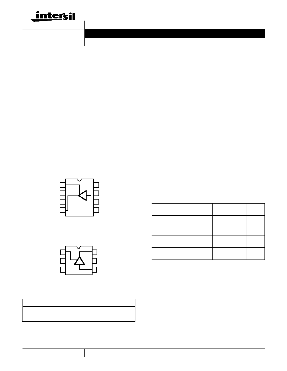
Pinouts
HA4600
(PDIP, SOIC)
TOP VIEW
HA4600
(SOT-23)
TOP VIEW
Features
∑ Micro Package Available. . . . . . . . . . . . . . . . . . . . SOT-23
∑ Low Power Dissipation . . . . . . . . . . . . . . . . . . . . . 105mW
∑ Symmetrical Slew Rates . . . . . . . . . . . . . . . . . . 1700V/
µ
s
∑ 0.1dB Gain Flatness. . . . . . . . . . . . . . . . . . . . . . . 250MHz
∑ Off Isolation (100MHz) . . . . . . . . . . . . . . . . . . . . . . . 85dB
∑ Differential Gain and Phase . . . . . . . 0.01%/0.01 Degrees
∑ High ESD Rating . . . . . . . . . . . . . . . . . . . . . . . . . >1800V
∑ TTL Compatible Enable Input
∑ Improved Replacement for GB4600
Applications
∑ Professional Video Switching and Routing
∑ Video Multiplexers
∑ HDTV
∑ Computer Graphics
∑ RF Switching and Routing
∑ PCM Data Routing
Truth Table
EN
OUT
0
High Z
1
Active
EN
V-
V+
OUT
1
2
3
4
8
7
6
5
GND
IN
NC
NC
V+
V-
OUT
IN
GND
EN
1
2
3
6
5
4
Ordering Information
PART NUMBER
(BRAND)
TEMP.
RANGE (
o
C)
PACKAGE
PKG.
NO.
HA4600CP
0 to 70
8 Ld PDIP
E8.3
HA4600CB
(H4600CB)
0 to 70
8 Ld SOIC
M8.15
HA4600CB96
(H4600CB)
0 to 70
8 Ld SOIC Tape
and Reel
M8.15
HA4600CH96
(4600)
0 to 70
6 Ld SOT-23 Tape
and Reel
P6.064
Data Sheet
June 2000
File Number
3990.6
CAUTION: These devices are sensitive to electrostatic discharge; follow proper IC Handling Procedures.
1-888-INTERSIL or 321-724-7143
|
Intersil and Design is a trademark of Intersil Corporation.
|
Copyright
©
Intersil Corporation 2000

3-2
Absolute Maximum Ratings
Thermal Information
Voltage Between V+ and V- . . . . . . . . . . . . . . . . . . . . . . . . . . . . 12V
Input Voltage . . . . . . . . . . . . . . . . . . . . . . . . . . . . . . . . . . . V
SUPPLY
Digital Input Current (Note 2) . . . . . . . . . . . . . . . . . . . . . . . . .
±
25mA
Output Current . . . . . . . . . . . . . . . . . . . . . . . . . . . . . . . . . . . . . 20mA
ESD Rating
Human Body Model (Per MIL-STD-883 Method 3015.7) . . . . 1800V
Operating Conditions
Temperature Range . . . . . . . . . . . . . . . . . . . . . . . . . . . 0
o
C to 70
o
C
Thermal Resistance (Typical, Note 1)
JA
(
o
C/W)
PDIP Package . . . . . . . . . . . . . . . . . . . . . . . . . . . . .
130
SOIC Package . . . . . . . . . . . . . . . . . . . . . . . . . . . . .
170
SOT-23 Package . . . . . . . . . . . . . . . . . . . . . . . . . . .
210
Maximum Junction Temperature (Die) . . . . . . . . . . . . . . . . . . . 175
o
C
Maximum Junction Temperature (Plastic Package) . . . . . . . 150
o
C
Maximum Storage Temperature Range . . . . . . . . . . -65
o
C to 150
o
C
Maximum Lead Temperature (Soldering 10s) . . . . . . . . . . . . 300
o
C
(SOIC and SOT-23 - Lead Tips Only)
CAUTION: Stresses above those listed in "Absolute Maximum Ratings" may cause permanent damage to the device. This is a stress only rating and operation of the
device at these or any other conditions above those indicated in the operational sections of this specification is not implied.
NOTES:
1.
JA
is measured with the component mounted on an evaluation PC board in free air.
2. If an input signal is applied before the supplies are powered up, the input current must be limited to this maximum value.
Electrical Specifications
V
SUPPLY
=
±
5V, R
L
= 10k
, V
EN
= 2.0V, Unless Otherwise Specified
PARAMETER
TEST CONDITIONS
TEMP. (
o
C)
MIN
TYP
MAX
UNITS
DC SUPPLY CHARACTERISTICS
Supply Voltage
Full
±
4.5
±
5.0
±
5.5
V
Supply Current (V
OUT
= 0V)
V
EN
= 2V
25, 70
-
10.5
13
mA
V
EN
= 2V
0
-
-
14.5
mA
V
EN
= 0.8V
25, 70
-
100
115
µ
A
V
EN
= 0.8V
0
-
100
125
µ
A
ANALOG DC CHARACTERISTICS
Output Voltage Swing without Clipping
V
OUT
= V
IN
±
V
IO
±
20mV
25, 70
±
2.7
±
2.8
-
V
0
±
2.4
±
2.5
-
V
Output Current
Full
15
20
-
mA
Input Bias Current
Full
-
30
50
µ
A
Output Offset Voltage
25
-10
-
10
mV
Output Offset Voltage Drift (Note 3)
Full
-
25
50
µ
V/
o
C
SWITCHING CHARACTERISTICS
Turn-On Time
25
-
160
-
ns
Turn-Off Time
25
-
320
-
ns
DIGITAL DC CHARACTERISTICS
Input Logic High Voltage
Full
2
-
-
V
Input Logic Low Voltage
Full
-
-
0.8
V
EN Input Current
0V to 4V
Full
-2
-
2
µ
A
AC CHARACTERISTICS
Insertion Loss
1V
P-P
Full
-
0.04
0.05
dB
-3dB Bandwidth
R
S
= 82
, C
L
= 10pF
25
-
480
-
MHz
R
S
= 43
, C
L
= 15pF
25
-
380
-
MHz
R
S
= 36
, C
L
= 21pF
25
-
370
-
MHz
HA4600

3-3
AC Test Circuit
NOTE: C
L
= C
X
+ Test Fixture Capacitance.
PC Board Layout
The frequency response of this circuit depends greatly on the
care taken in designing the PC board. The use of low
inductance components such as chip resistors and chip
capacitors is strongly recommended, while a solid ground
plane is a must!
Attention should be given to decoupling the power supplies.
A large value (10
µ
F) tantalum in parallel with a small value
(0.1
µ
F) chip capacitor works well in most cases.
Keep input and output traces as short as possible, because
trace inductance and capacitance can easily become the
performance limiting items.
Application Information
General
The HA4600 is a unity gain buffer that is optimized for high
performance video applications. The output disable function
makes it ideal for the matrix element in small, high input-to-
output isolation switchers and routers. This buffer contains no
feedback or gain setting resistors, so the output is a true high
impedance load when the IC is disabled (EN = 0). The HA4600
also excels as an input buffer for routers with a large number of
outputs (i.e. each input must connect to a large number of
outputs) and delivers performance superior to most video
amplifiers at a fraction of the cost. As an input buffer, the
HA4600's low input capacitance and high input resistance
provide excellent video terminations when used with an
external 75
resistor.
Frequency Response
Most applications utilizing the HA4600 require a series
output resistor, R
S
, to tune the response for the specific load
capacitance, C
L
, driven. Bandwidth and slew rate degrade
as C
L
increases (as shown in the Electrical Specification
table), so give careful consideration to component
placement to minimize trace length. As an example, -3dB
bandwidth decreases to 160MHz for C
L
= 100pF, R
S
= 0
.
In big matrix configurations where C
L
is large, better
±
0.1dB Flat Bandwidth
R
S
= 82
, C
L
= 10pF
25
-
250
-
MHz
R
S
= 43
, C
L
= 15pF
25
-
175
-
MHz
R
S
= 36
, C
L
= 21pF
25
-
170
-
MHz
Input Resistance
Full
200
400
-
k
Input Capacitance
Full
-
1.0
-
pF
Enabled Output Resistance
Full
-
15
-
Disabled Output Capacitance
V
EN
= 0.8V
Full
-
2.0
-
pF
Differential Gain (Note 3)
4.43MHz
25
-
0.01
0.02
%
Differential Phase (Note 3)
4.43MHz
25
-
0.01
0.02
Degrees
Off Isolation
1V
P-P
, 100MHz,
V
EN
= 0.8V, R
L
= 10
Full
-
85
-
dB
Slew Rate (1.5V
P-P
, +SR/-SR)
R
S
= 82
, C
L
= 10pF
25
-
1750/1770
-
V/
µ
s
R
S
= 43
, C
L
= 15pF
25
-
1460/1360
-
V/
µ
s
R
S
= 36
, C
L
= 21pF
25
-
1410/1360
-
V/
µ
s
Total Harmonic Distortion (Note 3)
Full
-
0.01
0.1
%
Disabled Output Resistance
Full
-
12
-
M
NOTE:
3. This parameter is not tested. The limits are guaranteed based on lab characterization, and reflect lot-to-lot variation.
Electrical Specifications
V
SUPPLY
=
±
5V, R
L
= 10k
, V
EN
= 2.0V, Unless Otherwise Specified (Continued)
PARAMETER
TEST CONDITIONS
TEMP. (
o
C)
MIN
TYP
MAX
UNITS
500
400
510
75
V
OUT
V
IN
75
R
S
HA4600
HFA1100
+
-
C
X
10k
HA4600

3-4
frequency response is obtained by cascading two levels of
crosspoints in the case of multiplexed outputs (see Figure 2),
or distributing the load between two drivers if C
L
is due to
bussing and subsequent stage input capacitance.
Control Signals
EN - The ENABLE input is a TTL/CMOS compatible, active
high input. When driven low this input forces the output to a
true high impedance state and reduces the power
dissipation by two orders of magnitude. The EN input has no
on-chip pull-up resistor, so it must be connected to a logic
high (recommend V+) if the enable function isn't utilized.
Switcher/Router Applications
Figure 1 illustrates one possible implementation of a
wideband, low power, 4 x 4 switcher/router. A 4 x 4
switcher/router allows any of the four outputs to be driven by
any one of the four inputs (e.g. each of the four inputs may
connect to a different output, or an input may connect to
multiple outputs). This application utilizes the HA4600 for the
input buffer, the HA4404 (4 x 1 crosspoint switch) as the
switch matrix, and the HFA1112 (programmable gain buffer)
as the gain of two output driver. Figure 2 details a 16 x 1
switcher (basically a 16:1 MUX) which uses the HA4600 in a
cascaded stage configuration to minimize capacitive loading
at each output node, thus increasing system bandwidth.
Power Up Considerations
No signals should be applied to the analog or digital inputs
before the power supplies are activated. Latch-up may occur
if the inputs are driven at the time of power up. To prevent
latch-up, the input currents during power up must not exceed
the values listed in the Absolute Maximum Ratings.
Intersil's Crosspoint Family
Intersil offers a variety of 1 x 1 and 4 x 1 crosspoint switches. In
addition to the HA4600, the 1 x 1 family includes the HA4201
which is an essentially similar device that includes a Tally output
(enable indicator). The 4 x 1 family is comprised of the HA4314,
HA4404, and HA4344. The HA4314 is a 14 lead basic 4 x 1
crosspoint. The HA4404 is a 16 lead device with Tally outputs
to indicate the selected channel. The HA4344 is a 16 lead
crosspoint with synchronized control lines (A0, A1, CS). With
synchronization, the control information for the next channel
switch can be loaded into the crosspoint without affecting the
current state. On a subsequent clock edge the stored control
state effects the desired channel switch.
-
INPUT BUFFERS
SWITCH MATRIX
OUTPUT BUFFERS
(HFA1112 OR HFA1115)
OUT
SOURCE3
IN0
T0
HA4404
CS
T3
IN3
EN
OUT0
10k
75
R
S
HA4600
OUT
IN0
T0
HA4404
CS
T3
IN3
OUT
IN0
T0
HA4404
CS
T3
IN3
OUT
IN0
T0
HA4404
CS
T3
IN3
75
OUT1
75
R
S
R
S
R
S
R
S
X2
+
OUT
SOURCE0
EN
75
R
S
HA4600
OUT
SOURCE1
75
SOURCE2
75
OUT2
75
OUT3
75
10k
X2
X2
X2
-
+
-
+
-
+
FIGURE 1. 4 x 4 SWITCHER/ROUTER APPLICATION
HA4600

3-5
SOURCE0
75
HA4600
OUT
IN0
T0
T3
IN3
SOURCE3
75
SOURCE4
75
OUT
IN3
T0
T3
IN0
SOURCE7
75
R
S
SOURCE8
75
R
S
HA4600
OUT
IN0
T0
T3
IN3
SOURCE11
75
SOURCE12
75
R
S
OUT
IN3
T0
T3
IN0
SOURCE15
75
R
S
HA4404
75
+
-
X2
OUT
10k
10k
HA4404
R
S
R
S
SWITCHING MATRIX
OUTPUT BUFFER
ISOLATION MUX
HFA1112 OR HFA1115
IN2
IN1
IN2
IN1
IN2
IN1
IN2
IN1
EN
EN
FIGURE 2. 16 x 1 SWITCHER APPLICATION
HA4600
3-6
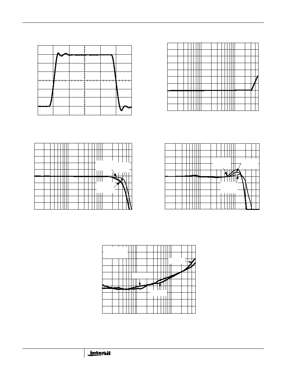
Typical Performance Curves
V
SUPPLY
=
±
5V, T
A
= 25
o
C, R
L
= 10k
, Unless Otherwise Specified
FIGURE 3. LARGE SIGNAL PULSE RESPONSE
FIGURE 4. INPUT CAPACITANCE vs FREQUENCY
FIGURE 5. FREQUENCY RESPONSE
FIGURE 6. GAIN FLATNESS
FIGURE 7. OFF ISOLATION
1.0
0.75
0.5
0.25
0
-0.25
-0.5
-0.75
-1.0
OUTPUT V
O
L
T
A
GE (V)
TIME (5ns/DIV.)
1
10
100
FREQUENCY (MHz)
0.75
0.80
0.85
0.90
0.95
1.0
1.05
1.10
1.15
1.20
1.25
500
INPUT CAP
A
CIT
ANCE (pF)
12
9
6
3
0
-3
-6
-9
-12
1
10
100
750
GAIN (dB)
FREQUENCY (MHz)
R
S
= 36
C
L
= 21pF
R
S
= 82
C
L
= 10pF
R
S
= 43
C
L
= 15pF
0.4
0.3
0.2
0.1
0
-0.1
-0.2
-0.3
-0.4
1
10
100
500
GAIN (dB)
FREQUENCY (MHz)
R
S
= 36
C
L
= 21pF
R
S
= 82
C
L
= 10pF
R
S
= 43
C
L
= 15pF
-50
-60
-70
-80
-90
-100
-110
-120
-130
1
10
100
500
OFF ISOLA
TION (dB)
FREQUENCY (MHz)
V
IN
= 1V
P-P
R
L
= 10
PDIP, SOIC
PDIP, SOIC
SOT-23
HA4600
7
All Intersil semiconductor products are manufactured, assembled and tested under ISO9000 quality systems certification.
Intersil semiconductor products are sold by description only. Intersil Corporation reserves the right to make changes in circuit design and/or specifications at any time with-
out notice. Accordingly, the reader is cautioned to verify that data sheets are current before placing orders. Information furnished by Intersil is believed to be accurate and
reliable. However, no responsibility is assumed by Intersil or its subsidiaries for its use; nor for any infringements of patents or other rights of third parties which may result
from its use. No license is granted by implication or otherwise under any patent or patent rights of Intersil or its subsidiaries.
For information regarding Intersil Corporation and its products, see web site www.intersil.com
Sales Office Headquarters
NORTH AMERICA
Intersil Corporation
P. O. Box 883, Mail Stop 53-204
Melbourne, FL 32902
TEL: (321) 724-7000
FAX: (321) 724-7240
EUROPE
Intersil SA
Mercure Center
100, Rue de la Fusee
1130 Brussels, Belgium
TEL: (32) 2.724.2111
FAX: (32) 2.724.22.05
ASIA
Intersil Ltd.
8F-2, 96, Sec. 1, Chien-kuo North,
Taipei, Taiwan 104
Republic of China
TEL: 886-2-2515-8508
FAX: 886-2-2515-8369
Die Characteristics
DIE DIMENSIONS:
51 mils x 36 mils x 19 mils
1290
µ
m x 910
µ
m x 483
µ
m
METALLIZATION:
Type: Metal 1: AICu (1%)/TiW
Thickness: Metal 1: 6k≈
±
0.8k≈
Type: Metal 2: AICu (1%)
Thickness: Metal 2: 16k≈
±
1.1k≈
SUBSTRATE POTENTIAL (Powered Up):
V-
PASSIVATION:
Type: Nitride
Thickness: 4k≈
±
0.5k≈
TRANSISTOR COUNT:
53
Metallization Mask Layout
HA4600
EN
V-
V+
OUT
NC
IN
GND
HA4600