 | –≠–ª–µ–∫—Ç—Ä–æ–Ω–Ω—ã–π –∫–æ–º–ø–æ–Ω–µ–Ω—Ç: HA5023IP | –°–∫–∞—á–∞—Ç—å:  PDF PDF  ZIP ZIP |

1
CAUTION: These devices are sensitive to electrostatic discharge; follow proper IC Handling Procedures.
http://www.intersil.com or 407-727-9207 | Copyright © Intersil Corporation 1999
HA5023
Dual 125MHz Video Current
Feedback Amplifier
The HA5023 is a wide bandwidth high slew rate dual
amplifier optimized for video applications and gains between
1 and 10. It is a current feedback amplifier and thus yields
less bandwidth degradation at high closed loop gains than
voltage feedback amplifiers.
The low differential gain and phase, 0.1dB gain flatness, and
ability to drive two back terminated 75
cables, make this
amplifier ideal for demanding video applications.
The current feedback design allows the user to take
advantage of the amplifier's bandwidth dependency on the
feedback resistor. By reducing R
F
, the bandwidth can be
increased to compensate for decreases at higher closed
loop gains or heavy output loads.
The performance of the HA5023 is very similar to the
popular Intersil HA-5020
.
Features
∑ Wide Unity Gain Bandwidth . . . . . . . . . . . . . . . . . 125MHz
∑ Slew Rate . . . . . . . . . . . . . . . . . . . . . . . . . . . . . . . 475V/
µ
s
∑ Input Offset Voltage . . . . . . . . . . . . . . . . . . . . . . . . 800
µ
V
∑ Differential Gain . . . . . . . . . . . . . . . . . . . . . . . . . . . 0.03%
∑ Differential Phase . . . . . . . . . . . . . . . . . . . . 0.03 Degrees
∑ Supply Current (per Amplifier) . . . . . . . . . . . . . . . . 7.5mA
∑ ESD Protection. . . . . . . . . . . . . . . . . . . . . . . . . . . . 4000V
∑ Guaranteed Specifications at
±
5V Supplies
Applications
∑ Video Gain Block
∑ Video Distribution Amplifier/RGB Amplifier
∑ Flash A/D Driver
∑ Current to Voltage Converter
∑ Medical Imaging
∑ Radar and Imaging Systems
∑ Video Switching and Routing
Pinout
HA5023
(PDIP, SOIC)
TOP VIEW
Ordering Information
PART NUMBER
(BRAND)
TEMP.
RANGE (
o
C)
PACKAGE
PKG.
NO.
HA5023IP
-40 to 85
8 Ld PDIP
E8.3
HA5023IB
(H5023I)
-40 to 85
8 Ld SOIC
M8.15
HA5023EVAL
High Speed Op Amp DIP Evaluation Board
OUT1
-IN1
+IN1
V-
1
2
3
4
8
7
6
5
V+
OUT2
-IN2
+IN2
+
-
+
-
September 1998
File Number
3393.6
2
Absolute Maximum Ratings
Thermal Information
Voltage Between V+ and V- Terminals. . . . . . . . . . . . . . . . . . . . .36V
DC Input Voltage (Note 3) . . . . . . . . . . . . . . . . . . . . . . . .
±
V
SUPPLY
Differential Input Voltage . . . . . . . . . . . . . . . . . . . . . . . . . . . . . . .10V
Output Current (Note 4) . . . . . . . . . . . . . . . . .Short Circuit Protected
ESD Rating (Note 3)
Human Body Model (Per MIL-STD-883 Method 3015.7) . . . 2000V
Operating Conditions
Temperature Range . . . . . . . . . . . . . . . . . . . . . . . . . . -40
o
C to 85
o
C
Supply Voltage Range (Typical) . . . . . . . . . . . . . . . . .
±
4.5V to
±
15V
Thermal Resistance (Typical, Note 2)
JA
(
o
C/W)
PDIP Package . . . . . . . . . . . . . . . . . . . . . . . . . . . . .
130
SOIC Package . . . . . . . . . . . . . . . . . . . . . . . . . . . . .
160
Maximum Junction Temperature (Note 1) . . . . . . . . . . . . . . . . .175
o
C
Maximum Junction Temperature (Plastic Package, Note 1) . .150
o
C
Maximum Storage Temperature Range . . . . . . . . . . -65
o
C to 150
o
C
Maximum Lead Temperature (Soldering 10s) . . . . . . . . . . . . 300
o
C
(SOIC - Lead Tips Only)
CAUTION: Stresses above those listed in "Absolute Maximum Ratings" may cause permanent damage to the device. This is a stress only rating and operation of the
device at these or any other conditions above those indicated in the operational sections of this specification is not implied.
NOTES:
1. Maximum power dissipation, including output load, must be designed to maintain junction temperature below 175
o
C for die, and below 150
o
C
for plastic packages. See Application Information section for safe operating area information.
2.
JA
is measured with the component mounted on an evaluation PC board in free air.
3. The non-inverting input of unused amplifiers must be connected to GND.
4. Output is protected for short circuits to ground. Brief short circuits to ground will not degrade reliability, however, continuous (100% duty cycle)
output current should not exceed 15mA for maximum reliability.
Electrical Specifications
V
SUPPLY
=
±
5V, R
F
= 1k
,
A
V
= +1, R
L
= 400
,
C
L
10pF,
Unless Otherwise Specified
PARAMETER
TEST CONDITIONS
(NOTE 9)
TEST
LEVEL
TEMP.
(
o
C)
MIN
TYP
MAX
UNITS
INPUT CHARACTERISTICS
Input Offset Voltage (V
IO
)
A
25
-
0.8
3
mV
A
Full
-
-
5
mV
Delta V
IO
Between Channels
A
Full
-
1.2
3.5
mV
Average Input Offset Voltage Drift
B
Full
-
5
-
µ
V/
o
C
V
IO
Common Mode Rejection Ratio
Note 5
A
25
53
-
-
dB
A
Full
50
-
-
dB
V
IO
Power Supply Rejection Ratio
±
3.5V
V
S
±
6.5V
A
25
60
-
-
dB
A
Full
55
-
-
dB
Input Common Mode Range
Note 5
A
Full
±
2.5
-
-
V
Non-Inverting Input (+IN) Current
A
25
-
3
8
µ
A
A
Full
-
-
20
µ
A
+IN Common Mode Rejection
(+I
BCMR
=
)
Note 5
A
25
-
-
0.15
µ
A/V
A
Full
-
-
0.5
µ
A/V
+IN Power Supply Rejection
±
3.5V
V
S
±
6.5V
A
25
-
-
0.1
µ
A/V
A
Full
-
-
0.3
µ
A/V
Inverting Input (-IN) Current
A
25, 85
-
4
12
µ
A
A
-40
-
10
30
µ
A
Delta -IN BIAS Current Between Channels
A
25, 85
-
6
15
µ
A
A
-40
-
10
30
µ
A
1
+R
IN
HA5023
3
-IN Common Mode Rejection
Note 5
A
25
-
-
0.4
µ
A/V
A
Full
-
-
1.0
µ
A/V
-IN Power Supply Rejection
±
3.5V
V
S
±
6.5V
A
25
-
-
0.2
µ
A/V
A
Full
-
-
0.5
µ
A/V
Input Noise Voltage
f = 1kHz
B
25
-
4.5
-
nV/
Hz
+Input Noise Current
f = 1kHz
B
25
-
2.5
-
pA/
Hz
-Input Noise Current
f = 1kHz
B
25
-
25.0
-
pA/
Hz
TRANSFER CHARACTERISTICS
Transimpedence
Note 11
A
25
1.0
-
-
M
A
Full
0.85
-
-
M
Open Loop DC Voltage Gain
R
L
= 400
, V
OUT
=
±
2.5V
A
25
70
-
-
dB
A
Full
65
-
-
dB
Open Loop DC Voltage Gain
R
L
= 100
, V
OUT
=
±
2.5V
A
25
50
-
-
dB
A
Full
45
-
-
dB
OUTPUT CHARACTERISTICS
Output Voltage Swing
R
L
= 150
A
25
±
2.5
±
3.0
-
V
A
Full
±
2.5
±
3.0
-
V
Output Current
R
L
= 150
B
Full
±
16.6
±
20.0
-
mA
Output Current, Short Circuit
V
IN
=
±
2.5V, V
OUT
= 0V
A
Full
±
40
±
60
-
mA
POWER SUPPLY CHARACTERISTICS
Supply Voltage Range
A
25
5
-
15
V
Quiescent Supply Current
A
Full
-
7.5
10
mA/Op Amp
AC CHARACTERISTICS (A
V
= +1)
Slew Rate
Note 6
B
25
275
350
-
V/
µ
s
Full Power Bandwidth
Note 7
B
25
22
28
-
MHz
Rise Time
Note 8
B
25
-
6
-
ns
Fall Time
Note 8
B
25
-
6
-
ns
Propagation Delay
Note 8
B
25
-
6
-
ns
Overshoot
B
25
-
4.5
-
%
-3dB Bandwidth
V
OUT
= 100mV
B
25
-
125
-
MHz
Settling Time to 1%
2V Output Step
B
25
-
50
-
ns
Settling Time to 0.25%
2V Output Step
B
25
-
75
-
ns
Electrical Specifications
V
SUPPLY
=
±
5V, R
F
= 1k
,
A
V
= +1, R
L
= 400
,
C
L
10pF,
Unless Otherwise Specified (Continued)
PARAMETER
TEST CONDITIONS
(NOTE 9)
TEST
LEVEL
TEMP.
(
o
C)
MIN
TYP
MAX
UNITS
HA5023
4
AC CHARACTERISTICS (A
V
= +2, R
F
= 681
)
Slew Rate
Note 6
B
25
-
475
-
V/
µ
s
Full Power Bandwidth
Note 7
B
25
-
26
-
MHz
Rise Time
Note 8
B
25
-
6
-
ns
Fall Time
Note 8
B
25
-
6
-
ns
Propagation Delay
Note 8
B
25
-
6
-
ns
Overshoot
B
25
-
12
-
%
-3dB Bandwidth
V
OUT
= 100mV
B
25
-
95
-
MHz
Settling Time to 1%
2V Output Step
B
25
-
50
-
ns
Settling Time to 0.25%
2V Output Step
B
25
-
100
-
ns
Gain Flatness
5MHz
B
25
-
0.02
-
dB
20MHz
B
25
-
0.07
-
dB
AC CHARACTERISTICS (A
V
= +10, R
F
= 383
)
Slew Rate
Note 6
B
25
350
475
-
V/
µ
s
Full Power Bandwidth
Note 7
B
25
28
38
-
MHz
Rise Time
Note 8
B
25
-
8
-
ns
Fall Time
Note 8
B
25
-
9
-
ns
Propagation Delay
Note 8
B
25
-
9
-
ns
Overshoot
B
25
-
1.8
-
%
-3dB Bandwidth
V
OUT
= 100mV
B
25
-
65
-
MHz
Settling Time to 1%
2V Output Step
B
25
-
75
-
ns
Settling Time to 0.1%
2V Output Step
B
25
-
130
-
ns
VIDEO CHARACTERISTICS
Differential Gain (Note 10)
R
L
= 150
B
25
-
0.03
-
%
Differential Phase (Note 10)
R
L
= 150
B
25
-
0.03
-
Degrees
NOTES:
5. V
CM
=
±
2.5V. At -40
o
C Product is tested at V
CM
=
±
2.25V because Short Test Duration does not allow self heating.
6. V
OUT
switches from -2V to +2V, or from +2V to -2V. Specification is from the 25% to 75% points.
7.
.
8. R
L
= 100
, V
OUT
= 1V. Measured from 10% to 90% points for rise/fall times; from 50% points of input and output for propagation delay.
9. A. Production Tested; B. Typical or Guaranteed Limit based on characterization; C. Design Typical for information only.
10. Measured with a VM700A video tester using an NTC-7 composite VITS.
11. V
OUT
=
±
2.5V. At -40
o
C Product is tested at V
OUT
=
±
2.25V because Short Test Duration does not allow self heating.
Electrical Specifications
V
SUPPLY
=
±
5V, R
F
= 1k
,
A
V
= +1, R
L
= 400
,
C
L
10pF,
Unless Otherwise Specified (Continued)
PARAMETER
TEST CONDITIONS
(NOTE 9)
TEST
LEVEL
TEMP.
(
o
C)
MIN
TYP
MAX
UNITS
FPBW
Slew Rate
2
V
PEAK
-----------------------------
; V
PEAK
2V
=
=
HA5023
5
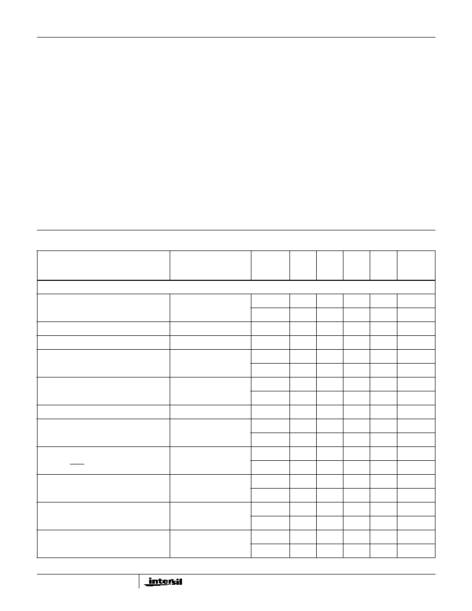
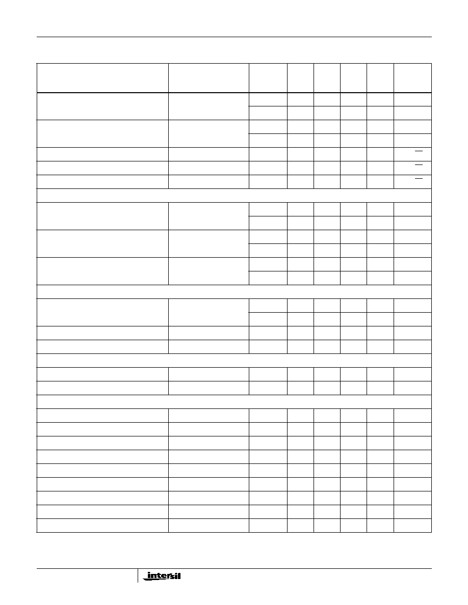
Test Circuits and Waveforms
FIGURE 1. TEST CIRCUIT FOR TRANSIMPEDANCE MEASUREMENTS
FIGURE 2. SMALL SIGNAL PULSE RESPONSE CIRCUIT
FIGURE 3. LARGE SIGNAL PULSE RESPONSE CIRCUIT
NOTE:
12. A series input resistor of
100
is recommended to limit input currents in case input signals are present before the HA5023 is powered up.
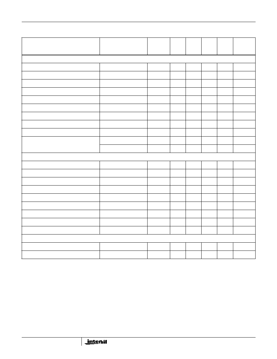
FIGURE 4. SMALL SIGNAL RESPONSE
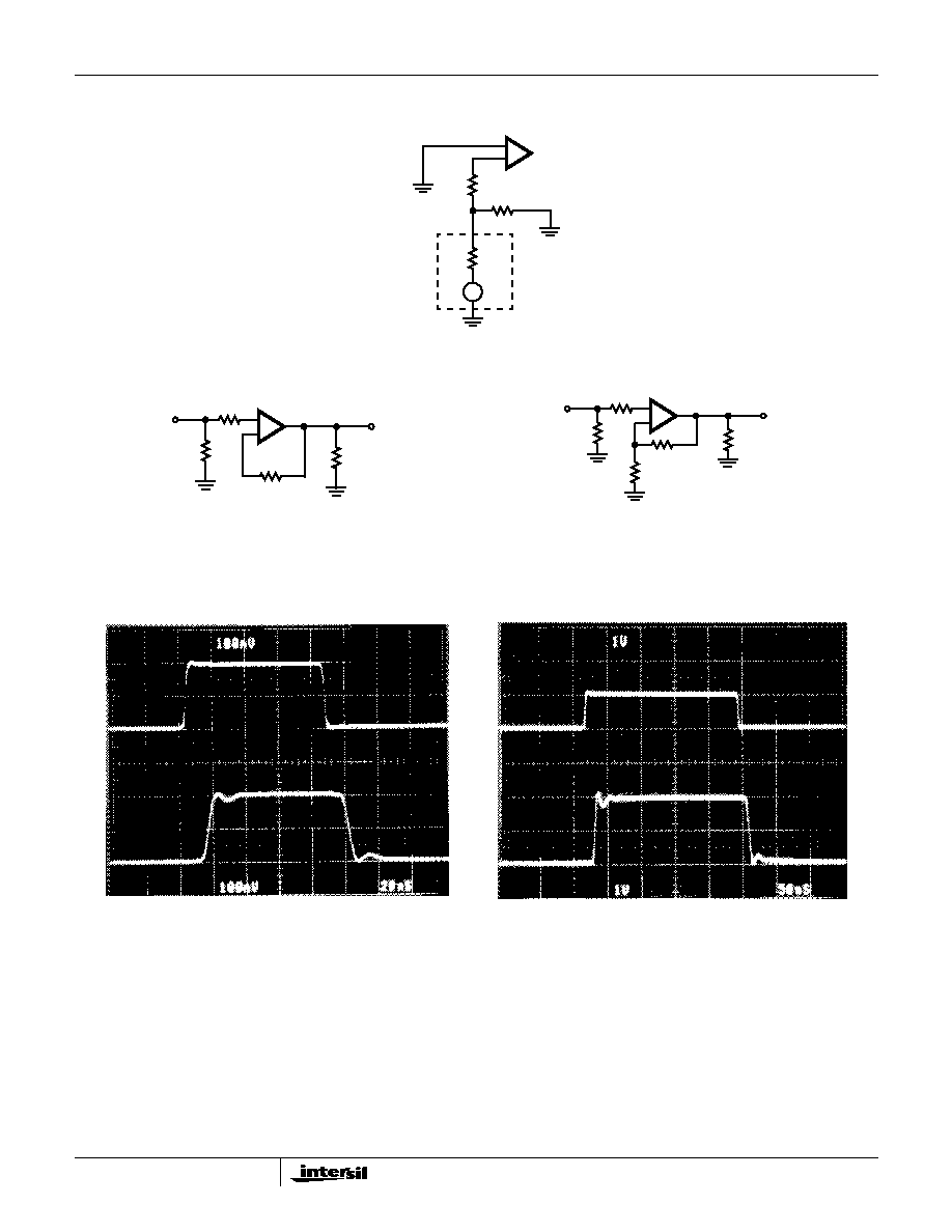
FIGURE 5. LARGE SIGNAL RESPONSE
+
-
50
50
DUT
HP4195
NETWORK
ANALYZER
V
IN
V
OUT
R
L
R
F
, 1k
100
50
+
-
DUT
100
(NOTE 12)
V
IN
V
OUT
R
L
R
F
, 681
400
50
+
-
DUT
R
I
681
100
(NOTE 12)
Vertical Scale: V
IN
= 100mV/Div., V
OUT
= 100mV/Div.
Horizontal Scale: 20ns/Div.
Vertical Scale: V
IN
= 1V/Div., V
OUT
= 1V/Div.
Horizontal Scale: 50ns/Div.
HA5023