3-114
CAUTION: These devices are sensitive to electrostatic discharge; follow proper IC Handling Procedures.
http://www.intersil.com or 407-727-9207
|
Copyright
©
Intersil Corporation 1999
HA-5104/883
Low Noise, High Performance,
Quad Operational Amplifier
Description
Low noise and high performance are key words describing
the unity gain stable HA-5104/883. This general purpose
quad amplifier offers an array of dynamic specifications
including 1V/
µ
s slew rate (min), and 8MHz bandwidth (typ).
Complementing these outstanding parameters are very low
noise specifications of 4.3nV/
Hz at 1kHz (typ) or 6nV/
Hz
(max).
Fabricated using the Intersil standard high frequency D.I.
process, these operational amplifiers also offer excellent
input specifications such as 2.5mV (max) offset voltage and
75nA (max) offset current. Complementing these specifica-
tions are 100dB (min) open loop gain and 55dB channel
separation (min). Economically, the HA-5104/883 also con-
sumes a very moderate amount of power (225mW per pack-
age) while also saving board space and cost.
This impressive combination of features make this amplifier
ideally suited for designs ranging from audio amplifiers and
active filters to the most demanding signal conditioning and
instrumentation circuits.
Ordering Information
PART
NUMBER
TEMPERATURE
RANGE
PACKAGE
HA1-5104/883
-55
o
C to +125
o
C
14 Lead CerDIP
HA4-5104/883
-55
o
C to +125
o
C
20 Lead Ceramic LCC
Features
∑ This Circuit is Processed in Accordance to MIL-STD-
883 and is Fully Conformant Under the Provisions of
Paragraph 1.2.1.
∑ Low Input Noise Voltage Density at 1kHz. . 6nV/
Hz (Max)
4.3nV/
Hz (Typ)
∑ Slew Rate . . . . . . . . . . . . . . . . . . . . . . . . . . . 1V/
µ
s (Min)
3V/
µ
s (Typ)
∑ Unity Gain Bandwidth . . . . . . . . . . . . . . . . . 8MHz (Typ)
∑ High Open Loop Gain (Full Temp) . . . . . 100kV/V (Min)
250kV/V (Typ)
∑ High CMRR, PSRR (Full Temp) . . . . . . . . . . . 86dB (Min)
100dB (Typ)
∑ Low Offset Voltage Drift . . . . . . . . . . . . . . 3
µ
V/
o
C (Typ)
∑ No Crossover Distortion
∑ Standard Quad Pinout
Applications
∑ High Q Active Filters
∑ Audio Amplifiers
∑ Integrators
∑ Signal Generators
∑ Instrumentation Amplifiers
July 1994
Spec Number
511014-883
File Number
3710
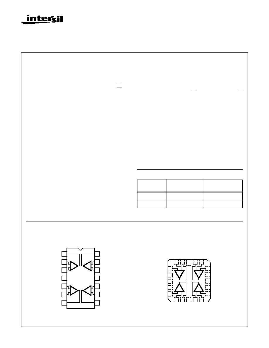
Pinouts
HA-5104/883
(CERDIP)
TOP VIEW
HA-5104/883
(CLCC)
TOP VIEW
1
2
3
4
5
6
7
14
13
12
11
10
9
8
1
+
4
+
2
+
3
+
V+
OUT 1
-IN1
+IN1
+IN2
-IN2
OUT 2
V-
OUT 3
OUT 4
-IN3
+IN3
+IN4
-IN4
-
-
-
-
4
5
6
7
8
9
10
11
12
13
3
2
1
20 19
15
14
18
17
16
4
+
3
+
2
+
1
+
-IN1
OUT 1
NC
OUT 4
-IN4
+IN4
NC
V-
NC
+IN3
+IN1
NC
V+
NC
+IN2
-IN2
OUT 2
NC
OUT 3
-IN3
-
-
-
-

3-115
Specifications HA5104/883
Absolute Maximum Ratings
Thermal Information
Voltage Between V+ and V- Terminals . . . . . . . . . . . . . . . . . . . . 40V
Differential Input Voltage . . . . . . . . . . . . . . . . . . . . . . . . . . . . . . . 7V
Voltage at Either Input Terminal . . . . . . . . . . . . . . . . . . . . . . V+ to V-
Peak Output Current . . . . . . . . . . . . . . . . . . . . . . . . . . . . . Indefinite
(One Amplifier Shorted to Ground)
Junction Temperature (T
J
) . . . . . . . . . . . . . . . . . . . . . . . . . . +175
o
C
Storage Temperature Range . . . . . . . . . . . . . . . . . -65
o
C to +150
o
C
ESD Rating. . . . . . . . . . . . . . . . . . . . . . . . . . . . . . . . . . . . . . <2000V
Lead Temperature (Soldering 10s) . . . . . . . . . . . . . . . . . . . . +300
o
C
Thermal Resistance
JA
JC
CerDIP Package . . . . . . . . . . . . . . . . . . .
75
o
C/W
20
o
C/W
Ceramic LCC Package . . . . . . . . . . . . . .
65
o
C/W
15
o
C/W
Package Power Dissipation Limit at +75
o
C for T
J
+175
o
C
CerDIP Package . . . . . . . . . . . . . . . . . . . . . . . . . . . . . . . . . 1.33W
Ceramic LCC Package . . . . . . . . . . . . . . . . . . . . . . . . . . . . 1.54W
Package Power Dissipation Derating Factor Above +75
o
C
CerDIP Package . . . . . . . . . . . . . . . . . . . . . . . . . . . . . 13.3mW/
o
C
Ceramic LCC Package . . . . . . . . . . . . . . . . . . . . . . . . 15.4mW/
o
C
CAUTION: Stresses above those listed in "Absolute Maximum Ratings" may cause permanent damage to the device. This is a stress only rating and operation
of the device at these or any other conditions above those indicated in the operational sections of this specification is not implied.
Operating Conditions
Operating Temperature Range . . . . . . . . . . . . . . . . -55
o
C to +125
o
C
Operating Supply Voltage
. . . . . . . . . . . . . . . . . . . . . . . . . . ±
5V to
±
15V
V
INCM
1/2 (V+ - V-)
R
L
2k
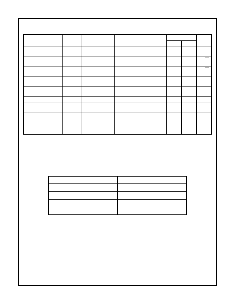
TABLE 1. DC ELECTRICAL PERFORMANCE CHARACTERISTICS
Device Tested at: V
SUPPLY
=
±
15V, R
SOURCE
= 100
, R
LOAD
= 500k
, V
OUT
= 0V, Unless Otherwise Specified.
PARAMETERS
SYMBOL
CONDITIONS
GROUP A
SUBGROUPS
TEMPERATURE
LIMITS
UNITS
MIN
MAX
Input Offset Voltage
V
IO
V
CM
= 0V
1
+25
o
C
-2.5
2.5
mV
2, 3
+125
o
C, -55
o
C
-3.0
3.0
mV
Input Bias Current
+I
B
V
CM
= 0V,
+R
S
= 10k
,
-R
S
= 100
1
+25
o
C
-200
200
nA
2, 3
+125
o
C, -55
o
C
-325
325
nA
-I
B
V
CM
= 0V,
+R
S
= 100
,
-R
S
= 10k
1
+25
o
C
-200
200
nA
2, 3
+125
o
C, -55
o
C
-325
325
nA
Input Offset Current
I
IO
V
CM
= 0V,
+R
S
= 10k
,
-R
S
= 10k
1
+25
o
C
-75
75
nA
2, 3
+125
o
C, -55
o
C
-125
125
nA
Common Mode Range
+CMR
V+ = +3V, V- = -27V
1
+25
o
C
+12
-
V
2, 3
+125
o
C, -55
o
C
+12
-
V
-CMR
V+ = +27V, V- = -3V
1
+25
o
C
-
-12
V
2, 3
+125
o
C, -55
o
C
-
-12
V
Large Signal Voltage
Gain
+A
VOL
V
OUT
= 0V and +10V,
R
L
= 2k
4
+25
o
C
100
-
kV/V
5, 6
+125
o
C, -55
o
C
100
-
kV/V
-A
VOL
V
OUT
= 0V and -10V,
R
L
= 2k
4
+25
o
C
100
-
kV/V
5, 6
+125
o
C, -55
o
C
100
-
kV/V
Common Mode
Rejection Ratio
+CMRR
V
CM
= +5V,
V+ = +10V, V- = -20V,
V
OUT
= -5V
1
+25
o
C
86
-
dB
2, 3
+125
o
C, -55
o
C
86
-
dB
-CMRR
V
CM
= -5V,
V+ = +20V, V- = -10V,
V
OUT
= +5V
1
+25
o
C
86
-
dB
2, 3
+125
o
C, -55
o
C
86
-
dB
Spec Number
511014-883

3-116
Spec Number
511014-883
Specifications HA5104/883
Output Voltage Swing
+V
OUT1
R
L
= 2k
1
+25
o
C
10
-
V
2, 3
+125
o
C, -55
o
C
10
-
V
-V
OUT1
R
L
= 2k
1
+25
o
C
-
-10
V
2, 3
+125
o
C, -55
o
C
-
-10
V
+V
OUT2
R
L
= 10k
1
+25
o
C
12
-
V
2, 3
+125
o
C, -55
o
C
12
-
V
-V
OUT2
R
L
= 10k
1
+25
o
C
-
-12
V
2, 3
+125
o
C, -55
o
C
-
-12
V
Output Current
+I
OUT
V
OUT
= -5V
1
+25
o
C
10
-
mA
2, 3
+125
o
C, -55
o
C
10
-
mA
-I
OUT
V
OUT
= +5V
1
+25
o
C
-
-10
mA
2, 3
+125
o
C, -55
o
C
-
-10
mA
Quiescent Power Supply
Current
+I
CC
V
OUT
= 0V, I
OUT
= 0mA
1
+25
o
C
-
6.5
mA
2, 3
+125
o
C, -55
o
C
-
7.5
mA
-I
CC
V
OUT
= 0V, I
OUT
= 0mA
1
+25
o
C
-6.5
-
mA
2, 3
+125
o
C, -55
o
C
-7.5
-
mA
Power Supply
Rejection Ratio
+PSRR
V
SUP
= 10V,
V+ = +10V, V- = -15V
V+ = +20V, V- = -15V
1
+25
o
C
86
-
dB
2, 3
+125
o
C, -55
o
C
86
-
dB
-PSRR
V
SUP
= 10V,
V+ = +15V, V- = -10V
V+ = +15V, V- = -20V
1
+25
o
C
86
-
dB
2, 3
+125
o
C, -55
o
C
86
-
dB
TABLE 2. AC ELECTRICAL PERFORMANCE CHARACTERISTICS
Device Tested at: V
SUPPLY
=
±
15V, R
SOURCE
= 50
, R
LOAD
= 2k
, C
LOAD
= 50pF, A
VCL
= +1V/V, Unless Otherwise Specified.
PARAMETERS
SYMBOL
CONDITIONS
GROUP A
SUBGROUPS
TEMPERATURE
LIMITS
UNITS
MIN
MAX
Slew Rate
+SR
V
OUT
= -3V to +3V
4
+25
o
C
1
-
V/
µ
s
-SR
V
OUT
= +3V to -3V
4
+25
o
C
1
-
V/
µ
s
Rise and Fall Time
T
R
V
OUT
= 0 to +200mV
10%
T
R
90%
4
+25
o
C
-
200
ns
T
F
V
OUT
= 0 to -200mV
10%
T
F
90%
4
+25
o
C
-
200
ns
Overshoot
+OS
V
OUT
= 0 to +200mV
4
+25
o
C
-
35
%
-OS
V
OUT
= 0 to -200mV
4
+25
o
C
-
35
%
TABLE 1. DC ELECTRICAL PERFORMANCE CHARACTERISTICS (Continued)
Device Tested at: V
SUPPLY
=
±
15V, R
SOURCE
= 100
, R
LOAD
= 500k
, V
OUT
= 0V, Unless Otherwise Specified.
PARAMETERS
SYMBOL
CONDITIONS
GROUP A
SUBGROUPS
TEMPERATURE
LIMITS
UNITS
MIN
MAX
3-117
Spec Number
511014-883
Specifications HA5104/883
TABLE 3. ELECTRICAL PERFORMANCE CHARACTERISTICS
Device Characterized at: V
SUPPLY
=
±
15V, R
LOAD
= 2k
, C
LOAD
= 50pF, A
VCL
= 1V/V, Unless Otherwise Specified.
PARAMETERS
SYMBOL
CONDITIONS
NOTES
TEMPERATURE
LIMITS
UNITS
MIN
MAX
Differential Input
Resistance
R
IN
V
CM
= 0V
1
+25
o
C
250
-
k
Input Noise Voltage
Density
E
N
R
S
= 20
,
f
O
= 1000Hz
1
+25
o
C
-
6
nV
/
Hz
Input Noise Current
Density
I
N
R
S
= 2M
,
f
O
= 1000Hz
1
+25
o
C
-
3
pA
/
Hz
Full Power
Bandwidth
FPBW
V
PEAK
= 10V
1, 2
+25
o
C
32
-
kHz
Minimum Closed Loop
Stable Gain
CLSG
R
L
= 2k
, C
L
= 50pF
1
-55
o
C to +125
o
C
+1
-
V/V
Output Resistance
R
OUT
Open Loop
1
+25
o
C
-
270
Quiescent Power
Consumption
PC
V
OUT
= 0V, I
OUT
= 0mA
1, 3
-55
o
C to +125
o
C
-
225
mW
Channel Separation
CS
R
S
= 1k
,
A
VCL
= 100V/V,
V
IN
= 100mV
PEAK
at
10kHz Referred to
Input
1
+25
o
C
55
-
dB
NOTES:
1. Parameters listed in Table 3 are controlled via design or process parameters and are not directly tested at final production. These param-
eters are lab characterized upon initial design release, or upon design changes. These parameters are guaranteed by characterization
based upon data from multiple production runs which reflect lot to lot and within lot variation.
2. Full Power Bandwidth guarantee based on Slew Rate measurement using FPBW = Slew Rate/(2
V
PEAK
).
3. Quiescent Power Consumption based upon Quiescent Supply Current test maximum. (No load on outputs.).
TABLE 4. ELECTRICAL TEST REQUIREMENTS
MIL-STD-883 TEST REQUIREMENTS
SUBGROUPS (SEE TABLES 1 AND 2)
Interim Electrical Parameters (Pre Burn-In)
1
Final Electrical Test Parameters
1 (Note 1), 2, 3, 4, 5, 6
Group A Test Requirements
1, 2, 3, 4, 5, 6
Groups C and D Endpoints
1
NOTE:
1. PDA applies to Subgroup 1 only.
3-118
All Intersil semiconductor products are manufactured, assembled and tested under ISO9000 quality systems certification.
Intersil products are sold by description only. Intersil Corporation reserves the right to make changes in circuit design and/or specifications at any time without
notice. Accordingly, the reader is cautioned to verify that data sheets are current before placing orders. Information furnished by Intersil is believed to be accurate
and reliable. However, no responsibility is assumed by Intersil or its subsidiaries for its use; nor for any infringements of patents or other rights of third parties which
may result from its use. No license is granted by implication or otherwise under any patent or patent rights of Intersil or its subsidiaries.
For information regarding Intersil Corporation and its products, see web site http://www.intersil.com
HA5104/883
Die Characteristics
DIE DIMENSIONS:
95 x 99 x 19 mils
±
1 mils
2420 x 2530 x 483
µ
m
±
25.4
µ
m
METALLIZATION:
Type: Al, 1% Cu
Thickness: 16k
≈
±
2k
≈
GLASSIVATION:
Type: Nitride (Si3N4) over Silox (SIO2, 5% Phos.)
Silox Thickness: 12k
≈
±
2k
≈
Nitride Thickness: 3.5k
≈
±
1.5k
≈
WORST CASE CURRENT DENSITY:
1.43 x 10
5
A/cm
2
SUBSTRATE POTENTIAL (Powered Up):
Unbiased
TRANSISTOR COUNT: 175
PROCESS: Bipolar Dielectric Isolation
Metallization Mask Layout
HA5104/883
+IN2
V+
+IN1
-IN1
OUT1
OUT4
-IN4
-IN3
OUT3
OUT2
-IN2
+IN4
V-
+IN3
Spec Number
511014-883