1
Æ
Features
∑ This Circuit is Processed in Accordance to MIL-STD-
883 and is Fully Conformant Under the Provisions of
Paragraph 1.2.1.
∑ High Slew Rate. . . . . . . . . . . . . . . . . . . . . . .50V/
µ
s (Min)
65V/
µ
s (Typ)
∑ Wide Power Bandwidth . . . . . . . . . . . . . . . 750kHz (Min)
∑ Low Offset Current . . . . . . . . . . . . . . . . . . . . 25nA (Min)
10nA (Typ)
∑ High Input Impedance . . . . . . . . . . . . . . . . . 50M
(Min)
100M
(Typ)
∑ Wide Small Signal Bandwidth. . . . . . . . . . 12MHz (Typ)
∑ Fast Settling Time (0.1% of 10V Step) . . . . 250ns (Typ)
∑ Low Quiescent Supply Current . . . . . . . . . . 6mA (Max)
∑ Internally Compensated For Unity Gain Stability
Applications
∑ Data Acquisition Systems
∑ RF Amplifiers
∑ Video Amplifiers
∑ Signal Generators
∑ Pulse Amplification
Description
The HA-2510/883 is a high performance operational ampli-
fier which sets the standards for maximum slew rate and
wide bandwidth operation in moderately powered, internally
compensated, monolithic devices. In addition to excellent
dynamic characteristics, this dielectrically isolated amplifier
also offers low offset current and high input impedance.
The
±
50V/
µ
s minimum slew rate and fast settling time of
the HA-2510/883 are ideally suited for high speed D/A, A/D,
and pulse amplification designs. The HA-2510/883's supe-
rior bandwidth and 750kHz minimum full power bandwidth
are extremely useful in RF and video applications. To insure
compliance with slew rate and transient response specifica-
tions, all devices are 100% tested for AC performance char-
acteristics over full temperature limits. To improve signal
conditioning accuracy, the HA-2510/883 provides a maxi-
mum offset current of 25nA and a minimum input impedance
of 50M
, both at 25
o
C, as well as offset voltage adjust capa-
bility.
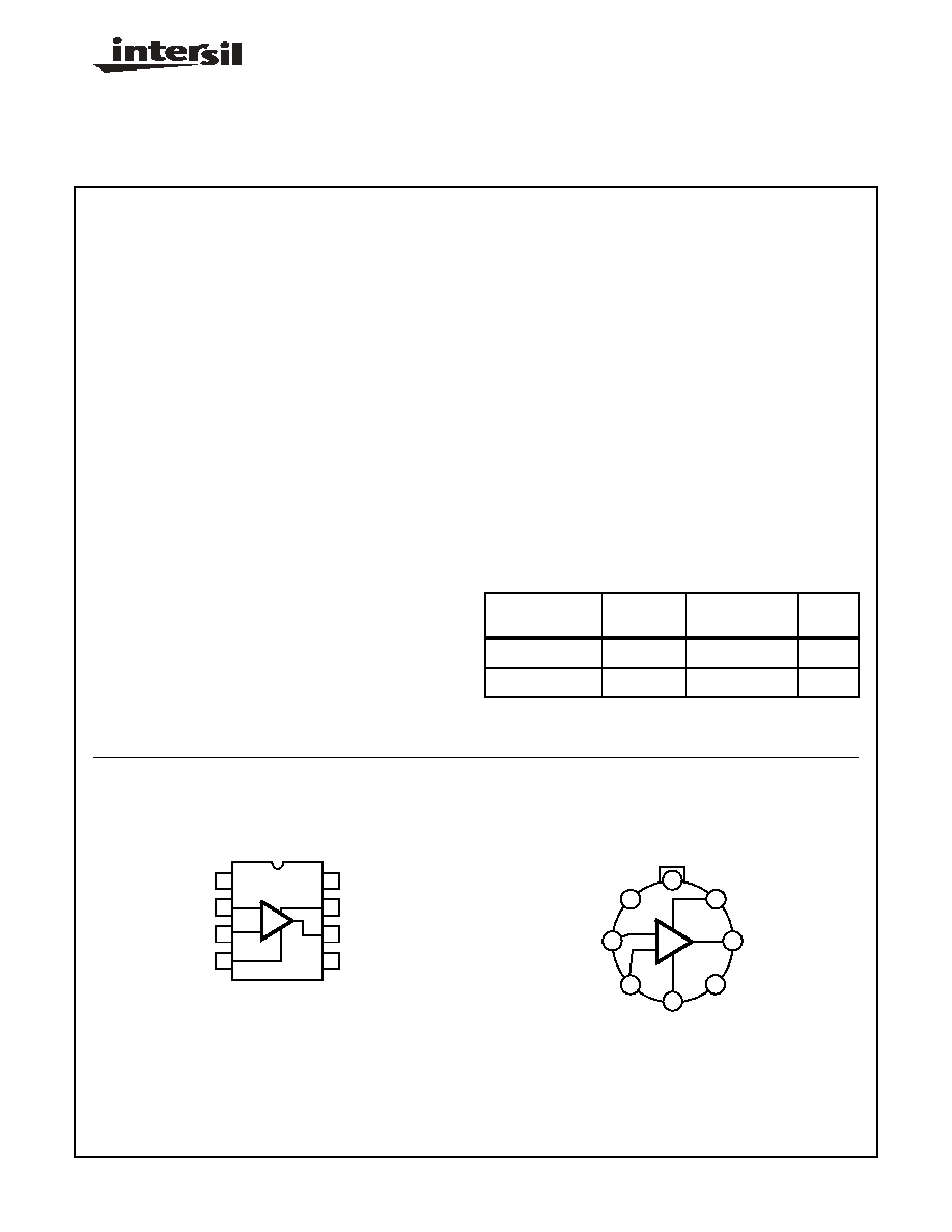
Pinouts
Ordering Information
PART NUMBER
TEMP.
RANGE (
o
C)
PACKAGE
PKG.
NO.
HA2-2510/883
-55 to 125
8 Pin Can
T8.C
HA7-2510/883
-55 to 125
8 Ld CERDIP
F8.3A
HA-2510/883
(CERDIP)
TOP VIEW
HA-2510/883
(METAL CAN)
TOP VIEW
1
2
3
4
8
7
6
5
COMP
V+
OUT
BAL
BAL
-IN
+IN
V-
+
-
2
4
6
1
3
7
5
8
COMP
OUT
-IN
V-
BAL
+IN
V+
BAL
+
-
April 2002
Spec Number
511003-883
FN3697.2
CAUTION: These devices are sensitive to electrostatic discharge; follow proper IC Handling Procedures.
1-888-INTERSIL or 321-724-7143
|
Intersil (and design) is a registered trademark of Intersil Americas Inc.
Copyright © Intersil Americas Inc. 2002. All Rights Reserved
HA-2510/883
High Slew Rate Operational Amplifier
2
Absolute Maximum Ratings
Thermal Information
Voltage Between V+ and V- Terminals . . . . . . . . . . . . . . . . . . . 40V
Differential Input Voltage . . . . . . . . . . . . . . . . . . . . . . . . . . . . . . 15V
Voltage at Either Input Terminal . . . . . . . . . . . . . . . . . . . . . . V+ to V-
Peak Output Current . . . . . . . . . . . . . . . . . . . . . . . . . . . . . . . . 50mA
ESD Rating. . . . . . . . . . . . . . . . . . . . . . . . . . . . . . . . . . . . . . <2000V
Operating Conditions
Temperature Range . . . . . . . . . . . . . . . . . . . . . . . . . -55
o
C to 125
o
C
Supply Voltage
. . . . . . . . . . . . . . . . . . . . . . . . . . . . . . . . . . . . . . . . . ±
15V
V
INCM
1/2 (V+ - V-)
R
L
2k
Thermal Resistance (Typical, Note 1)
JA
JC
CERDIP Package . . . . . . . . . . . . . . . . . . 120
o
C/W
30
o
C/W
Metal Can Package . . . . . . . . . . . . . . . . . 160
o
C/W
75
o
C/W
Package Power Dissipation Limit at 75
o
C for T
J
175
o
C
CERDIP Package . . . . . . . . . . . . . . . . . . . . . . . . . . . . . . . 870mW
Metal Can Package . . . . . . . . . . . . . . . . . . . . . . . . . . . . . . 625mW
Package Power Dissipation Derating Factor Above 75
o
C
CERDIP Package . . . . . . . . . . . . . . . . . . . . . . . . . . . . . 8.7mW/
o
C
Metal Can Package . . . . . . . . . . . . . . . . . . . . . . . . . . . . 6.3mW/
o
C
Maximum Junction Temperature. . . . . . . . . . . . . . . . . . . . . . . 175
o
C
Maximum Storage Temperature Range . . . . . . . . . .-65
o
C to 150
o
C
Maximum Lead Temperature (Soldering 10s). . . . . . . . . . . . . 300
o
C
CAUTION: Stresses above those listed in "Absolute Maximum Ratings" may cause permanent damage to the device. This is a stress only rating and operation
of the device at these or any other conditions above those indicated in the operational sections of this specification is not implied.
NOTE:
1.
JA
is measured with the component mounted on a low effective thermal conductivity test board in free air. See Tech Brief
TB379 for details.
TABLE 1. DC ELECTRICAL PERFORMANCE CHARACTERISTICS
Device Tested at: V
SUPPLY
=
±
15V, R
SOURCE
= 100
, R
LOAD
= 500k
, V
OUT
= 0V, Unless Otherwise Specified.
PARAMETER
SYMBOL
CONDITIONS
GROUP A
SUBGROUPS
TEMP (
o
C)
MIN
MAX
UNITS
Input Offset
Voltage
V
IO
V
CM
= 0V
1
25
-8
8
mV
2, 3
125, -55
-18
10
mV
Input Bias Current
+I
B
V
CM
= 0V, +R
S
= 100k
, -R
S
= 100
1
25
-200
200
nA
2, 3
125, -55
-400
400
nA
-I
B
V
CM
= 0V, +R
S
= 100
, -R
S
= 100k
1
25
-200
200
nA
2, 3
125, -55
-400
400
nA
Input Offset
Current
I
IO
V
CM
= 0V, +R
S
= 100k
, -R
S
= 100k
1
25
-25
25
nA
2, 3
125, -55
-50
50
nA
Common Mode
Range
+CMR
V+ = 5V, V- = -25V
1
25
+10
-
V
2, 3
125, -55
+10
-
V
-CMR
V+ = 25V, V- = -5V
1
25
-
-10
V
2, 3
125, -55
-
-10
V
Large Signal
Voltage Gain
+A
VOL
V
OUT
= 0V and +10V, R
L
= 2k
4
25
10
-
kV/V
5, 6
125, -55
7.5
-
kV/V
-A
VOL
V
OUT
= 0V and -10V, R
L
= 2k
4
25
10
-
kV/V
5, 6
125, -55
7.5
-
kV/V
Common Mode
Rejection Ratio
+CMRR
V
CM
= +10V, V+ = +5V, V- = -25V,
V
OUT
= -10V
1
25
80
-
dB
2, 3
125, -55
80
-
dB
-CMRR
V
CM
= -10V, V+ = +25V, V- = -5V, V
OUT
= +10V
1
25
80
-
dB
2, 3
125, -55
80
-
dB
HA-2510/883
Spec Number
511003-883
3
Output Voltage
Swing
+V
OUT
R
L
= 2k
4
25
10
-
V
5, 6
125, -55
10
-
V
-V
OUT
R
L
= 2k
4
25
-
-10
V
5, 6
125, -55
-
-10
V
Output Current
+I
OUT
V
OUT
= -10V
4
25
10
-
mA
5, 6
125, -55
7.5
-
mA
-I
OUT
V
OUT
= +10V
4
25
-
-10
mA
5, 6
125, -55
-
-7.5
mA
Quiescent Power
Supply Current
+I
CC
V
OUT
= 0V,
I
OUT
= 0mA
1
25
-
6
mA
2, 3
125, -55
-
6.5
mA
-I
CC
V
OUT
= 0V,
I
OUT
= 0mA
1
25
-6
-
mA
2, 3
125, -55
-6.5
-
mA
Power Supply
Rejection Ratio
+PSRR
V
SUP
= 10V, V+ = +20V, V- = -15V,
V+ = +10V, V- = -15V
1
25
80
-
dB
2, 3
125, -55
80
-
dB
-PSRR
V
SUP
= 10V, V+ = +15V, V- = -20V,
V+ = +15V, V- = -10V
1
25
80
-
dB
2, 3
125, -55
80
-
dB
Offset Voltage
Adjustment
+V
IO
Adj
Note 2
1
25
V
IO
-1
-
mV
2, 3
125, -55
V
IO
-1
-
mV
-V
IO
Adj
Note 2
1
25
V
IO
+1
-
mV
2, 3
125, -55
V
IO
+1
-
mV
NOTE:
2. Offset adjustment range is [V
IO
(Measured)
±
1mV] minimum referred to output. This test is for functionality only to assure adjustment
through 0V.
TABLE 2. AC ELECTRICAL PERFORMANCE CHARACTERISTICS
Device Tested at: V
SUPPLY
=
±
15V, R
SOURCE
= 50
, R
LOAD
= 2k
, C
LOAD
= 50pF, A
VCL
= +1V/V, Unless Otherwise Specified.
PARAMETER
SYMBOL
CONDITIONS
GROUP A
SUBGROUPS
TEMP (
o
C)
MIN
MAX
UNITS
Slew Rate
+SR
V
OUT
= -5V to +5V, 25%
+SR
75%
7
25
50
-
V/
µ
s
8A, 8B
125, -55
45
-
V/
µ
s
-SR
V
OUT
= +5V to -5V, 75%
-SR
25%
7
25
50
-
V/
µ
s
8A, 8B
125, -55
45
-
V/
µ
s
TABLE 1. DC ELECTRICAL PERFORMANCE CHARACTERISTICS (Continued)
Device Tested at: V
SUPPLY
=
±
15V, R
SOURCE
= 100
, R
LOAD
= 500k
, V
OUT
= 0V, Unless Otherwise Specified.
PARAMETER
SYMBOL
CONDITIONS
GROUP A
SUBGROUPS
TEMP (
o
C)
MIN
MAX
UNITS
HA-2510/883
Spec Number
511003-883
4
Spec Number
511003-883
Rise and Fall
Time
t
r
V
OUT
= 0 to +200mV, 10%
t
r
90%
7
25
-
50
ns
8A, 8B
125, -55
-
60
ns
t
f
V
OUT
= 0 to -200mV, 10%
t
f
90%
7
25
-
50
ns
8A, 8B
125, -55
-
60
ns
Overshoot
+OS
V
OUT
= 0 to +200mV
7
25
-
40
%
8A, 8B
125, -55
-
50
%
-OS
V
OUT
= 0 to -200mV
7
25
-
40
%
8A, 8B
125, -55
-
50
%
TABLE 3. ELECTRICAL PERFORMANCE CHARACTERISTICS
Device Characterized at: V
SUPPLY
=
±
15V, R
LOAD
= 2k
, C
LOAD
= 50pF, Unless Otherwise Specified.
PARAMETER
SYMBOL
CONDITIONS
NOTES
TEMP (
o
C)
MIN
MAX
UNITS
Differential Input
Resistance
R
IN
V
CM
= 0V
3
25
50
-
M
Full Power
Bandwidth
FPBW
V
PEAK
= 10V
3, 4
25
750
-
kHz
Minimum Closed
Loop Stable Gain
CLSG
R
L
= 2k
, C
L
= 50pF
3
-55 to 125
1
-
V/V
Quiescent Power
Consumption
PC
V
OUT
= 0V, I
OUT
= 0mA
3, 5
-55 to 125
-
195
mW
NOTES:
3. Parameters listed in Table 3 are controlled via design or process parameters and are not directly tested at final production. These param-
eters are lab characterized upon initial design release, or upon design changes. These parameters are guaranteed by characterization
based upon data from multiple production runs which reflect lot to lot and within lot variation.
4. Full Power Bandwidth guarantee based on Slew Rate measurement using FPBW = Slew Rate/(2
V
PEAK
).
5. Quiescent Power Consumption based upon Quiescent Supply Current test maximum. (No load on outputs.)
TABLE 4. ELECTRICAL TEST REQUIREMENTS
MIL-STD-883 TEST REQUIREMENTS
SUBGROUPS (SEE TABLES 1 AND 2)
Interim Electrical Parameters (Pre Burn-In)
1
Final Electrical Test Parameters
1 (Note 6), 2, 3, 4, 5, 6, 7, 8A, 8B
Group A Test Requirements
1, 2, 3, 4, 5, 6, 7, 8A, 8B
Groups C and D Endpoints
1
NOTE:
6. PDA applies to Subgroup 1 only.
TABLE 2. AC ELECTRICAL PERFORMANCE CHARACTERISTICS (Continued)
Device Tested at: V
SUPPLY
=
±
15V, R
SOURCE
= 50
, R
LOAD
= 2k
, C
LOAD
= 50pF, A
VCL
= +1V/V, Unless Otherwise Specified.
PARAMETER
SYMBOL
CONDITIONS
GROUP A
SUBGROUPS
TEMP (
o
C)
MIN
MAX
UNITS
HA-2510/883
5
Die Characteristics
DIE DIMENSIONS:
65 mils x 57 mils x 19 mils
1650
µ
m x 1450
µ
m x 483
µ
m
METALLIZATION:
Type: Al, 1% Cu
Thickness: 16k
≈
±
2k
≈
GLASSIVATION:
Type: Nitride (Si3N4) over Silox (SiO2, 5% Phos.)
Silox Thickness: 12k≈
±
2k≈
Nitride Thickness: 3.5k≈
±
1.5k≈
WORST CASE CURRENT DENSITY:
0.3 x 10
5
A/cm
2
SUBSTRATE POTENTIAL (Powered Up):
Unbiased
TRANSISTOR COUNT:
HA-2510/883: 40
PROCESS: Bipolar Dielectric Isolation
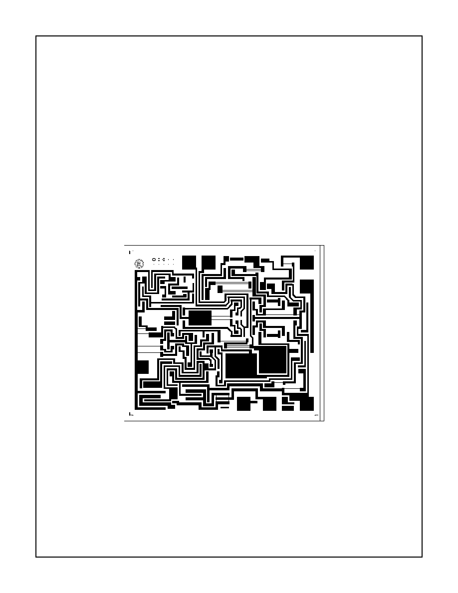
Metallization Mask Layout
HA-2510/883
V-
+IN
OUT
BAL
-IN
V+
COMP
BAL
HA-2510/883