
52
HC-5504B1
ITU Low Cost, PABX SLIC With 40mA
Loop Feed
The Intersil SLIC incorporates many of the BORSHT
functions on a single IC chip. This includes DC battery feed,
a ring relay driver, supervisory and hybrid functions. This
device is designed to maintain transmission performance in
the presence of externally induced longitudinal currents.
Using the unique Intersil dielectric isolation process, the
SLIC can operate directly with a wide range of station
battery voltages.
The SLIC also provides selective denial of power. If the PBX
system becomes overloaded during an emergency, the SLIC
will provide system protection by denying power to selected
subscriber loops.
The Intersil SLIC is ideally suited for the design of new digital
PBX systems by eliminating bulky hybrid transformers.
Pinout
HC-5504B1 (PLCC)
TOP VIEW
Features
∑ Low Cost Version of the HC-5504B
∑ Capable of 5V or 12V (V
B
+) Operation
∑ Monolithic Integrated Device
∑ DI High Voltage Process
∑ Compatible With Worldwide PBX Performance
Requirements
∑ Controlled Supply of Battery Feed Current for Short Loops
(41mA)
∑ Internal Ring Relay Driver
∑ Allows Interfacing With Negative Superimposed Ringing
Systems
∑ Low Power Consumption During Standby
∑ Switch Hook Ground Key and Ring Trip Detection
Functions
∑ Selective Denial of Power to Subscriber Loops
Applications
∑ Solid State Line Interface Circuit for Analog and Digital
PBX Systems
∑ Direct Inward Dial (DID) Trunks
∑ Voice Messaging PBXs
∑ Related Literature
- AN549, The HC-5502S/4X Telephone Subscriber Line
Interface Circuits (SLIC)
- AN571, Using Ring Sync with HC-5502A and HC-5504
SLICs
Ordering Information
PART NUMBER
TEMP.
RANGE (
o
C)
PACKAGE
PKG. NO.
HC4P5504B1-5
0 to 75
28 Ld PLCC
N28.45
C
3
DG
N/C
RS
RD
TF
RX
+IN
N/C
OUT
C
2
RC
RING
TIP
TX
AG
C
4
-IN
RF
BG
N/C
SHD
GKD
PD
V
B
+
N/C
4
5
6
7
8
9
10
11
12
13
14
15
16
17
18
19
20
21
22
23
24
25
26
27
28
1
2
3
RFS
V
B
-
Data Sheet
February 1999
File Number
4125.3
CAUTION: These devices are sensitive to electrostatic discharge; follow proper IC Handling Procedures.
http://www.intersil.com or 407-727-9207
|
Copyright
©
Intersil Corporation 1999
53
Absolute Maximum Ratings
(Note 1)
Thermal Information
Maximum Continuous Supply Voltages
(V
B
-) . . . . . . . . . . . . . . . . . . . . . . . . . . . . . . . . . . . . . . . -60 to 0.5V
(V
B
+) . . . . . . . . . . . . . . . . . . . . . . . . . . . . . . . . . . . . . . -0.5 to 15V
(V
B
+ - V
B
-) . . . . . . . . . . . . . . . . . . . . . . . . . . . . . . . . . . . . . . . .75V
Relay Drive Voltage (V
RD
) . . . . . . . . . . . . . . . . . . . . . . . . -0.5 to 15V
Operating Conditions
Operating Temperature Range
HC-5504B1-5 . . . . . . . . . . . . . . . . . . . . . . . . . . . . . . . 0
o
C to 75
o
C
Relay Driver Voltage (V
RD
) . . . . . . . . . . . . . . . . . . . . . . . . 5V to 12V
Positive Supply Voltage (V
B
+) . . . 4.75V to 5.25V or 10.8V to 13.2V
Negative Supply Voltage (V
B
-). . . . . . . . . . . . . . . . . . . .-42V to -58V
High Level Logic Input Voltage. . . . . . . . . . . . . . . . . . . . . . . . . . 2.4V
Low Level Logic Input Voltage . . . . . . . . . . . . . . . . . . . . . . . . . . 0.6V
Loop Resistance (R
L
) . . . . . . . . . . . . . . . . . . . . . . . .200
to 1200
Thermal Resistance (Typical, Note 2)
JA
(
o
C/W)
28 Lead PLCC . . . . . . . . . . . . . . . . . . . . . . . . . . . . .
65
Maximum Junction Temperature Plastic . . . . . . . . . . . . . . . . .150
o
C
Maximum Storage Temperature Range . . . . . . . . . . -65
o
C to 150
o
C
Maximum Lead Temperature (Soldering 10s) . . . . . . . . . . . . .300
o
C
(PLCC - Lead Tips Only)
Die Characteristics
Transistor Count. . . . . . . . . . . . . . . . . . . . . . . . . . . . . . . . . . . . . . 185
Diode Count. . . . . . . . . . . . . . . . . . . . . . . . . . . . . . . . . . . . . . . . . . 36
Die Dimensions . . . . . . . . . . . . . . . . . . . . . . . . . . . . . . . . . 137 x 102
Substrate Potential. . . . . . . . . . . . . . . . . . . . . . . . . . . . . . Connected
Process . . . . . . . . . . . . . . . . . . . . . . . . . . . . . . . . . . . . . . . Bipolar-DI
CAUTION: Stresses above those listed in "Absolute Maximum Ratings" may cause permanent damage to the device. This is a stress only rating and operation of the
device at these or any other conditions above those indicated in the operational sections of this specification is not implied.
NOTES:
1. Absolute maximum ratings are limiting values, applied individually, beyond which the serviceability of the circuit may be impaired. Functional
operability under any of these conditions is not necessarily implied.
2.
JA
is measured with the component mounted on an evaluation PC board in free air.
Electrical Specifications
Unless Otherwise Specified, V
B
- = -48V, V
B
+ = 12V and 5V, AG = BG = DG = 0V, Typical Parameters
T
A
= 25
o
C. Min-Max Parameters are Over Operating Temperature Range
PARAMETER
CONDITIONS
MIN
TYP
MAX
UNITS
On Hook Power Dissipation
I
LONG
= 0 (Note 2), V
B
+ = 12V
-
170
235
mW
Off Hook Power Dissipation
R
L
= 600
, I
LONG
= 0 (Note 3), V
B
+ = 12V
-
425
550
mW
Off Hook I
B
+
R
L
= 600
, I
LONG
= 0 (Note 3), T
A
= 25
o
C
-
-
5.3
mA
Off Hook I
B
-
R
L
= 600
, I
LONG
= 0 (Note 3)
-
35
41
mA
Off Hook Loop Current
R
L
= 1200
, I
LONG
= 0 (Note 3)
-
21
-
mA
Off Hook Loop Current
R
L
= 1200
, V
B
- = -42V, I
LONG
= 0 (Note 3)
T
A
= 25
o
C
17.5
-
-
mA
Off Hook Loop Current
R
L
= 200
, I
LONG
= 0 (Note 3)
36
41
48
mA
Fault Currents
TIP to Ground
-
14
-
mA
RING to Ground
-
55
-
mA
TIP to RING
-
41
-
mA
TIP and RING to Ground
-
55
-
mA
Ring Relay Drive V
OL
I
OL
= 62mA
-
0.2
0.5
V
Ring Relay Driver Off Leakage
V
RD
= 12V, RC = 1 = HIGH, T
A
= 25
o
C
-
-
100
µ
A
Ring Trip Detection Period
R
L
= 600
-
2
3
Ring
Cycles
Switch Hook Detection Threshold
SHD = V
OL
10
-
-
mA
SHD = V
OH
-
-
5
mA
HC-5504B1
54
Ground Key Detection Threshold
GKD = V
OL
20
-
-
mA
GKD = V
OH
-
-
10
mA
Loop Current During Power Denial
R
L
= 200
-
±
2
-
mA
Dial Pulse Distortion
0
-
5
ms
Receive Input Impedance
(Note 4)
-
110
-
k
Transmit Output Impedance
(Note 4)
-
10
20
2-Wire Return Loss
(Referenced to 600
+ 2.16
µ
F), (Note 4)
SR
L
LO
-
15.5
-
dB
ER
L
-
24
-
dB
SR
L
HI
-
31
-
dB
Longitudinal Balance
1V
RMS
200Hz - 3400Hz, (Note 4) IEEE Method
0
o
C
T
A
75
o
C
2-Wire Off Hook
53
58
-
dB
2-Wire On Hook
53
58
-
dB
4-Wire Off Hook
50
58
-
dB
Low Frequency Longitudinal Balance
R.E.A. Method, (Note 4), R
L
= 600
0
o
C
T
A
75
o
C
-
-
23
dBrnC
-
-
-67
dBm0p
Insertion Loss
At 1kHz, 0dBm Input Level, Referenced 600
2-Wire to 4-Wire, 4-Wire to 2-Wire
-
±
0.05
±
0.2
dB
Frequency Response
200 - 3400Hz Referenced to Absolute Loss at 1kHz
and 0dBm Signal Level (Note 4)
-
±
0.02
±
0.05
dB
Idle Channel Noise
(Note 4)
2-Wire to 4-Wire, 4-Wire to 2-Wire
-
1
5
dBrnC
-
-89
-85
dBm0p
Absolute Delay
(Note 4)
2-Wire to 4-Wire, 4-Wire to 2-Wire
-
-
2
ms
Trans Hybrid Loss
Balance Network Set Up for 600
Termination at
1kHz
30
40
-
dB
Overload Level
V
B
+ = +5V
1.5
-
-
V
PEAK
2-Wire to 4-Wire, 4-Wire to 2-Wire
V
B
+ = 12V
1.75
-
-
V
PEAK
Level Linearity
At 1kHz, (Note 4) Referenced to 0dBm Level
2-Wire to 4-Wire, 4-Wire to 2-Wire
+3 to -40dBm
-
-
±
0.05
dB
-40 to -50dBm
-
-
±
0.1
dB
-50 to -55dBm
-
-
±
0.3
dB
Electrical Specifications
Unless Otherwise Specified, V
B
- = -48V, V
B
+ = 12V and 5V, AG = BG = DG = 0V, Typical Parameters
T
A
= 25
o
C. Min-Max Parameters are Over Operating Temperature Range (Continued)
PARAMETER
CONDITIONS
MIN
TYP
MAX
UNITS
HC-5504B1

55
Power Supply Rejection Ratio
(Note 4)
V
B
+ to 2-Wire
30 - 60Hz, R
L
= 600
15
-
-
dB
V
B
+ to Transmit
15
-
-
dB
V
B
- to 2-Wire
15
-
-
dB
V
B
- to Transmit
15
-
-
dB
V
B
+ to 2-Wire
200 - 16kHz, R
L
= 600
30
-
-
dB
V
B
+ to Transmit
30
-
-
dB
V
B
- to 2-Wire
30
-
-
dB
V
B
- to Transmit
30
-
-
dB
Logic Input Current (RS, RC, PD)
0V
V
IN
5V
-
-
±
100
µ
A
Logic Inputs
Logic `0' V
IL
-
-
0.8
V
Logic `1' V
IH
2.0
-
5.5
V
Logic Outputs
Logic `0' V
OL
I
LOAD
800
µ
A, V
B
+ = 12V, 5V
-
0.1
0.5
V
Logic `1' V
OH
I
LOAD
80
µ
A, V
B
+ = 12V
2.7
5.0
5.5
V
I
LOAD
40
µ
A, V
B
+ = 5V
2.7
-
5.0
V
Uncommitted Op Amp Specifications
PARAMETER
CONDITIONS
MIN
TYP
MAX
UNITS
Input Offset Voltage
-
±
5
-
mV
Input Offset Current
-
±
10
-
nA
Input Bias Current
-
20
-
nA
Differential Input Resistance
(Note 4)
-
1
-
M
Output Voltage Swing
R
L
= 10K, V
B
+ = 12V
-
±
6.2
±
6.6
V
PEAK
R
L
= 10K, V
B
+ = 5V
-
±
3
-
V
PEAK
Output Resistance
A
VCL
= 1 (Note 4)
-
10
-
Small Signal GBW
(Note 4)
-
1
-
MHz
NOTES:
3. I
LONG
= Longitudinal Current
4. These parameters are controlled by design or process parameters and are not directly tested. These parameters are characterized upon initial
design release, upon design changes which would affect these characteristics, and at intervals to assure product quality and specification com-
pliance.
Electrical Specifications
Unless Otherwise Specified, V
B
- = -48V, V
B
+ = 12V and 5V, AG = BG = DG = 0V, Typical Parameters
T
A
= 25
o
C. Min-Max Parameters are Over Operating Temperature Range (Continued)
PARAMETER
CONDITIONS
MIN
TYP
MAX
UNITS
HC-5504B1

56
Pin Descriptions
28 PIN
PLCC
SYMBOL
DESCRIPTION
2
TIP
An analog input connected to the TIP (more positive) side of the subscriber loop through a 150
feed resistor and a ring
relay contact. Functions with the Ring terminal to receive voice signals from the telephone and for loop monitoring pur-
poses.
3
RING
An analog input connected to the RING (more negative) side of the subscriber loop through a 150
feed resistor and a
ring relay contact. Functions with the Tip terminal to receive voice signals from the telephone and for loop monitoring pur-
poses.
4
RFS
Senses ring side of loop for ground key and ring trip detection. During ringing, the ring signal is inserted into the line at
this node and RF is isolated from RFS via a relay.
5
V
B
+
Positive Voltage Source - Most positive supply. V
B
+ is typically 12V or 5V.
6
C
3
Capacitor #3 - An external capacitor to be connected between this terminal and analog ground. Required for proper op-
eration of the loop current limiting function, and for filtering V
B
-. Typical value is 0.3
µ
F, 30V.
7
DG
Digital Ground - To be connected to zero potential and serves as a reference for all digital inputs and outputs on the SLIC
microcircuit.
9
RS
Ring Synchronization Input - A TTL - compatible clock input. The clock should be arranged such that a positive pulse
transition occurs on the zero crossing of the ring voltage source, as it appears at the RFS terminal. For Tip side injected
systems, the RS pulse should occur on the negative going zero crossing and for Ring injected systems, on the positive
going zero crossing. This ensures that the ring relay activates and deactivates when the instantaneous ring voltage is
near zero. If synchronization is not required, the pin should be tied to 5V.
10
RD
Relay Driver - A low active open collector logic output. When enabled, the external ring relay is energized.
11
TF
Tip Feed - A low impedance analog output connected to the TIP terminal through a 150
feed resistor. Functions with
the RF terminal to provide loop current, feed voice signals to the telephone set, and sink longitudinal current.
12
RF
Ring Feed - A low impedance analog output connected to the RING terminal through a 150
feed resistor. Functions with
the TF terminal to provide loop current, feed voice signals to the telephone set, and sink longitudinal current.
13
V
B
-
Negative Voltage Source - Most negative supply. V
B
- is typically -48V with an operational range of -42V to -58V. Frequent-
ly referred to as "battery".
14
BG
Battery Ground - To be connected to zero potential. All loop current and some quiescent current flows into this ground
terminal.
16
SHD
Switch Hook Detection - A low active LS TTL-compatible logic output. This output is enabled for loop currents exceeding
10mA and disabled for loop currents less than 5mA.
17
GKD
Ground Key Detection - A low active LS TTL-compatible logic output. This output is enabled if the DC current into the ring
lead exceeds the DC current out of the tip lead by more than 20mA, and disabled if this current difference is less than
10mA.
18
PD
Power Denial - A low active TTL - Compatible logic input. When enabled, the switch hook detect (SHD) and ground key
detect (GKD) are not necessarily valid, and the relay driver (RD) output is disabled.
19
RC
Ring Command - A low active TTL - Compatible logic input. When enabled, the relay driver (RD) output goes low on the
next high level of the ring sync (RS) input, as long as the SLIC is not in the power denial state (PD = 0) or the subscriber
is not already off- hook (SHD = 0).
20
C
2
Capacitor #2 - An external capacitor to be connected between this terminal and digital ground. Prevents false ground key
indications from occurring during ring trip detection. Typical value is 0.15
µ
F, 10V. This capacitor is not used if ground key
function is not required and (Pin 17) may be left open or connected to digital ground.
21
OUT
The analog output of the spare operational amplifier. The output voltage swing is typically
±
5V.
23
-IN
The inverting analog input of the spare operational amplifier.
24
+IN
The non-inverting analog input of the spare operational amplifier.
25
RX
Receive Input, Four Wire Side - A high impedance analog input which is internally biased. Capacitive coupling to this input
is required. AC signals appearing at this input differentially drive the Tip feed and Ring feed terminals, which in turn drive
tip and ring through 300
of feed resistance on each side of the line.
HC-5504B1

57
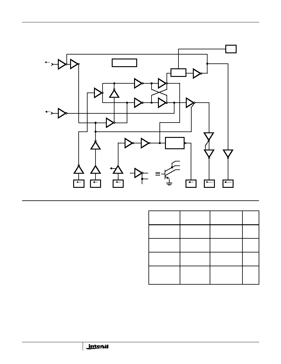
Functional Diagram
26
C
4
Capacitor #4 - An external capacitor to be connected between this terminal and analog ground. This capacitor prevents
false ground key indication and false ring trip detection from occurring when longitudinal currents are induced onto the
subscriber loop from near by power lines and other noise sources. This capacitor is also required for the proper operation
of ring trip detection. Typical value is 0.5
µ
F, to 1.0
µ
F, 20V. This capacitor should be nonpolarized.
27
AG
Analog Ground - To be connected to zero potential and serves as a reference for the transmit output (TX) and receive
input (RX) terminals.
28
TX
Transmit Output, Four Wire Side - A low impedance analog output which represents the differential voltage across Tip
and Ring. Transhybrid balancing must be performed (using the SLIC microcircuit's spare op amp) beyond this output to
completely implement two to four wire conversion. This output is unbalanced and referenced to analog ground. Since the
DC level of this output varies with loop current, capacitive coupling to the next stage is essential.
1, 8,
15, 22
NC
No internal connection.
NOTE: All grounds (AG, BG, and DG) must be applied before V
B
+ or V
B
-. Failure to do so may result in premature failure of the part. If a user wishes
to run separate grounds off a line card, the AG must be applied first.
Pin Descriptions
(Continued)
28 PIN
PLCC
SYMBOL
DESCRIPTION
+
DIFF
AMP
+
OP
AMP
LOOP
MONITORING
RING
CONTROL
2-WIRE
LOOP
SECONDARY
PROTECTION
LINE
DRIVERS
TIP
RING
V
B
-
V
B
-
PD
POWER DENIAL
150
RING
150
RF
BG
150
TF
TIP
RD
RC
RS
RING SYNC
RING COMMAND
RING
TRIP
SHD
GKD
TX
TRANSMIT
OUTPUT
OUT
+IN
-IN
RX
RECEIVE
INPUT
SLIC MICROCIRCUIT
1/2 RING
RELAY
V
B
-
RING
VOLTAGE
RFS
1/2 RING
RELAY
150
SWITCH HOOK
DETECTION
GROUND KEY
DETECTION
-1
+1
BATTERY
FEED
LOOP
CURRENT
LIMITER
HC-5504B1

58
Schematic
SLIC FUNCTIONAL SCHEMATIC
DIP/SOIC Pin Numbers Shown
VB2
VB1
VB2
VB3
VB4
VB5
5V
IB1 IB2 IB3 IB4 IB5 IB6 IB7 IB8
V
BAT
IB9 IB10 IB11
VB+
VB+
A-100
TRANSV'L
I/V AMP
-
+
IB6
R
6
R
5
R
11
V
B
+
R
7
R
8
R
10
R
9
R
22
R
23
R
3
R
4
R
1
R
2
R
16
R
15
VBAT
V
BAT
R
12
V
BAT
VB+
A-200
LONG'L
I / V AMP
IB7
-
+
R
20
V
BAT
V
B
+
A-400
TIP FEED
AMP
IB4
-
+
RING
FEED
SENSE
V
BAT
V
BAT
5V
VB4
IB8
RING TRIP DETECTOR
+
SWITCH HOOK
VB1
IB6
+
R
18
DETECTOR
VB+
QD28
QD27
VBAT
-
+
-
GND SHORTS
CURRENT
LIMITING
IB1
VB3
THERMAL
LIMITING
VB5
STTL
AND LOGIC
INTERFACE
RFC
SH
GK
VB5
-
+
IB2
LOAD CURRENT
LIMITING
R
14
R
13
V
BAT
VBAT/2 REFERENCE
R
21
V
BAT
A-300
RING FEED
AMP
IB5
-
+
RING
RF
TIP
TF
10
2
3
1
9
RX
C
4
V
BAT
BAT
ANA
DIG
V
B
+
GND
GND
GND
21
22
11
12
23
6
4
+
-
OUT
20
19
18
A-500
OP AMP
V
BAT
IB3
VB+
V
B
+
5V IB10
VBAT
PD
15
RC
SHD
GKD
C
2
16
13
17
14
TX
C
3
RS
RD
8
7
24
5
R
17
VB2
VB+
R
19
V
BAT
QD3 QD36
VOLTAGE AND CURRENT
BIAS NETWORK
HC-5504B1
59
Overvoltage Protection and Longitudinal
Current Protection
The SLIC device, in conjunction with an external protection
bridge, will withstand high voltage lightning surges and
power line crosses.
High voltage surge conditions are as specified in Table 1.
The SLIC will withstand longitudinal currents up to a
maximum or 30mA
RMS
, 15mA
RMS
per leg, without any
performance degradation.
LOGIC GATE SCHEMATIC
Schematic
(Continued)
15
5
6
12
4
16
13
A
B
C
C
B
A
TTL
TO
STTL
TTL
TO
STTL
TTL
TO
STTL
TO
R
21
GKD
SHD
RD
PD
RC
RS
C
2
TTL
TO
STTL
TTL
TO
STTL
DELAY
LOGIC BIAS
RELAY
DRIVER
SH
GK
11
14
3
9
7
8
10
2
1
SCHOTTKY LOGIC
TABLE 1.
PARAMETER
TEST
CONDITION
PERFORMANCE
(MAX)
UNITS
Longitudinal
Surge
10
µ
s Rise/
1000
µ
s Fall
±
1000 (Plastic)
V
PEAK
Metallic Surge
10
µ
s Rise/
1000
µ
s Fall
±
1000 (Plastic)
V
PEAK
T/GND
R/GND
10
µ
s Rise/
1000
µ
s Fall
±
1000 (Plastic)
V
PEAK
50/60Hz Current
T/GND
R/GND
11 Cycles
Limited to
10A
RMS
700 (Plastic)
V
RMS
HC-5504B1

60
All Intersil semiconductor products are manufactured, assembled and tested under ISO9000 quality systems certification.
Intersil semiconductor products are sold by description only. Intersil Corporation reserves the right to make changes in circuit design and/or specifications at any time with-
out notice. Accordingly, the reader is cautioned to verify that data sheets are current before placing orders. Information furnished by Intersil is believed to be accurate and
reliable. However, no responsibility is assumed by Intersil or its subsidiaries for its use; nor for any infringements of patents or other rights of third parties which may result
from its use. No license is granted by implication or otherwise under any patent or patent rights of Intersil or its subsidiaries.
For information regarding Intersil Corporation and its products, see web site http://www.intersil.com
Applications Diagram
FIGURE 1.
TYPICAL LINE CIRCUIT APPLICATION WITH THE MONOLITHIC SLIC
Typical Component Values
C
2
= 0.15
µ
F, 10V
C
3
= 0.3
µ
F, 30V
C
4
= 0.5
µ
F to 1.0
µ
F, 10%, 20V (Should be nonpolarized)
C
5
= 0.5
µ
F, 20V
C
6
= C
7
= 0.5
µ
F (10% Match Required) (Note 6)
C
8
= 0.01
µ
F, 100V
C
9
= 0.01
µ
F, 20V,
±
20%
R
1
= R
2
= R
3
= 100k
(0.1% Match Required, 1% absolute
value) Z
B
= 0 for 600
Terminations (Note 6).
R
B1
= R
B2
= R
B3
= R
B4
= 150
(0.1% Match Required, 1%
absolute value).
R
S1
= R
S2
= 1k
, typically.
C
S1
= C
S2
= 0.1
µ
F, 200V typically, depending on V
RING
and
line length.
Z
1
= 150V to 200V transient protection.
PTC used as ring generator ballast.
NOTES:
5. Secondary protection diode bridge recommended is a 2A, 200V type.
6. To obtain the specified transhybrid loss it is necessary for the three legs of the balance network, C
6
-R
1
and R
2
and C
7
-Z
B
-R
3
, to match in im-
pedance to within 0.3%. Thus, if C
6
and C
7
are 1
µ
F each, a 20% match is adequate. It should be noted that the transmit output to C
6
sees a -
22V step when the loop is closed. Too large a value for C
6
may produce an excessively long transient at the op amp output to the PCM Fil-
ter/CODEC.
A 0.5
µ
F and 100k
gives a time constant of 50ms. The uncommitted op amp output is internally clamped to stay within
±
5.5V and also has
current limiting protection.
7. All grounds (AG, BG, and DG) must be applied before V
B
+ or V
B
-. Failure to do so may result in premature failure of the part. If a user wishes
to run separate grounds off a line card, the AG must be applied first.
8. Application shows Ring Injected Ringing, Balanced or Tip injected configuration may be used.
R
B4
K
1B
K
1A
RING
RING FEED
RING FEED SENSE
TIP
V
B
-
SLIC
HC-5504B1
R
S1
R
B2
R
B1
PTC
Z
1
-48V
150V
PEAK
(MAX)
RING GENERATOR
RING
R
B3
R
S2
C
S2
SUBSCRIBER
LOOP
-48V
SYSTEM CONTROLLER
K
1
8
1
9
10
3
2
TIP FEED
TIP
RD
OP AMP
RX
TX
+IN
-IN
OUT
C2
C3
C4
NEG.
BATT.
BATT.
GND.
DIG.
GND.
ANA.
GND.
V
B
+
POWER
DENIAL
SWITCH
HOOK
DETECT
GROUND
KEY
DETECT
RING
SYNC
RING
CMD
15
13
14
7
16
11
12
6
23
C
9
4
V
B
+
C
8
C
4
C
3
C
2
+
+
21
24
20
19
18
17
5
22
C
6
R
1
R
2
C
7
C
5
R
3
BALANCE NETWORK
PCM
FILTER/
CODEC
SWITCHING
NETWORK
Z
B
5V TO
12V
PRIMARY
PROTEC-
TION
C
S1
(NOTE 5)
PIN NUMBERS GIVEN FOR DIP/SOIC PACKAGE.
HC-5504B1