 | –≠–ª–µ–∫—Ç—Ä–æ–Ω–Ω—ã–π –∫–æ–º–ø–æ–Ω–µ–Ω—Ç: HC5503CBZ | –°–∫–∞—á–∞—Ç—å:  PDF PDF  ZIP ZIP |

1
Æ
FN4344.5
HC5503
Low Cost 24V SLIC For PABX / Key
Systems
The Intersil HC5503 low cost SLIC is optimized for use in
small Analog or mixed Analog and Digital Key Telephone
Systems (KTS) or PBX products. The low component count
solution and surface mount package options, enable a small
desktop Key System/PBX product to be achieved. The
internal power dissipation of the end product is minimized by
the low power consumption and minimal power supply
voltage requirements of the HC5503.
The HC5503 integrated solution provides higher quality,
higher reliability and better performance solution than a
transformer, thick film hybrid or discrete analog subscriber
interface design.
The HC5503 is designed in a Dielectrically isolated bipolar
technology and is inherently latch proof and does not require
hot plug or power supply sequencing precautions.
Features
∑ Wide Operating Battery Range (-21V to -44V)
∑ Single Additional +5V Supply
∑ 25mA Short Loop Current Limit
∑ Ring Relay Driver
∑ Switch Hook and Ring Trip Detect
∑ Low On-Hook Power Consumption
∑ On-Hook Transmission
∑ ITU-T Longitudinal Balance Performance
∑ Loop Power Denial Function
∑ Thermal Protection
∑ Supports Tip, Ring or Balanced Ringing Schemes
∑ Low Profile Surface Mount Packaging
∑ Pin Compatible with Industry Standard HC5504B SLIC
∑
Pb-free Available
Applications
∑ Analog Subscriber Line Interfaces in Analog Key Systems
and Digital ISDN PABX Systems
∑ Related Literature
- AN571, Using Ring Sync with HC-5502A and HC-5504
SLICs
Ordering Information
PART NUMBER
TEMP.
RANGE (∞C)
PACKAGE
PKG.
DWG. #
HC5503CB
0 to 75
24 Ld SOIC
M24.3
HC5503CBZ (Note)
0 to 75
24 Ld SOIC
(Pb-free)
M24.3
HC5503CBZ96
(Note)
0 to 75
24 Ld SOIC
(Pb-free)
M24.3
NOTE: Intersil Pb-free products employ special Pb-free material
sets; molding compounds/die attach materials and 100% matte tin
plate termination finish, which is compatible with both SnPb and
Pb-free soldering operations. Intersil Pb-free products are MSL
classified at Pb-free peak reflow temperatures that meet or exceed
the Pb-free requirements of IPC/JEDEC J Std-020B.
Data Sheet
June 2004
CAUTION: These devices are sensitive to electrostatic discharge; follow proper IC Handling Procedures.
1-888-INTERSIL or 321-724-7143
|
Intersil (and design) is a registered trademark of Intersil Americas Inc.
Copyright Harris Corporation 1997-1998, Copyright Intersil Americas Inc. 1999, 2003, 2004. All Rights Reserved
All other trademarks mentioned are the property of their respective owners.
2
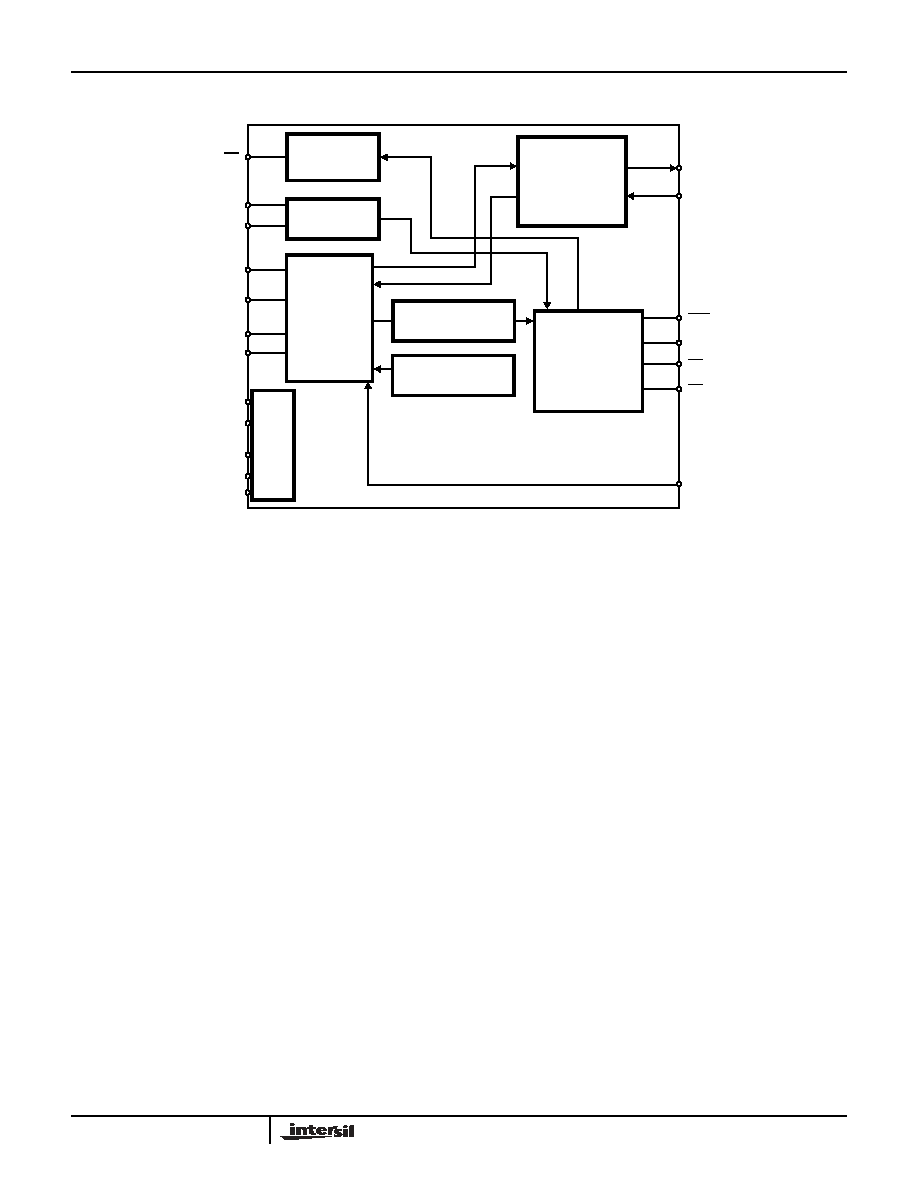
Block Diagram
RD
RFS
TIP
TF
RING
RF
V
BAT
V
CC
BGND
DGND
TX
RX
SHD
RS
RC
PD
RING RELAY
DRIVER
4-WIRE
INTERFACE
VF SIGNAL
PATH
LOOP CURRENT
DETECTOR
BIAS
LOGIC
INTERFACE
RING TRIP
DETECTOR
2-WIRE
INTERFACE
C
1
C2
AGND
THERMAL LIMIT
HC5503

3
Absolute Maximum Ratings
(Note 1)
Thermal Information
Maximum Continuous Supply Voltages
(V
BAT
) . . . . . . . . . . . . . . . . . . . . . . . . . . . . . . . . . . . . . -60 to 0.5V
(V
CC
) . . . . . . . . . . . . . . . . . . . . . . . . . . . . . . . . . . . . . . -0.5 to 15V
(V
CC
- V
BAT
) . . . . . . . . . . . . . . . . . . . . . . . . . . . . . . . . . . . . . .75V
Relay Drive Voltage (V
RD
). . . . . . . . . . . . . . . . . . . . . . . . -0.5 to 15V
Operating Conditions
Operating Temperature Range
HC5503 . . . . . . . . . . . . . . . . . . . . . . . . . . . . . . . . . . . 0∞C to 75∞C
Relay Driver Voltage (V
RD
) . . . . . . . . . . . . . . . . . . . . . . . . 5V to 12V
Positive Supply Voltage (V
CC
). . . . . . . . . . . . . . . . . . 4.75V to 5.25V
Negative Supply Voltage (V
BAT
) . . . . . . . . . . . . . . . . . .-22V to -26V
High Level Logic Input Voltage . . . . . . . . . . . . . . . . . . . . . . . . . 2.4V
Low Level Logic Input Voltage. . . . . . . . . . . . . . . . . . . . . . . . . . 0.6V
Thermal Resistance (Typical, Note 2)
JA
(∞C/W)
24 Lead SOIC . . . . . . . . . . . . . . . . . . . . . . . . . . . . .
75
Maximum Junction Temperature . . . . . . . . . . . . . . . . . . . . . . 150∞C
Maximum Storage Temperature Range . . . . . . . . . . -65∞C to 150∞C
Maximum Lead Temperature (Soldering 10s) . . . . . . . . . . . . . 300∞C
(SOIC - Lead Tips Only)
Die Characteristics
Transistor Count . . . . . . . . . . . . . . . . . . . . . . . . . . . . . . . . . . . . . 185
Diode Count. . . . . . . . . . . . . . . . . . . . . . . . . . . . . . . . . . . . . . . . . . 36
Die Dimensions . . . . . . . . . . . . . . . . . . . . . . . . . . . . . . . . . 137 x 102
Substrate Potential . . . . . . . . . . . . . . . . . . . . . . . . . . . . . Connected
Process . . . . . . . . . . . . . . . . . . . . . . . . . . . . . . . . . . . . . . . Bipolar-DI
CAUTION: Stresses above those listed in "Absolute Maximum Ratings" may cause permanent damage to the device. This is a stress only rating and operation of the
device at these or any other conditions above those indicated in the operational sections of this specification is not implied.
NOTES:
1. Absolute maximum ratings are limiting values, applied individually, beyond which the serviceability of the circuit may be impaired. Functional
operability under any of these conditions is not necessarily implied.
2.
JA
is measured with the component mounted on an evaluation PC board in free air.
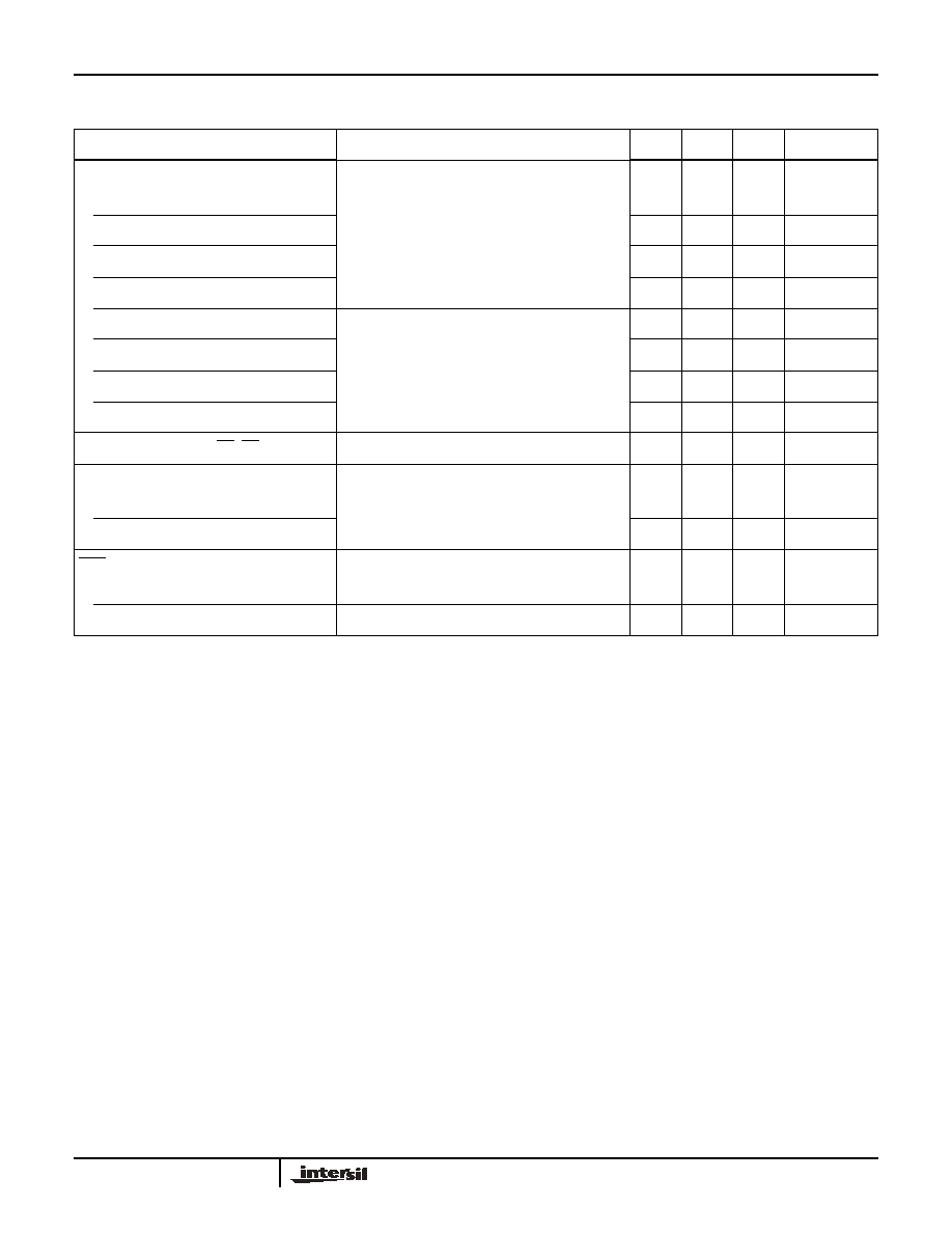
Electrical Specifications
Unless Otherwise Specified, V
BAT
= -24V, V
CC
= 5V, AG = BG = DG = 0V, Typical Parameters
T
A
= 25∞C. Min-Max Parameters are Over Operating Temperature Range.
PARAMETER
CONDITIONS
MIN
TYP
MAX
UNITS
On Hook Power Dissipation
I
LONG
= 0 (Note 3), V
CC
= 5V
-
80
100
mW
Off Hook Power Dissipation
R
L
= 600
, I
LONG
= 0 (Note 4), V
CC
= 5V
-
180
200
mW
Off Hook I
VCC
R
L
= 600
, I
LONG
= 0 (Note 3), T
A
= 0∞C
-
-
6.0
mA
Off Hook I
VCC
R
L
= 600
, I
LONG
= 0 (Note 3), T
A
= 25∞C
-
-
4.0
mA
Off Hook I
BAT
R
L
= 600
, I
LONG
= 0 (Notes 3, 4)
-
19
23
mA
Off Hook Loop Current
R
L
= 400
, I
LONG
= 0 (Note 3)
-
22.9
-
mA
Off Hook Loop Current
R
L
= 400
, V
BAT
= -21.6V, I
LONG
= 0 (Note 3),
T
A
= 25∞C
17.5
-
-
mA
Off Hook Loop Current
R
L
= 200
, I
LONG
= 0 (Note 3)
-
25
30
mA
Fault Currents
TIP to Ground
(Note 4)
-
27.5
-
mA
RING to Ground
-
70
-
mA
TIP to RING
(Note 4)
-
30
-
mA
TIP and RING to Ground
-
140
-
mA
Ring Relay Drive V
OL
I
OL
= 62mA
-
0.2
0.5
V
Ring Relay Driver Off Leakage
V
RD
= 12V, RC = 1 = HIGH, T
A
= 25∞C
-
-
25
µ
A
Ring Trip Detection Period
R
L
= 600
,
(Note 5)
-
2
3
Ring Cycles
Switch Hook Detection Threshold
5
-
10.5
mA
Loop Current During Power Denial
R
L
= 200
-
±
2
-
mA
HC5503

4
Dial Pulse Distortion
(Note 4)
0
-
0.5
ms
Receive Input Impedance
(Note 5)
-
90
-
k
Transmit Output Impedance
(Note 5)
-
10
20
2-Wire Return Loss
Referenced to 600
+2.16
µ
F (Note 4)
SR
L
LO
-
15.5
-
dB
ER
L
-
24
-
dB
SR
L
HI
-
31
-
dB
Longitudinal Balance
1V
RMS
200Hz - 3400Hz, (Note 4) IEEE Method
0∞C
T
A
75∞C
2-Wire Off Hook
53
58
-
dB
2-Wire On Hook
53
58
-
dB
4-Wire Off Hook at 1kHz
50
58
-
dB
Insertion Loss
0dBm Input Level, Referenced 600
2-Wire to 4-Wire at 3.4kHz
V
TR
to V
O
V
O
is the Output of the Transhybrid
Amplifier
-
±
0.05
±
0.2
dB
4-Wire to 2-Wire at 300Hz
-3.8
-4.0
-4.2
dB
Frequency Response
200 - 3400Hz Referenced to Absolute Loss at 1kHz
and 0dBm Signal Level (Note 4)
-
±
0.02
±
0.05
dB
Idle Channel Noise,
2-Wire to 4-Wire
-
1
5
dBrnC
-
-89
-85
dBm0p
Idle Channel Noise,
4-Wire to 2-Wire
(Note 4)
-
1
5
dBrnC
-
-89
-85
dBm0p
Absolute Delay
(Note 5)
2-Wire to 4-Wire, 4-Wire to 2-Wire
-
-
2
µ
s
Trans Hybrid Loss
Balance Network Set Up for 600
Termination at
1kHz
30
40
-
dB
Overload Level
V
CC
= +5V
2-Wire to 4-Wire (On-hook)
2.5
-
-
V
PEAK
4-Wire to 2-Wire (Off-hook, R
L
= 600
)
3.1
-
-
V
PEAK
Level Linearity
At 1kHz, (Note 4) Referenced to 0dBm Level
2-Wire to 4-Wire, 4-Wire to 2-Wire
+3 to -40dBm
-
-
±
0.05
dB
-40 to -50dBm
-
-
±
0.1
dB
-50 to -55dBm
-
-
±
0.3
dB
Electrical Specifications
Unless Otherwise Specified, V
BAT
= -24V, V
CC
= 5V, AG = BG = DG = 0V, Typical Parameters
T
A
= 25∞C. Min-Max Parameters are Over Operating Temperature Range. (Continued)
PARAMETER
CONDITIONS
MIN
TYP
MAX
UNITS
HC5503
5
Power Supply Rejection Ratio
(Note 4),
30 - 60Hz, R
L
= 200
V
CC
to 2-Wire
35
-
-
dB
V
CC
to Transmit
35
-
-
dB
V
BAT
to 2-Wire
20
-
-
dB
V
BAT
to Transmit
20
-
-
dB
V
CC
to 2-Wire
200 - 16kHz, R
L
= 200
35
-
-
dB
V
CC
to Transmit
35
-
-
dB
V
BAT
to 2-Wire
35
-
-
dB
V
BAT
to Transmit
35
-
-
dB
Logic Input Current (RS, RC, PD)
0V
V
IN
2.4V
-
-
±
20
µ
A
Logic Inputs
Logic `0' V
IL
-
-
0.8
V
Logic `1' V
IH
2.0
-
5.5
V
SHD Output
I
LOAD
800
µ
A, V
CC
= 5V
Logic `0' V
OL
-
0.1
0.4
V
Logic `1' V
OH
I
LOAD
40
µ
A, V
CC
= 5V
2.7
-
5.0
V
NOTES:
3. I
LONG
= Longitudinal Current.
4. These parameters are controlled by design or process parameters and are not directly tested. These parameters are characterized upon initial
design release, upon design changes which would affect these characteristics, and at intervals to assure product quality and specification
compliance.
5. Guaranteed by design, not tested.
Electrical Specifications
Unless Otherwise Specified, V
BAT
= -24V, V
CC
= 5V, AG = BG = DG = 0V, Typical Parameters
T
A
= 25∞C. Min-Max Parameters are Over Operating Temperature Range. (Continued)
PARAMETER
CONDITIONS
MIN
TYP
MAX
UNITS
HC5503