
1
Æ
FN4806.1
CAUTION: These devices are sensitive to electrostatic discharge; follow proper IC Handling Procedures.
1-888-INTERSIL or 321-724-7143
|
Intersil (and design) is a registered trademark of Intersil Americas Inc.
Copyright © Intersil Americas Inc. 2003. All Rights Reserved
All other trademarks mentioned are the property of their respective owners.
HC5503PRC
Low Cost SLIC For Large Telecom
Switches
The HC5503PRC is a low cost SLIC optimized for large
Telecom switches. It combines a flexible voltage feed
architecture with the Intersil latch-free DI bonded wafer
process, to provide a low component count, carrier class
solution at very low cost. The re-configurable design permits
simple, economical solutions for campus-wide call center
and PBX applications. External components can be used in
conjunction with the high battery voltage capability to meet
the complex impedance and long loop drive requirements of
Central Office switches, worldwide.
Features
∑ Wide Operating Battery Range (-40V to -58V)
∑ Single Additional +5V Supply
∑ 30mA Short Loop Current Limit
∑ Ring Relay Driver
∑ Switch Hook and Ring Trip Detect
∑ Low On-Hook Power Consumption
∑ On-Hook Transmission
∑ ITU-T Longitudinal Balance Performance
∑ Loop Power Denial Function
∑ Thermal Protection
∑ Supports Tip, Ring or Balanced Ringing Schemes
∑ Low Profile SO, PLCC, and QFN Surface Mount
Packaging
Applications
∑ Central Office, PBX, Call Centers
∑ Related Literature
- AN571, Using Ring Sync with HC-5502A and HC-5504
SLICs
Block Diagram
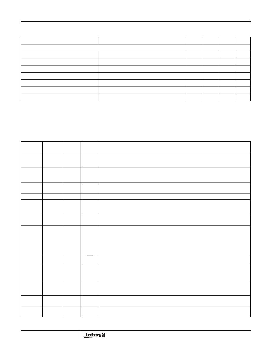
Ordering Information
PART NUMBER
TEMP.
RANGE (
o
C)
PACKAGE
PKG. NO.
HC5503PRCM
0 to 70
28 Ld PLCC
N28.45
HC5503PRCB
0 to 70
24 Ld SOIC
M24.3
HC5503PRCR
0 to 70
32 Ld QFN 7 X 7
L32.7X7A
RD
RFS
TIP
TF
RING
RF
V
BAT
V
CC
BGND
DGND
TX
RX
SHD
RS
RC
PD
RING RELAY
DRIVER
4-WIRE
INTERFACE
VF SIGNAL
PATH
LOOP CURRENT
DETECTOR
BIAS
LOGIC
INTERFACE
RING TRIP
DETECTOR
2-WIRE
INTERFACE
C1
C
2
AGND
THERMAL LIMIT
-
+
OUT
+IN
-IN
Data Sheet
February 2003

2
Absolute Maximum Ratings
Thermal Information
Maximum Continuous Supply Voltages
(V
B
-) . . . . . . . . . . . . . . . . . . . . . . . . . . . . . . . . . . . . . . . -60 to 0.5V
(V
B
+) . . . . . . . . . . . . . . . . . . . . . . . . . . . . . . . . . . . . . . . -0.5 to 7V
(V
B
+ - V
B
-) . . . . . . . . . . . . . . . . . . . . . . . . . . . . . . . . . . . . . . . .75V
Relay Drive Voltage (V
RD
). . . . . . . . . . . . . . . . . . . . . . . . -0.5 to 15V
Operating Conditions
Operating Temperature Range . . . . . . . . . . . . . . . . . . . 0
o
C to 70
o
C
Relay Driver Voltage (V
RD
) . . . . . . . . . . . . . . . . . . . . . . . . 5V to 12V
Positive Supply Voltage (V
B
+) . . . . . . . . . . . . . . . . . . 4.75V to 5.25V
Negative Supply Voltage (V
B
-) . . . . . . . . . . . . . . . . . . .-40V to -58V
High Level Logic Input Voltage . . . . . . . . . . . . . . . . . . . . . . . . . 2.4V
Low Level Logic Input Voltage. . . . . . . . . . . . . . . . . . . . . . . . . . 0.6V
Subscriber Loop Resistance . . . . . . . . . . . . . . . . . . . 200
- 1800
Thermal Resistance (Typical, Note 2, 3)
JA
(
o
C/W)
24 Lead SOIC . . . . . . . . . . . . . . . . . . . . . . . . . . . . .
75
28 Lead PLCC . . . . . . . . . . . . . . . . . . . . . . . . . . . . .
65
32 Lead 7x7 QFN . . . . . . . . . . . . . . . . . . . . . . . . . .
32
Maximum Junction Temperature Plastic . . . . . . . . . . . . . . . . .150
o
C
Maximum Storage Temperature Range . . . . . . . . . -65
o
C to 150
o
C
Maximum Lead Temperature (Soldering 10s) . . . . . . . . . . . . .300
o
C
(PLCC and SOIC - Lead Tips Only)
Die Characteristics
Transistor Count . . . . . . . . . . . . . . . . . . . . . . . . . . . . . . . . . . . . . 185
Diode Count. . . . . . . . . . . . . . . . . . . . . . . . . . . . . . . . . . . . . . . . . . 36
Die Dimensions . . . . . . . . . . . . . . . . . . . . . . . . . . . . . . . . . 137 x 102
Substrate Potential . . . . . . . . . . . . . . . . . . . . . . . . . . . . . Connected
Process . . . . . . . . . . . . . . . . . . . . . . . . . . . . . . . . . . . . . . . Bipolar-DI
CAUTION: Stresses above those listed in "Absolute Maximum Ratings" may cause permanent damage to the device. This is a stress only rating and operation of the
device at these or any other conditions above those indicated in the operational sections of this specification is not implied.
NOTES:
1. Absolute maximum ratings are limiting values, applied individually, beyond which the serviceability of the circuit may be impaired. Functional
operability under any of these conditions is not necessarily implied.
2.
JA
is measured with the component mounted on an evaluation PC board in free air.
3.
JA
for the QFN package is measured in free air with the component mounted on a high effective thermal conductivity test board with direct
attach features including conductive thermal vias. See Tech Brief TB379 and TB389 for additional information and board layout consideration
Electrical Specifications
Unless Otherwise Specified, V
B
- = -48V, V
B
+ = 5V, AG = BG = DG = 0V, R
P
= 50
, R
S
= 100
, Typical
Parameters. T
A
= 25
o
C. Min-Max Parameters are Over Operating Temperature Range
PARAMETER
CONDITIONS
MIN
TYP
MAX
UNITS
On Hook Power Dissipation
I
LONG
= 0 (Note 4)
-
113
-
mW
Off Hook Power Dissipation
R
L
= 600
, I
LONG
= 0 (Notes 3, 4)
-
750
-
mW
On Hook I
B
+
R
L
=
, I
LONG
= 0
-
1.4
-
mA
Off Hook I
B
+
R
L
= 600
, I
LONG
= 0
-
2.8
-
mA
On Hook I
B
-
R
L
=
, I
LONG
= 0
-
2.2
-
mA
Off Hook I
B
-
R
L
= 600
, I
LONG
= 0
-
31
-
mA
Off Hook Loop Current
R
L
= 1800
(I
LOOP
= 0)
18
-
-
mA
Off Hook Loop Current
R
L
= 200
, I
LONG
= 0 (Note 3)
25
30
35
mA
Fault Currents
TIP to Ground
-
27
-
mA
RING to Ground
-
55
-
mA
TIP to RING
-
30
-
mA
TIP and RING to Ground
-
69
-
mA
Ring Relay Drive V
OL
I
OL
= 62mA
-
0.2
0.5
V
Ring Relay Driver Off Leakage
V
RD
= 12V, RC = 1 = HIGH, T
A
= 25
o
C
-
-
100
µ
A
DC Ring Trip Threshold
8.1
10.8
13.5
mA
Switch Hook Detection Threshold
5.0
7.5
10
mA
Loop Current During Power Denial
R
L
= 200
-
3.2
-
mA
Dial Pulse Distortion
(Note 4)
0
-
0.5
ms
Receive Input Impedance
(Note 4)
-
110
-
k
Transmit Output Impedance
(Note 4)
-
10
20
HC5503PRC

3
2-Wire Return Loss
(Referenced to 600
+ 2.16
µ
F), R
P
= R
S
= 150
(Note 4)
SR
L
LO
-
15.5
-
dB
ER
L
-
24
-
dB
SR
L
HI
-
31
-
dB
Longitudinal Balance
1V
RMS
200Hz - 3400Hz, (Note 4) IEEE Method
0
o
C
T
A
75
o
C, R
P
= R
S
= 150
2-Wire Off Hook (Note 4)
53
58
-
dB
2-Wire On Hook (Note 4)
53
58
-
dB
4-Wire Off Hook
50
58
-
dB
Insertion Loss
At 1kHz, 0dBm Input Level, Referenced 600
,
R
P
= R
S
= 150
2-Wire to 4-Wire, 4-Wire to 2-Wire
-
±
0.05
±
0.2
dB
Frequency Response
200 - 3400Hz Referenced to Absolute Loss at 1kHz and
0dBm Signal Level, R
P
= R
S
= 150
(Note 4)
-
±
0.02
±
0.05
dB
Idle Channel Noise
R
P
= R
S
= 150
(Note 4)
2-Wire to 4-Wire, 4-Wire to 2-Wire
-
1
5
dBrnC
-
-89
-85
dBm0p
Absolute Delay
R
P
= R
S
= 150
(Note 4)
2-Wire to 4-Wire, 4-Wire to 2-Wire
-
-
2
µ
s
Trans Hybrid Loss
Balance Network Set Up for 600
Termination at 1kHz,
R
P
= R
S
= 150
(Note 4)
30
40
-
dB
Overload Level
V
B
+ = +5V, R
P
= R
S
= 150
(Note 4)
2-Wire to 4-Wire, 4-Wire to 2-Wire
1.5
-
-
V
PEAK
Level Linearity
2-Wire to 4-Wire, 4-Wire to 2-Wire (Note 4)
At 1kHz, (Note 4) Referenced to 0dBm Level,
R
P
= R
S
= 150
+3 to -40dBm
-
-
±
0.05
dB
-40 to -50dBm
-
-
±
0.1
dB
-50 to -55dBm
-
-
±
0.3
dB
Power Supply Rejection Ratio
R
P
= R
S
= 150
(Note 4)
30 - 60Hz, R
L
= 600
V
B
+ to 2-Wire
15
-
-
dB
V
B
+ to Transmit
15
-
-
dB
V
B
- to 2-Wire
15
-
-
dB
V
B
- to Transmit
15
-
-
dB
V
B
+ to 2-Wire
200 - 16kHz, R
L
= 600
,
R
P
= R
S
= 150
30
-
-
dB
V
B
+ to Transmit
30
-
-
dB
V
B
- to 2-Wire
30
-
-
dB
V
B
- to Transmit
30
-
-
dB
Logic Input Current (RS, RC, PD)
0V
V
IN
5V
-
-
±
100
µ
A
Logic Inputs
Logic `0' V
IL
-
-
0.8
V
Logic `1' V
IH
2.0
-
5.5
V
Logic Outputs
Logic `0' V
OL
I
LOAD
800
µ
A, V
B
+ = 5V
-
0.1
0.5
V
Logic `1' V
OH
I
LOAD
40
µ
A, V
B
+ = 5V
2.7
-
5.0
V
Electrical Specifications
Unless Otherwise Specified, V
B
- = -48V, V
B
+ = 5V, AG = BG = DG = 0V, R
P
= 50
, R
S
= 100
, Typical
Parameters. T
A
= 25
o
C. Min-Max Parameters are Over Operating Temperature Range (Continued)
PARAMETER
CONDITIONS
MIN
TYP
MAX
UNITS
HC5503PRC
4
UNCOMMITTED OP AMP SPECIFICATIONS
Input Offset Voltage
-
±
5
-
mV
Input Offset Current
-
±
10
-
nA
Input Bias Current
-
20
-
nA
Differential Input Resistance
(Note 4)
-
1
-
M
Output Voltage Swing
R
L
= 10K, V
B
+ = 5V
-
±
3
-
V
PEAK
Output Resistance
A
VCL
= 1 (Note 4)
-
10
-
Small Signal GBW
(Note 4)
-
1
-
MHz
NOTES:
4. I
LONG
= Longitudinal Current.
5. These parameters are controlled by design or process parameters and are not directly tested. These parameters are characterized upon initial
design release, upon design changes which would affect these characteristics, and at intervals to assure product quality and specification
compliance.
Electrical Specifications
Unless Otherwise Specified, V
B
- = -48V, V
B
+ = 5V, AG = BG = DG = 0V, R
P
= 50
, R
S
= 100
, Typical
Parameters. T
A
= 25
o
C. Min-Max Parameters are Over Operating Temperature Range (Continued)
PARAMETER
CONDITIONS
MIN
TYP
MAX
UNITS
Pin Descriptions
28 PIN
PLCC
24 PIN
DIP/SOIC
7 x 7
QFN
SYMBOL
DESCRIPTION
2
1
28
TIP
An analog input connected to the TIP (more positive) side of the subscriber loop through a sense
resistor (R
S
) and a ring relay contact. Functions with the Ring terminal to receive voice signals
from the telephone and for loop monitoring purposes.
3
2
31
RING
An analog input connected to the RING (more negative) side of the subscriber loop through a
sense resistor (R
S
) and a ring relay contact. Functions with the Tip terminal to receive voice
signals from the telephone and for loop monitoring purposes.
4
3
32
RFS
Senses ring side of loop for ground key and ring trip detection. During ringing, the ring signal is
inserted into the line at this node and RF is isolated from RFS via a relay.
5
4
1
V
B
+
Positive Voltage Source - Most positive supply. V
B
+ is typically.
6
5
3
C
1
Capacitor #1 - An external capacitor to be connected between this terminal and analog ground.
Required for proper operation of the loop current limiting function, and for filtering V
B
-. Typical
value is 0.3
µ
F, 30V.
7
6
4
DG
Digital Ground - To be connected to zero potential and serves as a reference for all digital inputs
and outputs on the SLIC microcircuit.
9
7
5
RS
Ring Synchronization Input - A TTL - compatible clock input. The clock should be arranged such
that a positive pulse transition occurs on the zero crossing of the ring voltage source, as it
appears at the RFS terminal. For Tip side injected systems, the RS pulse should occur on the
negative going zero crossing and for Ring injected systems, on the positive going zero crossing.
This ensures that the ring relay activates and deactivates when the instantaneous ring voltage
is near zero. If synchronization is not required, the pin should be tied to 5V.
10
8
6
RD
Relay Driver - A low active open collector logic output. When enabled, the external ring relay is
energized.
11
9
7, 8
TF
Tip Feed - A low impedance analog output connected to the TIP terminal through a sense
resistor (R
S
). Functions with the RF terminal to provide loop current, feed voice signals to the
telephone set, and sink longitudinal current.
12
10
9, 10
RF
Ring Feed - A low impedance analog output connected to the RING terminal through a sense
resistor (R
S
). Functions with the TF terminal to provide loop current, feed voice signals to the
telephone set, and sink longitudinal current.
13
11
11
V
B
-
Negative Voltage Source - Most negative supply. V
B
- is typically -48V with an operational range
of -42V to -58V. Frequently referred to as "battery".
14
12
12
BG
Battery Ground - To be connected to zero potential. All loop current and some quiescent current
flows into this ground terminal.
HC5503PRC

5
16
13
13
SHD
Switch Hook Detection - A low active LS TTL - compatible logic output. This output is enabled
for loop currents exceeding the switch hook threshold.
17
14
14,19
NC
Used during production test. Leave disconnected.
18
15
15
PD
Power Denial - A low active TTL - Compatible logic input. When enabled, the ring feed voltage
collapses to the tip feed voltage (~4V). The DC feed is disabled, but the AC transmission is
maintained. The switch hook detect (SHD) is not necessarily valid, and the relay driver (RD)
output is disabled.
19
16
16
RC
Ring Command - A low active TTL - Compatible logic input. When enabled, the relay driver (RD)
output goes low on the next high level of the ring sync (RS) input, as long as the SLIC is not in
the power denial state (PD = 0) or the subscriber is not already off- hook (SHD = 0).
20
17
NC
Leave disconnected.
21
18
20
OUT
The analog output of the spare operational amplifier.
23
19
21
-IN
The inverting analog input of the spare operational amplifier.
24
20
22
+IN
The non-inverting analog input of the spare operational amplifier.
25
21
23
RX
Receive Input, Four Wire Side - A high impedance analog input which is internally biased.
Capacitive coupling to this input is required. AC signals appearing at this input differentially drive
the Tip feed and Ring feed terminals.
26
22
25
C
2
Capacitor #2 - An external capacitor to be connected between this terminal and analog ground.
This capacitor is required for the proper operation of ring trip detection. Recommended value
0.82
µ
F
±
10% 10V non-polarized.
27
23
26
AG
Analog Ground - To be connected to zero potential and serves as a reference for the transmit
output (TX) and receive input (RX) terminals.
28
24
27
TX
Transmit Output, Four Wire Side - A low impedance analog output proportional to the loop
current. Transhybrid balancing must be performed beyond this output to completely implement
two to four wire conversion. This output is unbalanced and referenced to analog ground. Since
the DC level of this output varies with loop current, capacitive coupling to the next stage is
essential.
1, 8, 15, 22
2, 17,
18,24, 29,
30,
NC
No internal connection.
NOTE: All grounds (AG, BG, and DG) must be applied before V
B
+ or V
B
-. Failure to do so may result in premature failure of the part. If a user wishes
to run separate grounds off a line card, the AG must be applied first.
Pin Descriptions
(Continued)
28 PIN
PLCC
24 PIN
DIP/SOIC
7 x 7
QFN
SYMBOL
DESCRIPTION
HC5503PRC
6
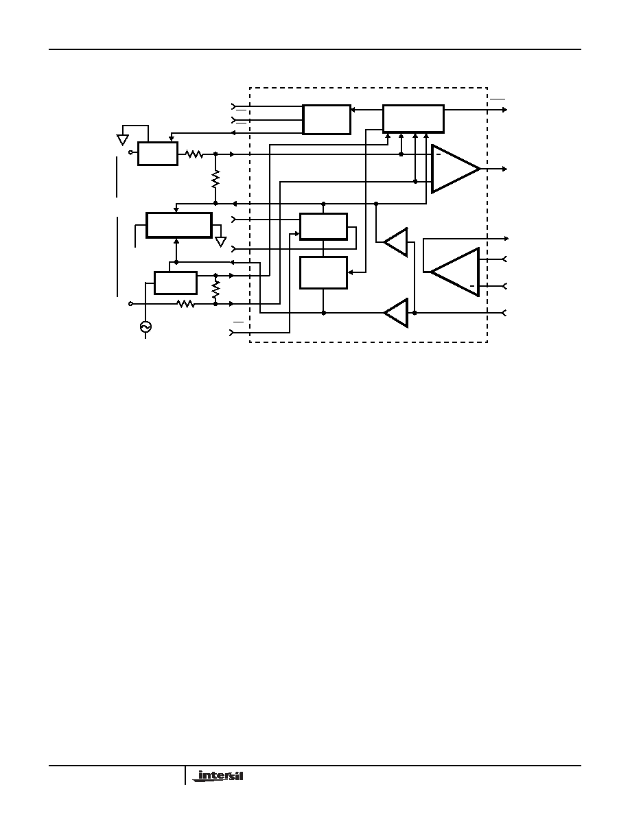
Functional Diagram
+
DIFF
AMP
+
OP
AMP
LOOP
MONITORING
RING
CONTROL
2-WIRE
LOOP
SECONDARY
PROTECTION
LINE
DRIVERS
TIP
RING
V
B
-
V
B
-
PD
POWER DENIAL
R
P
RING
R
S
RF
BG
TF
TIP
RD
RC
RS
RING SYNC
RING COMMAND
RING
TRIP
SHD
TX
TRANSMIT
OUTPUT
OUT
+IN
-IN
RX
RECEIVE
INPUT
SLIC MICROCIRCUIT
1/2 RING
RELAY
V
B
-
RING
VOLTAGE
RFS
1/2 RING
RELAY
R
S
SWITCH HOOK
DETECTION
-1
+1
BATTERY
FEED
LOOP
CURRENT
LIMITER
R
P
R
S
: 100
; 1/2W to 2W depending on surge requirements
R
P
: 50
; 1/2W to 2W depending on surge requirements
HC5503PRC
7
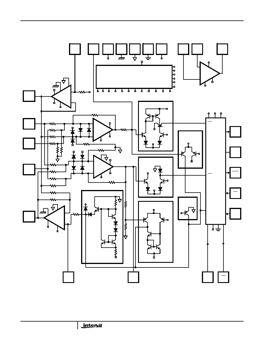
SLIC FUNCTIONAL SCHEMATIC
SOIC PIN NUMBERS SHOWN
V
B2
V
B1
V
B2
V
B3
V
B4
V
B5
5V
I
B1
I
B2
I
B3
I
B4
I
B5
I
B6
I
B7
I
B8
V
BAT
I
B9
I
B10
I
B11
V
B
+
V
B
+
A-100
TRANSV'L
I/V AMP
-
+
I
B6
R
6
R
5
R
11
V
B
+
R
7
R
8
R
10
R
9
R
22
R
23
R
3
R
4
R
1
R
2
R
16
R
15
V
BAT
V
BAT
R
12
V
BAT
V
B
+
A-200
LONG'L
I/V AMP
I
B7
-
+
R
20
V
BAT
V
B
+
A-400
TIP FEED
AMP
I
B4
-
+
RING
FEED
SENSE
V
BAT
V
BAT
5V
V
B4
I
B8
RING TRIP DETECTOR
+
SWITCH HOOK
V
B1
I
B6
+
R
18
DETECTOR
V
B
+
Q
D28
Q
D27
V
BAT
-
+
-
GND SHORTS
CURRENT
LIMITING
I
B1
V
B3
THERMAL
LIMITING
V
B5
STTL
AND LOGIC
INTERFACE
RFC
SH
GK
V
B5
-
+
I
B2
LOAD CURRENT
LIMITING
R
14
R
13
V
BAT
V
BAT/2
REFERENCE
R
21
V
BAT
A-300
RING FEED
AMP
I
B5
-
+
RING
RF
TIP
TF
10
2
3
1
9
RX
C2
V
BAT
BAT
ANA
DIG
V
B
+
GND
GND
GND
21
22
11
12
23
6
4
+
-
OUT
20
19
18
A-500
OP AMP
V
BAT
I
B3
V
B
+
V
B
+
5V I
B10
V
BAT
PD
15
RC
SHD
NC
NC
16
13
17
14
TX
C1
RS
RD
8
7
24
5
R
17
V
B2
V
B
+
R
19
V
BAT
Q
D3
Q
D36
VOLTAGE AND CURRENT
BIAS NETWORK
HC5503PRC

8
Surge Protection
The SLIC device, in conjunction with an external protection
bridge, will withstand high voltage lightning surges and
power line crosses.
The voltage withstand capability of pins `Tip', `Ring' and
`RFs' is
±
450V with respect to ground, as shown in Table 1.
This device is intended for use with an appropriate
secondary protection circuit scheme.
The SLIC will withstand longitudinal currents up to a
maximum or 30mA
RMS
, 15mA
RMS
per leg, without any
performance degradation.
LOGIC GATE SCHEMATIC
15
5
6
12
4
16
13
A
B
C
C
B
A
TTL
TO
STTL
TTL
TO
STTL
TTL
TO
STTL
TO
R
21
SHD
RD
PD
RC
RS
TTL
TO
STTL
DELAY
LOGIC BIAS
RELAY
DRIVER
SH
GK
11
14
3
9
7
8
10
2
1
SCHOTTKY LOGIC
TABLE 1.
PARAMETER
TEST
CONDITION
PERFORMANCE
(MAX)
UNITS
Longitudinal Surge 10
µ
s Rise/
1000
µ
s Fall
±
450 (Plastic)
V
PEAK
Metallic Surge
10
µ
s Rise/
1000
µ
s Fall
±
450 (Plastic)
V
PEAK
T/GND
R/GND
10
µ
s Rise/
1000
µ
s Fall
±
450 (Plastic)
V
PEAK
50/60Hz Current
T/GND
R/GND
11 Cycles
Limited to
10A
RMS
315 (Plastic)
V
RMS
HC5503PRC
9
HC5503PRC
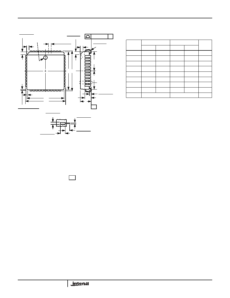
Plastic Leaded Chip Carrier Packages (PLCC)
NOTES:
1. Controlling dimension: INCH. Converted millimeter dimensions are
not necessarily exact.
2. Dimensions and tolerancing per ANSI Y14.5M-1982.
3. Dimensions D1 and E1 do not include mold protrusions. Allowable
mold protrusion is 0.010 inch (0.25mm) per side. Dimensions D1
and E1 include mold mismatch and are measured at the extreme
material condition at the body parting line.
4. To be measured at seating plane
contact point.
5. Centerline to be determined where center leads exit plastic body.
6. "N" is the number of terminal positions.
-C-
A1
A
SEATING
PLANE
0.020 (0.51)
MIN
VIEW "A"
D2/E2
0.025 (0.64)
0.045 (1.14)
R
0.042 (1.07)
0.056 (1.42)
0.050 (1.27) TP
E
E1
0.042 (1.07)
0.048 (1.22)
PIN (1) IDENTIFIER
CL
D1
D
0.020 (0.51) MAX
3 PLCS
0.026 (0.66)
0.032 (0.81)
0.045 (1.14)
MIN
0.013 (0.33)
0.021 (0.53)
0.025 (0.64)
MIN
VIEW "A" TYP.
0.004 (0.10)
C
-C-
D2/E2
CL
N28.45
(JEDEC MS-018AB ISSUE A)
28 LEAD PLASTIC LEADED CHIP CARRIER PACKAGE
SYMBOL
INCHES
MILLIMETERS
NOTES
MIN
MAX
MIN
MAX
A
0.165
0.180
4.20
4.57
-
A1
0.090
0.120
2.29
3.04
-
D
0.485
0.495
12.32
12.57
-
D1
0.450
0.456
11.43
11.58
3
D2
0.191
0.219
4.86
5.56
4, 5
E
0.485
0.495
12.32
12.57
-
E1
0.450
0.456
11.43
11.58
3
E2
0.191
0.219
4.86
5.56
4, 5
N
28
28
6
Rev. 2 11/97

10
HC5503PRC
Small Outline Plastic Packages (SOIC)
NOTES:
1. Symbols are defined in the "MO Series Symbol List" in Section 2.2 of
Publication Number 95.
2. Dimensioning and tolerancing per ANSI Y14.5M-1982.
3. Dimension "D" does not include mold flash, protrusions or gate burrs.
Mold flash, protrusion and gate burrs shall not exceed 0.15mm
(0.006 inch) per side.
4. Dimension "E" does not include interlead flash or protrusions. Inter-
lead flash and protrusions shall not exceed 0.25mm (0.010 inch) per
side.
5. The chamfer on the body is optional. If it is not present, a visual index
feature must be located within the crosshatched area.
6. "L" is the length of terminal for soldering to a substrate.
7. "N" is the number of terminal positions.
8. Terminal numbers are shown for reference only.
9. The lead width "B", as measured 0.36mm (0.014 inch) or greater
above the seating plane, shall not exceed a maximum value of
0.61mm (0.024 inch)
10. Controlling dimension: MILLIMETER. Converted inch dimensions
are not necessarily exact.
INDEX
AREA
E
D
N
1
2
3
-B-
0.25(0.010)
C A
M
B S
e
-A-
L
B
M
-C-
A1
A
SEATING PLANE
0.10(0.004)
h x 45
o
C
H
µ
0.25(0.010)
B
M
M
M24.3
(JEDEC MS-013-AD ISSUE C)
24 LEAD WIDE BODY SMALL OUTLINE PLASTIC PACKAGE
SYMBOL
INCHES
MILLIMETERS
NOTES
MIN
MAX
MIN
MAX
A
0.0926
0.1043
2.35
2.65
-
A1
0.0040
0.0118
0.10
0.30
-
B
0.013
0.020
0.33
0.51
9
C
0.0091
0.0125
0.23
0.32
-
D
0.5985
0.6141
15.20
15.60
3
E
0.2914
0.2992
7.40
7.60
4
e
0.05 BSC
1.27 BSC
-
H
0.394
0.419
10.00
10.65
-
h
0.010
0.029
0.25
0.75
5
L
0.016
0.050
0.40
1.27
6
N
24
24
7
0
o
8
o
0
o
8
o
-
Rev. 0 12/93
11
All Intersil U.S. products are manufactured, assembled and tested utilizing ISO9000 quality systems.
Intersil Corporation's quality certifications can be viewed at www.intersil.com/design/quality
Intersil products are sold by description only. Intersil Corporation reserves the right to make changes in circuit design, software and/or specifications at any time without
notice. Accordingly, the reader is cautioned to verify that data sheets are current before placing orders. Information furnished by Intersil is believed to be accurate and
reliable. However, no responsibility is assumed by Intersil or its subsidiaries for its use; nor for any infringements of patents or other rights of third parties which may result
from its use. No license is granted by implication or otherwise under any patent or patent rights of Intersil or its subsidiaries.
For information regarding Intersil Corporation and its products, see www.intersil.com
HC5503PRC
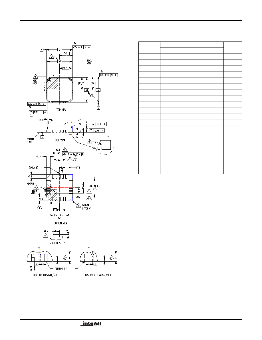
Quad Flat No-Lead Plastic Package (QFN)
Micro Lead Frame Plastic Package (MLFP)
L32.7x7A
32 LEAD QUAD FLAT NO-LEAD PLASTIC PACKAGE
(COMPLIANT TO JEDEC MO-220VKKC ISSUE C)
SYMBOL
MILLIMETERS
NOTES
MIN
NOMINAL
MAX
A
0.80
0.90
1.00
-
A1
-
-
0.05
-
A2
-
-
1.00
9
A3
0.20 REF
9
b
0.23
0.28
0.38
5, 8
D
7.00 BSC
-
D1
6.75 BSC
9
D2
4.95
5.10
5.25
7, 8
E
7.00 BSC
-
E1
6.75 BSC
9
E2
4.95
5.10
5.25
7, 8
e
0.65 BSC
-
k
0.25
-
-
-
L
0.35
0.60
0.75
8
L1 -
-
0.15
10
N
32
2
Nd
8
3
Ne
8
3
P
-
-
0.60
9
-
-
12
9
Rev. 1 10/02
NOTES:
1. Dimensioning and tolerancing conform to ASME Y14.5-1994.
2. N is the number of terminals.
3. Nd and Ne refer to the number of terminals on each D and E.
4. All dimensions are in millimeters. Angles are in degrees.
5. Dimension b applies to the metallized terminal and is measured
between 0.15mm and 0.30mm from the terminal tip.
6. The configuration of the pin #1 identifier is optional, but must be
located within the zone indicated. The pin #1 identifier may be
either a mold or mark feature.
7. Dimensions D2 and E2 are for the exposed pads which provide
improved electrical and thermal performance.
8. Nominal dimensions are provided to assist with PCB Land Pattern
Design efforts, see Intersil Technical Brief TB389.
9. Features and dimensions A2, A3, D1, E1, P &
are present when
Anvil singulation method is used and not present for saw
singulation.
10. Depending on the method of lead termination at the edge of the
package, a maximum 0.15mm pull back (L1) maybe present. L
minus L1 to be equal to or greater than 0.3mm.