1
TM
June 1998
HD-4702/883
CMOS Programmable Bit Rate Generator
Features
∑ This Circuit is Processed in Accordance to MIL-STD-883
and is Fully Conformant Under the Provisions of
Paragraph 1. 2. 1.
∑ HD-4702/883 Provides 13 Commonly Used Bit Rates
∑ Uses a 2.4576MHz Crystal/Input for Standard
Frequency Output (16 Times Bit Rate)
∑ Low Power Dissipation
∑ Conforms to ElA RS-404
∑ One HD-4702/883 Controls up to Eight Transmission
Channels
∑ Initialization Circuit Facilitates Diagnostic Fault
Isolation
∑ On-Chip Input Pull-Up Circuit
Description
The HD-4702/883 Bit Rate Generator provides the
necessary clock signals for digital data transmission sys-
tems, such as a UART. It generates 13 commonly used bit
rates using an on-chip crystal oscillator or an external input.
For conventional operation generating 16 output clock
pulses per bit period, the input clock frequency must be
2.4576MHz (i.e., 9600 Baud x 16 x 16, since there is an
internal
˜
16 prescaler). A lower input frequency will result in
a proportionally lower output frequency.
The HD-4702/883 can provide multi-channel operation with
a minimum of external logic by having the clock frequency
C
O
and the
˜
8 prescaler outputs Q
0
, Q
1
, Q
2
available
externally. All signals have a 50% duty cycle except 1800
Baud, which has less than 0.39% distortion.
The four rate select inputs (S
0
-S
3
) select which bit rate is at
the output (Z). See Truth Table for Rate Select Inputs for
select code and output bit rate. Two of the 16 select codes
for the HD-4702/883 do not select an internally generated
frequency, but select an input into which the user can feed
either a different frequency, or a static level (High or Low) to
generate "ZERO BAUD".
The bit rates most commonly used in modern data terminals
(110,150, 300,1200, 2400 Baud) require that no more than
one input be grounded for the HD-4702/883, which is easily
achieved with a single 5-position switch.
The HD-4702/883 has an initialization circuit which
generates a master reset for the scan counter. This signal is
derived from a digital differentiator that senses the first high
level on the C
P
input after the E
CP
input goes low. When
E
CP
is high, selecting the crystal input, C
P
must be low. A
high level on C
P
would apply a continuous reset. See Clock
Modes and Initialization below.
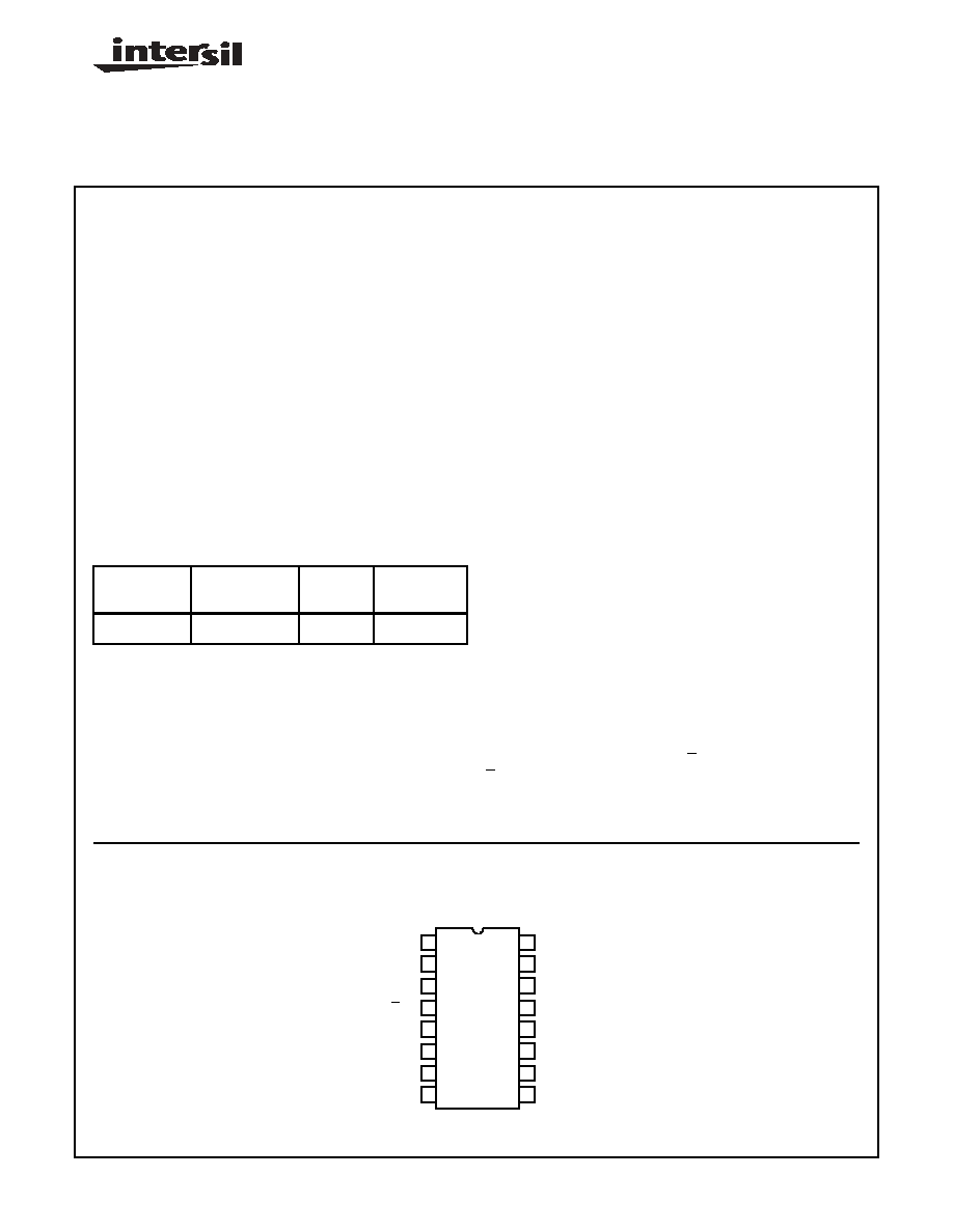
Pinout
HD-4702/883 (CERDIP)
TOP VIEW
Ordering Information
PART
NUMBER
TEMPERATURE
RANGE (
o
C)
PACKAGE
PKG. NO.
HD1-4702/883
-55 to 125
CERDIP
F16.3
14
15
16
9
13
12
11
10
1
2
3
4
5
7
6
8
Q
0
Q
1
Q
2
E
CP
C
P
O
X
GND
I
X
V
CC
I
M
S
0
S
1
S
2
Z
S
3
C
O
FN2955.2
CAUTION: These devices are sensitive to electrostatic discharge; follow proper IC Handling Procedures.
1-888-INTERSIL or 321-724-7143
|
Intersil (and design) is a trademark of Intersil Americas Inc.
Copyright © Intersil Americas Inc. 2002. All Rights Reserved

2
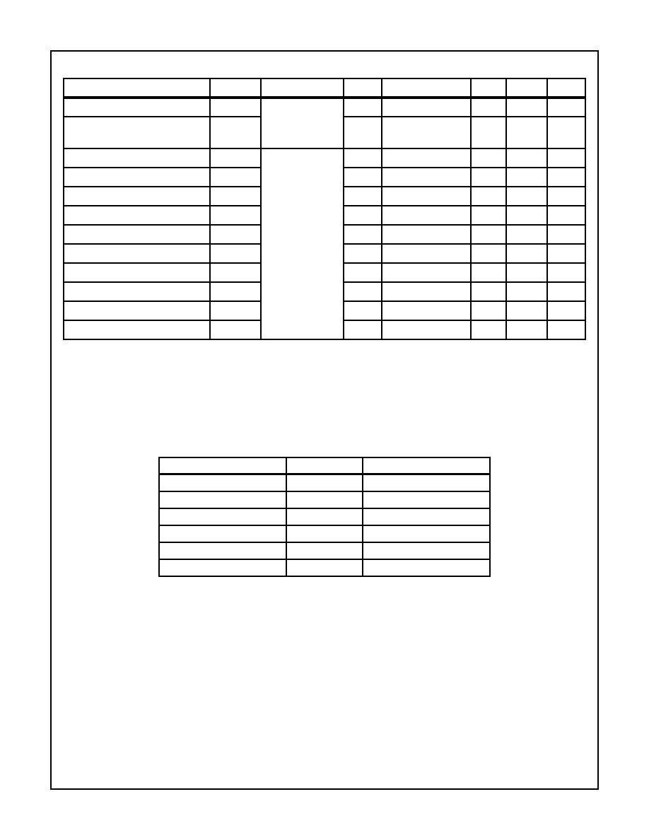
Truth Table
TRUTH TABLE FOR RATE SELECT INPUTS
(Using 2.4576MHz Crystal)
S
3
S
2
S
1
S
0
OUTPUT RATE (Z)
L
L
L
L
MUX Input (l
M
)
L
L
L
H
MUX Input (l
M
)
L
L
H
L
50 Baud
L
L
H
H
75 Baud
L
H
L
L
134.5 Baud
L
H
L
H
200 Baud
L
H
H
L
600 Baud
L
H
H
H
2400 Baud
H
L
L
L
9600 Baud
H
L
L
H
4800 Baud
H
L
H
L
1800 Baud
H
L
H
H
1200 Baud
H
H
L
L
2400 Baud
H
H
L
H
300 Baud
H
H
H
L
150 Baud
H
H
H
H
110 Baud
NOTE:
1. 19200 Baud by connecting Q
2
to I
M
.
CLOCK MODES AND INITIALIZATION
I
X
E
CP
C
P
OPERATION
H
L
Clocked from I
X
X
L
Clocked from C
P
X
H
H
Continuous Reset
X
L
Reset During First C
P
= High Time
NOTE:
2. Actual output frequency is 16 times the indicated output
rate, assuming a clock frequency of 2.4576MHz.
H
= HIGH Level
L
= LOW Level
X
= Don't Care
= Clock Pulse
= First HIGH Level Clock Pulse after E
CP
goes LOW
HD-4702/883

3
Absolute Maximum Ratings
Thermal Information
Supply Voltage . . . . . . . . . . . . . . . . . . . . . . . . . . . . . . . . . . . . . +8.0V
Input, Output or I/O Voltage . . . . . . . . . . . GND -0.5V to V
CC
+0.5V
ESD Classification . . . . . . . . . . . . . . . . . . . . . . . . . . . . . . . . Class 1
Typical Derating Factor . . . . . . . . . . . 1mA/MHz Increase in ICCOP
Operating Conditions
Operating Voltage Range . . . . . . . . . . . . . . . . . . . . . +4.5V to +5.5V
Operating Temperature Range. . . . . . . . . . . . . . . . . -55
o
C to 125
o
C
Thermal Resistance, (Typical, Note 3)
JA
(
o
C/W)
JC
(
o
C/W)
CERDIP Package . . . . . . . . . . . . . .
78
23
Maximum Storage Temperature Range . . . . . . . . . . -65
o
C to 150
o
C
Maximum Junction Temperature. . . . . . . . . . . . . . . . . . . . . . . 175
o
C
Maximum Lead Temperature (Soldering, 10s) . . . . . . . . . . . . 300
o
C
Die Characteristics
Gate Count . . . . . . . . . . . . . . . . . . . . . . . . . . . . . . . . . . . . 720 Gates
CAUTION: Stresses above those listed in "Absolute Maximum Ratings" may cause permanent damage to the device. This is a stress only rating and operation
of the device at these or any other conditions above those indicated in the operational sections of this specification is not implied.
NOTE:
3.
JA
is measured with the component mounted on an evaluation PC board in free air.
TABLE 1. DC ELECTRICAL PERFORMANCE SPECIFICATIONS
Device Guaranteed and 100% Tested
DC PARAMETER
SYMBOL
CONDITIONS
GROUP A
SUB-
GROUPS
TEMPERATURE
(
o
C)
MIN
MAX
UNITS
Input High Voltage
V
IH
V
CC
= 4.5V
1, 2, 3
-55
TA
125
V
CC
70%
-
V
Input Low Voltage
V
IL
V
CC
= 4.5V
1, 2, 3
-55
TA
125
-
V
CC
30%
V
Output High Voltage
V
OH1
I
OH
-1
µ
A, V
CC
= 4.5V,
(Note 4)
1, 2, 3
-55
TA
125
V
CC
-0.1
-
V
Output Low Voltage
V
OL1
I
OL
+1
µ
A, V
CC
= 4 5V,
(Note 4)
1, 2, 3
-55
TA
125
-
0.1
V
Input High Current
I
IH
V
IN
= V
CC
. All Other Pins = 0V,
V
CC
= 5.5V
1, 2, 3
-55
TA
125
-1
+1
µ
A
Input Low Current
(IX Input)
I
ILX
V
IN
= 0V, All Other Pins = V
CC
,
V
CC
= 5.5V
1, 2, 3
-55
TA
125
-1
+1
µ
A
Input Low Current
(All Other Inputs)
I
lL
V
IN
= 0V All Other Pins = V
CC
,
V
CC
= 5.5V (Note 5)
1, 2, 3
-55
TA
125
-
-100
µ
A
Output High Current
(OX)
I
OHX
V
OUT
= V
CC
-0.5, V
CC
= 4.5V
Input at 0V or V
CC
per Logic
Function or Truth Table
1, 2, 3
-55
TA
125
-0.1
-
mA
Output High Current
(All Other Outputs)
I
OH1
V
OUT
= 2.5V, V
CC
= 4.5V
Input at 0V or V
CC
per Logic
Function or Truth Table
1, 2, 3
-55
TA
125
-1.0
-
mA
Output High Current
(All Other Outputs)
I
OH2
V
OUT
= V
CC
-0.5, V
CC
= 4.5V
Input at 0V or V
CC
per Logic
Function or Truth Table
1, 2, 3
-55
TA
125
-0.3
-
mA
Output Low Current
(OX)
I
OLX
V
OUT
= 0.4V, V
CC
= 4.5V
Input at 0V or V
CC
per Logic
Function or Truth Table
1, 2, 3
-55
TA
125
0.1
-
mA
Output Low Current
(All Other Outputs)
I
OL
V
OUT
= 0.4V, V
CC
= 4.5V
Input at 0V or V
CC
per Logic
Function or Truth Table
1, 2, 3
-55
TA
125
1.6
-
mA
HD-4702/883

4
Supply Current
(Static)
I
CC
ECP = V
CC
, CP = 0V,
V
CC
= 5.5V
All Other Inputs = GND,
(Note 5)
1, 2, 3
-55
TA
125
-
1500
µ
A
ECP = V
CC
, CP = 0V,
V
CC
= 5.5V
All Other Inputs = V
CC
(Note 5)
1, 2, 3
-55
TA
125
-
1000
µ
A
NOTES:
4. Interchanging of force and sense conditions is permitted.
5. Input Current and Quiescent Power Supply Current are relatively higher for this device because of active pull-up circuits on all inputs
except I
X
.
TABLE 2. AC ELECTRICAL PERFORMANCE SPECIFICATIONS
Device Guaranteed and 100% Tested.
AC PARAMETER
SYMBOL
CONDITIONS
GROUP A
SUBGROUPS
TEMPERATURE
(
o
C)
MIN
MAX
UNITS
Propagation Delay, I
X
to C
O
t
PLH
V
CC
= 4.5V
C
L
7pF on OX
C
L
= 50pF
(Note 6)
9, 10, 11
-55
T
A
125
-
350
ns
Propagation Delay, I
X
to C
O
t
PHL
9, 10, 11
-55
T
A
125
-
275
ns
Propagation Delay, C
P
to C
O
t
PLH
9, 10, 11
-55
T
A
125
-
260
ns
Propagation Delay, C
P
to C
O
t
PHL
9, 10, 11
-55
T
A
125
-
220
ns
Propagation Delay, C
O
to Qn
t
PLH
9, 10, 11
-55
T
A
125
-
(Note 7)
ns
Propagation Delay, C
O
to Q
n
t
PHL
9, 10, 11
-55
T
A
125
-
(Note 7)
ns
Propagation Delay, C
O
to Z
t
PLH
9, 10, 11
-55
T
A
125
-
85
ns
Propagation Delay, C
O
to Z
t
PHL
9, 10, 11
-55
T
A
125
-
75
ns
Output Transition Time (Except O
X
)
t
TLH
9, 10, 11
-55
T
A
125
160
ns
Output Transition Time (Except O
X
)
t
THL
9, 10, 11
-55
T
A
125
-
75
ns
Set-UpTime Select to C
O
t
S
9, 10, 11
-55
T
A
125
350
-
ns
Hold Time, Select to C
O
t
H
9, 10, 11
-55
T
A
125
0
-
ns
Set-UpTime, I
M
to C
O
t
S
9, 10, 11
-55
T
A
125
350
-
ns
Hold Time, I
M
to C
O
t
H
9, 10, 11
-55
T
A
125
0
-
ns
Minimum Clock Pulse Width, Low
(Notes 8, 9)
t
WCP(L)
9, 10, 11
-55
T
A
125
120
ns
Minimum Clock Pulse Width, High
(Notes 8, 9)
t
WCP(H)
9, 10, 11
-55
T
A
125
120
-
ns
Minimum I
X
Pulse Width, Low (Note 9)
t
WCP(L)
9, 10, 11
-55
T
A
125
160
-
ns
Minimum I
X
Pulse Width, High (Note 9)
t
WCP(H)
9, 10, 11
-55
T
A
125
160
-
ns
NOTES:
6. Propagation Delays (t
PLH
and t
PHL
) and Output Transition Times (t
TLH
and t
THL
) will change with Output Load Capacitance (C
L
).
Set-Up Times (t
S
), Hold Times (t
H
), and Minimum Pulse Widths (t
W
) do not vary with load capacitance.
7. For multichannel operation, Propagation Delay (C
O
to Qn), plus Set-Up Time, Select to C
O
, is guaranteed to be
367ns.
8. The first High Level Clock Pulse alter E
CP
goes Low must be at least 350ns long to guarantee reset of all Counters.
9. It is recommended that input rise and fall times to the clock inputs (C
P
, I
X
) be less than 15ns.
TABLE 1. DC ELECTRICAL PERFORMANCE SPECIFICATIONS (Continued)
Device Guaranteed and 100% Tested
DC PARAMETER
SYMBOL
CONDITIONS
GROUP A
SUB-
GROUPS
TEMPERATURE
(
o
C)
MIN
MAX
UNITS
HD-4702/883
5
TABLE 3. ELECTRICAL PERFORMANCE SPECIFICATIONS
AC PARAMETER
SYMBOL
CONDITIONS
NOTES TEMPERATURE (
o
C)
MIN
MAX
UNITS
Input Capacitance
C
IN
All Measurements
are referenced to
device ground,
f = 1MHz.
10
T
A
= 25
-
7.0
pF
Output Capacitance
C
O
10
T
A
= 25
-
15.0
pF
Propagation Delay I
X
to C
O
t
PLH
V
CC
= 4.5V
C
L
7pF on O
X
C
L
= 15pF
10, 12
-55
T
A
125
-
300
ns
Propagation Delay I
X
to C
O
t
PHL
10, 12
-55
T
A
125
-
250
ns
Propagation Delay C
P
to C
O
t
PLH
10, 12
-55
T
A
125
-
215
ns
Propagation Delay C
P
to C
O
t
PHL
10, 12
-55
T
A
125
-
195
ns
Propagation Delay C
O
to Qn
t
PLH
10, 12
-55
T
A
125
-
(Note 11)
ns
Propagation Delay C
O
to Qn
t
PHL
10, 12
-55
T
A
125
-
(Note 11)
ns
Propagation Delay C
O
to Z
t
PLH
10, 12
-55
T
A
125
-
75
ns
Propagation Delay C
O
to Z
t
PHL
10, 12
-55
T
A
125
-
65
ns
Output Transition Time (Except O
X
)
t
TLH
10, 12
-55
T
A
125
-
80
ns
Output Transition Time (Except O
X
)
t
THL
10, 12
-55
T
A
125
-
40
ns
NOTES:
10. The parameters listed in Table 3 are controlled via design or process parameters and are not directly tested. These parameters are
characterized upon initial design and after major process and/or design changes.
11. For multichannel operation, Propagation Delay (C
O
to Qn) plus Set-Up Time, Select to C
O
, is guaranteed to be
367ns.
12. Propagation Delays (t
PLH
and t
PHL
) and Output Transition Times (t
TLH
and t
THL
) will change with Output Load Capacitance (C
L
).
Set-Up Times (t
S
), Hold Times (t
H
), and Minimum Pulse Widths (t
W
) do not vary with load capacitance.
TABLE 4. APPLICABLE SUBGROUPS
CONFORMANCE GROUPS
METHOD
SUBGROUPS
Initial Test
100%/5004
-
Interim Test
100%/5004
1, 7, 9
PDA
100%
1
Final Test
100%
2, 3, 8A, 8B, 10, 11
Group A
-
1, 2, 3, 7, 8A, 8B, 9, 10, 11
Groups C and D
Samples/5005
1, 7, 9
HD-4702/883