 | –≠–ª–µ–∫—Ç—Ä–æ–Ω–Ω—ã–π –∫–æ–º–ø–æ–Ω–µ–Ω—Ç: HFA1100IB | –°–∫–∞—á–∞—Ç—å:  PDF PDF  ZIP ZIP |
1
CAUTION: These devices are sensitive to electrostatic discharge; follow proper IC Handling Procedures.
http://www.intersil.com or 407-727-9207 | Copyright © Intersil Corporation 1999
HFA1100, HFA1120
850MHz, Low Distortion Current Feedback
Operational Amplifiers
The HFA1100, 1120 are a family of high-speed, wideband,
fast settling current feedback amplifiers built with Intersil's
proprietary complementary bipolar UHF-1 process. Both
amplifiers operate with single supply voltages as low as 4.5V
(see Application Information section).
The HFA1100 is a basic op amp with uncommitted pins 1, 5,
and 8. The HFA1120 includes inverting input bias current
adjust pins (pins 1 and 5) for adjusting the output offset
voltage.
These devices offer a significant performance improvement
over the AD811, AD9617/18, the CLC400-409, and the
EL2070, EL2073, EL2030.
For Military grade product refer to the HFA1100/883,
HFA1120/883 data sheet.
The Op Amps with Fastest Edges
Features
∑ Low Distortion (30MHz, HD2). . . . . . . . . . . . . . . . . -56dBc
∑ -3dB Bandwidth . . . . . . . . . . . . . . . . . . . . . . . . . . 850MHz
∑ Very Fast Slew Rate . . . . . . . . . . . . . . . . . . . . . . 2300V/
µ
s
∑ Fast Settling Time (0.1%) . . . . . . . . . . . . . . . . . . . . . 11ns
∑ Excellent Gain Flatness
- (100MHz) . . . . . . . . . . . . . . . . . . . . . . . . . . . . .
±
0.14dB
- (50MHz) . . . . . . . . . . . . . . . . . . . . . . . . . . . . . .
±
0.04dB
∑ High Output Current . . . . . . . . . . . . . . . . . . . . . . . . . 60mA
∑ Overdrive Recovery . . . . . . . . . . . . . . . . . . . . . . . . <10ns
∑ Operates with 5V Single Supply (See AN9745)
Applications
∑ Video Switching and Routing
∑ Pulse and Video Amplifiers
∑ RF/IF Signal Processing
∑ Flash A/D Driver
∑ Medical Imaging Systems
∑ Related Literature
- AN9420, Current Feedback Theory
- AN9202, HFA11XX Evaluation Fixture
- AN9745, Single 5V Supply Operation
Pinouts
HFA1100
(PDIP, SOIC)
TOP VIEW
HFA1120
(SOIC)
TOP VIEW
Ordering Information
PART NUMBER
(BRAND)
TEMP.
RANGE (
o
C)
PACKAGE
PKG. NO.
HFA1100IP
-40 to 85
8 Ld PDIP
E8.3
HFA1100IB
(H1100I)
-40 to 85
8 Ld SOIC
M8.15
HFA1120IB
(H1120I)
-40 to 85
8 Ld SOIC
M8.15
HFA11XXEVAL
DIP Evaluation Board for High-Speed Op Amps
INPUT
220MHz
SIGNAL
OUTPUT
(A
V
= 2)
HFA1130
OP AMP
0ns
25ns
NC
-IN
+IN
V-
1
2
3
4
8
7
6
5
NC
V+
OUT
NC
-
+
BAL
-IN
+IN
V-
1
2
3
4
8
7
6
5
NC
V+
OUT
BAL
-
+
Data Sheet
May 1999
File Number
2945.7
2
Absolute Maximum Ratings
T
A
= 25
o
C
Thermal Information
Voltage Between V+ and V- . . . . . . . . . . . . . . . . . . . . . . . . . . . . 12V
Input Voltage . . . . . . . . . . . . . . . . . . . . . . . . . . . . . . . . . . . V
SUPPLY
Differential Input Voltage . . . . . . . . . . . . . . . . . . . . . . . . . . . . . . . 5V
Output Current (50% Duty Cycle) . . . . . . . . . . . . . . . . . . . . . . 60mA
Operating Conditions
Temperature Range . . . . . . . . . . . . . . . . . . . . . . . . . . -40
o
C to 85
o
C
Thermal Resistance (Typical, Note 1)
JA
(
o
C/W)
JC
(
o
C/W)
PDIP Package . . . . . . . . . . . . . . . . . . .
130
N/A
SOIC Package . . . . . . . . . . . . . . . . . . .
170
N/A
Maximum Junction Temperature (Plastic Package) . . . . . . . . .150
o
C
Maximum Storage Temperature Range . . . . . . . . . . -65
o
C to 150
o
C
Maximum Lead Temperature (Soldering 10s) . . . . . . . . . . . . 300
o
C
(SOIC - Lead Tips Only)
CAUTION: Stresses above those listed in "Absolute Maximum Ratings" may cause permanent damage to the device. This is a stress only rating and operation of the
device at these or any other conditions above those indicated in the operational sections of this specification is not implied.
NOTE:
1.
JA
is measured with the component mounted on an evaluation PC board in free air.
Electrical Specifications
V
SUPPLY
=
±
5V, A
V
= +1, R
F
= 510
, R
L
= 100
, Unless Otherwise Specified
PARAMETER
TEST
CONDITIONS
(NOTE 2)
TEST
LEVEL
TEMP.
(
o
C)
MIN
TYP
MAX
UNITS
INPUT CHARACTERISTICS
Input Offset Voltage (Note 3)
A
25
-
2
6
mV
A
Full
-
-
10
mV
Input Offset Voltage Drift
C
Full
-
10
-
µ
V/
o
C
V
IO
CMRR
V
CM
=
±
2V
A
25
40
46
-
dB
A
Full
38
-
-
dB
V
IO
PSRR
V
S
=
±
1.25V
A
25
45
50
-
dB
A
Full
42
-
-
dB
Non-Inverting Input Bias Current
(Note 3)
+IN = 0V
A
25
-
25
40
µ
A
A
Full
-
-
65
µ
A
+I
BIAS
Drift
C
Full
-
40
-
nA/
o
C
+I
BIAS
CMS
V
CM
=
±
2V
A
25
-
20
40
µ
A/V
A
Full
-
-
50
µ
A/V
Inverting Input Bias Current (Note 3)
-IN = 0V
A
25
-
12
50
µ
A
A
Full
-
-
60
µ
A
-I
BIAS
Drift
C
Full
-
40
-
nA/
o
C
-I
BIAS
CMS
V
CM
=
±
2V
A
25
-
1
7
µ
A/V
A
Full
-
-
10
µ
A/V
-I
BIAS
PSS
V
S
=
±
1.25V
A
25
-
6
15
µ
A/V
A
Full
-
-
27
µ
A/V
-I
BIAS
Adj. Range (HFA1120)
A
25
±
100
±
200
-
µ
A
Non-Inverting Input Resistance
A
25
25
50
-
k
Inverting Input Resistance
C
25
-
20
30
Input Capacitance (Either Input)
B
25
-
2
-
pF
Input Common Mode Range
C
Full
±
2.5
±
3.0
-
V
Input Noise Voltage (Note 3)
100kHz
B
25
-
4
-
nV/
Hz
+Input Noise Current (Note 3)
100kHz
B
25
-
18
-
pA/
Hz
-Input Noise Current (Note 3)
100kHz
B
25
-
21
-
pA/
Hz
HFA1100, HFA1120
3
TRANSFER CHARACTERISTICS
A
V
= +2, Unless Otherwise Specified
Open Loop Transimpedance (Note 3)
B
25
-
300
-
k
-3dB Bandwidth (Note 3)
V
OUT
= 0.2V
P-P
,
A
V
= +1
B
25
530
850
-
MHz
-3dB Bandwidth
V
OUT
= 0.2V
P-P
,
A
V
= +2, R
F
= 360
B
25
-
670
-
MHz
Full Power Bandwidth
V
OUT
= 4V
P-P
,
A
V
= -1
B
25
-
300
-
MHz
Gain Flatness (Note 3)
To 100MHz
B
25
-
±
0.14
-
dB
Gain Flatness
To 50MHz
B
25
-
±
0.04
-
dB
Gain Flatness
To 30MHz
B
25
-
±
0.01
-
dB
Linear Phase Deviation (Note 3)
DC to 100MHz
B
25
-
0.6
-
Degrees
Differential Gain
NTSC, R
L
= 75
B
25
-
0.03
-
%
Differential Phase
NTSC, R
L
= 75
B
25
-
0.05
-
Degrees
Minimum Stable Gain
A
Full
1
-
-
V/V
OUTPUT CHARACTERISTICS
A
V
= +2, Unless Otherwise Specified
Output Voltage (Note 3)
A
V
= -1
A
25
±
3.0
±
3.3
-
V
A
Full
±
2.5
±
3.0
-
V
Output Current
R
L
= 50
, A
V
= -1
A
25, 85
50
60
-
mA
A
-40
35
50
-
mA
DC Closed Loop Output Impedance
(Note 3)
B
25
-
0.07
-
2nd Harmonic Distortion (Note 3)
30MHz, V
OUT
= 2V
P-P
B
25
-
-56
-
dBc
3rd Harmonic Distortion (Note 3)
30MHz, V
OUT
= 2V
P-P
B
25
-
-80
-
dBc
3rd Order Intercept (Note 3)
100MHz
B
25
20
30
-
dBm
1dB Compression
100MHz
B
25
15
20
-
dBm
TRANSIENT RESPONSE
A
V
= +2, Unless Otherwise Specified
Rise Time
V
OUT
= 2.0V Step
B
25
-
900
-
ps
Overshoot (Note 3)
V
OUT
= 2.0V Step
B
25
-
10
-
%
Slew Rate
A
V
= +1, V
OUT
= 5V
P-P
B
25
-
1400
-
V/
µ
s
Slew Rate
A
V
= +2, V
OUT
= 5V
P-P
B
25
1850
2300
-
V/
µ
s
0.1% Settling (Note 3)
V
OUT
= 2V to 0V
B
25
-
11
-
ns
0.2% Settling (Note 3)
V
OUT
= 2V to 0V
B
25
-
7
-
ns
Overdrive Recovery Time
2X Overdrive
B
25
-
7.5
10
ns
POWER SUPPLY CHARACTERISTICS
Supply Voltage Range
B
Full
±
4.5
-
±
5.5
V
Supply Current (Note 3)
A
25
-
21
26
mA
A
Full
-
-
33
mA
NOTES:
2. Test Level: A. Production Tested; B. Typical or Guaranteed Limit Based on Characterization; C. Design Typical for Information Only.
3. See Typical Performance Curves for more information.
Electrical Specifications
V
SUPPLY
=
±
5V, A
V
= +1, R
F
= 510
, R
L
= 100
, Unless Otherwise Specified (Continued)
PARAMETER
TEST
CONDITIONS
(NOTE 2)
TEST
LEVEL
TEMP.
(
o
C)
MIN
TYP
MAX
UNITS
HFA1100, HFA1120

4
Application Information
Optimum Feedback Resistor (R
F
)
The enclosed plots of inverting and non-inverting frequency
response detail the performance of the HFA1100/1120 in
various gains. Although the bandwidth dependency on A
CL
isn't as severe as that of a voltage feedback amplifier, there is
an appreciable decrease in bandwidth at higher gains. This
decrease can be minimized by taking advantage of the
current feedback amplifier's unique relationship between
bandwidth and R
F
. All current feedback amplifiers require a
feedback resistor, even for unity gain applications, and the R
F
,
in conjunction with the internal compensation capacitor, sets
the dominant pole of the frequency response. Thus, the
amplifier's bandwidth is inversely proportional to R
F
. The
HFA1100, 1120 designs are optimized for a 510
R
F
, at a
gain of +1. Decreasing R
F
in a unity gain application
decreases stability, resulting in excessive peaking and
overshoot (Note: Capacitive feedback causes the same
problems due to the feedback impedance decrease at higher
frequencies). At higher gains the amplifier is more stable, so
R
F
can be decreased in a trade-off of stability for bandwidth.
The table below lists recommended R
F
values for various
gains, and the expected bandwidth.
Offset Adjustment
The HFA1120 allows for adjustment of the inverting input
bias current to null the output offset voltage. -I
BIAS
flows
through R
F
, so any change in bias current forces a
corresponding change in output voltage. The amount of
adjustment is a function of R
F
. With R
F
= 510
, the typical
adjust range is
±
100mV. For offset adjustment connect a
10k
potentiometer between pins 1 and 5 with the wiper
connected to V-.
5V Single Supply Operation
These amplifiers will operate at single supply voltages down
to 4.5V. The table below details the amplifier's performance
with a single 5V supply. The dramatic supply current
reduction at this operating condition (refer also to Figure 23)
makes these op amps even better choices for low power 5V
systems. Refer to Application Note AN9745 for further
information.
Use of Die in Hybrid Applications
These amplifiers are designed with compensation to negate
the package parasitics that typically lead to instabilities. As a
result, the use of die in hybrid applications results in
overcompensated performance due to lower parasitic
capacitances. Reducing R
F
below the recommended values
for packaged units will solve the problem. For A
V
= +2 the
recommended starting point is 300
, while unity gain
applications should try 400
.
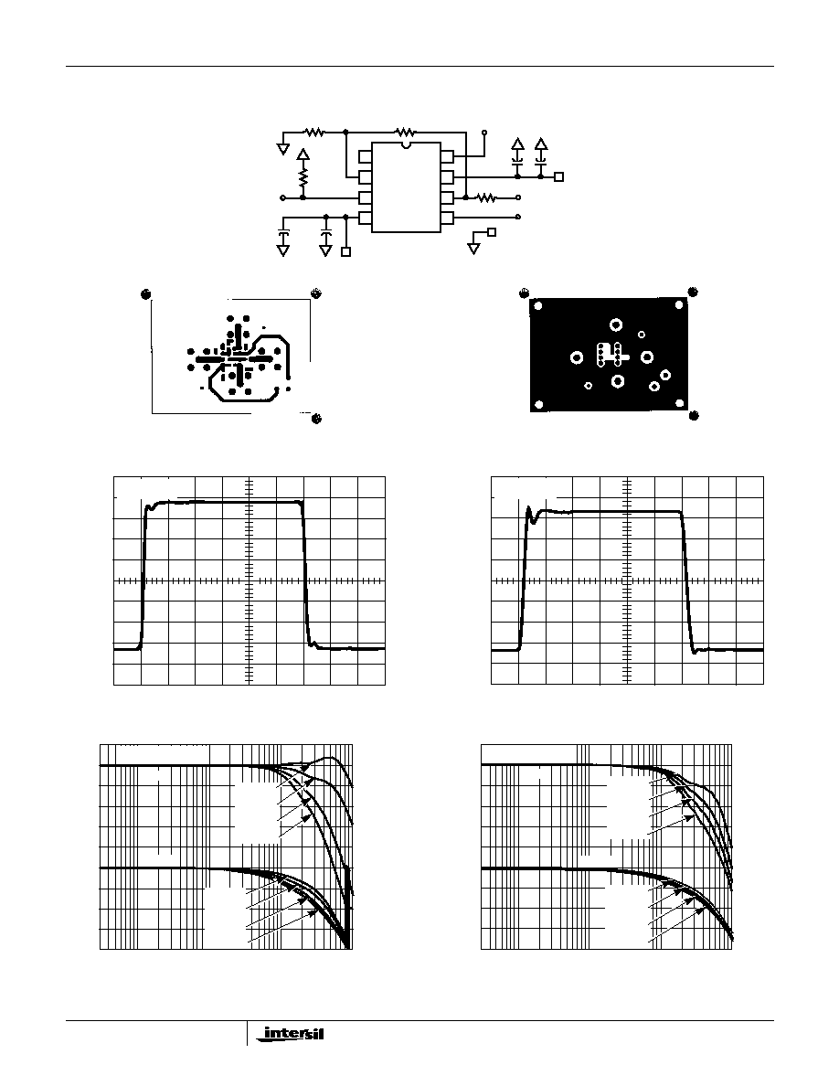
PC Board Layout
The frequency performance of these amplifiers depends a
great deal on the amount of care taken in designing the PC
board. The use of low inductance components such as
chip resistors and chip capacitors is strongly
recommended, while a solid ground plane is a must!
Attention should be given to decoupling the power supplies.
A large value (10
µ
F) tantalum in parallel with a small value
chip (0.1
µ
F) capacitor works well in most cases.
Terminated microstrip signal lines are recommended at the
input and output of the device. Output capacitance, such as
that resulting from an improperly terminated transmission
line will degrade the frequency response of the amplifier and
may cause oscillations. In most cases, the oscillation can be
avoided by placing a resistor in series with the output.
Care must also be taken to minimize the capacitance to ground
seen by the amplifier's inverting input. The larger this
capacitance, the worse the gain peaking, resulting in pulse
overshoot and possible instability. To this end, it is
recommended that the ground plane be removed under traces
connected to pin 2, and connections to pin 2 should be kept as
short as possible.
An example of a good high frequency layout is the
Evaluation Board shown below.
Evaluation Board
An evaluation board is available for the HFA1100 (Part
Number HFA11XXEVAL). Please contact your local sales
office for information.
A
CL
R
F
(
)
BW (MHz)
+1
510
850
-1
430
580
+2
360
670
+5
150
520
+10
180
240
+19
270
125
PARAMETER
TYP
Input Common Mode Range
1V to 4V
-3dB BW (A
V
= +2)
267MHz
Gain Flatness (to 50MHz, A
V
= +2)
0.05dB
Output Voltage (A
V
= -1)
1.3V to 3.8V
Slew Rate (A
V
= +2)
475V/
µ
s
0.1% Settling Time
17ns
Supply Current
5.5mA
HFA1100, HFA1120
5
The layout and schematic of the board are shown below:
TOP LAYOUT
BOTTOM LAYOUT
1
2
3
4
8
7
6
5
+5V
10
µ
F
0.1
µ
F
V
H
50
GND
GND
500
500
-5V
0.1
µ
F
10
µ
F
50
IN
OUT
V
L
V
H
+IN
V
L
V+
GND
1
V-
OUT
Typical Performance Curves
V
SUPPLY
=
±
5V, R
F
= 510
, T
A
= 25
o
C, R
L
= 100
,
Unless Otherwise Specified
FIGURE 1. SMALL SIGNAL PULSE
FIGURE 2. LARGE SIGNAL PULSE
FIGURE 3. NON-INVERTING FREQUENCY RESPONSE
FIGURE 4. INVERTING FREQUENCY RESPONSE
120
TIME (5ns/DIV.)
90
60
30
0
-30
-60
-90
-120
OUTPUT V
O
L
T
A
GE (mV)
A
V
= +2
OUTPUT V
O
L
T
A
GE (V)
1.2
0.9
0.6
0.3
0
-0.3
-0.6
-0.9
-1.2
A
V
= +2
TIME (5ns/DIV.)
FREQUENCY (MHz)
0
-3
-6
-9
-12
NORMALIZED GAIN (dB)
0.3
1
10
100
1K
0
-90
-180
-270
-360
PHASE
GAIN
A
V
= +1
A
V
= +1
A
V
= +11
A
V
= +2
A
V
= +6
A
V
= +11
A
V
= +2
A
V
= +6
PHASE (DEGREES)
V
OUT
= 200mV
P-P
FREQUENCY (MHz)
PHASE
GAIN
0
-3
-6
-9
-12
NORMALIZED GAIN (dB)
0.3
1
10
100
1K
180
90
0
-90
-180
A
V
= -1
A
V
= -1
A
V
= -20
A
V
= -5
A
V
= -10
A
V
= -20
A
V
= -5
A
V
= -10
PHASE (DEGREES)
V
OUT
= 200mV
P-P
HFA1100, HFA1120