 | –≠–ª–µ–∫—Ç—Ä–æ–Ω–Ω—ã–π –∫–æ–º–ø–æ–Ω–µ–Ω—Ç: HFA1130IB | –°–∫–∞—á–∞—Ç—å:  PDF PDF  ZIP ZIP |

1
CAUTION: These devices are sensitive to electrostatic discharge; follow proper IC Handling Procedures.
http://www.intersil.com or 407-727-9207 | Copyright © Intersil Corporation 1999
HFA1130
850MHz, Output Limiting, Low Distortion
Current Feedback Operational Amplifier
The HFA1130 is a high speed wideband current feedback
amplifier featuring programmable output limits. Built with
Intersil's proprietary complementary bipolar UHF-1 process,
it is the fastest monolithic amplifier available from any
semiconductor manufacturer.
This amplifier is the ideal choice for high frequency
applications requiring output limiting, especially those needing
ultra fast overdrive recovery times. The output limiting function
allows the designer to set the maximum positive and negative
output levels, thereby protecting later stages from damage or
input saturation. The sub-nanosecond overdrive recovery time
quickly returns the amplifier to linear operation, following an
overdrive condition.
The HFA1130 offers significant performance improvements
over the CLC500/501/502.
A variety of packages and temperature grades are available.
See the ordering information below for details. For /883
product refer to the HFA1130/883 datasheet.
The Op Amps With Fastest Edges
Features
∑ User Programmable Output Voltage Limits
∑ Low Distortion (30MHz, HD2). . . . . . . . . . . . . . . . . -56dBc
∑ -3dB Bandwidth . . . . . . . . . . . . . . . . . . . . . . . . . . 850MHz
∑ Very Fast Slew Rate . . . . . . . . . . . . . . . . . . . . . . 2300V/
µ
s
∑ Fast Settling Time (0.1%) . . . . . . . . . . . . . . . . . . . . . 11ns
∑ Excellent Gain Flatness
- (100MHz) . . . . . . . . . . . . . . . . . . . . . . . . . . . . . . 0.14dB
- (50MHz) . . . . . . . . . . . . . . . . . . . . . . . . . . . . . . . 0.04dB
- (30MHz) . . . . . . . . . . . . . . . . . . . . . . . . . . . . . . . 0.01dB
∑ High Output Current . . . . . . . . . . . . . . . . . . . . . . . . . 60mA
∑ Overdrive Recovery . . . . . . . . . . . . . . . . . . . . . . . . . <1ns
Applications
∑ Residue Amplifier
∑ Video Switching and Routing
∑ Pulse and Video Amplifiers
∑ Wideband Amplifiers
∑ RF/IF Signal Processing
∑ Flash A/D Driver
∑ Medical Imaging Systems
∑ Related Literature
- AN9420, Current Feedback Theory
- AN9202, HFA11XX Evaluation Fixture
Pinout
HFA1130
(PDIP, SOIC)
TOP VIEW
Ordering Information
PART NUMBER
(BRAND)
TEMP.
RANGE (
o
C)
PACKAGE
PKG. NO.
HFA1130IP
-40 to 85
8 Ld PDIP
E8.3
HFA1130IB
(H1130I)
-40 to 85
8 Ld SOIC
M8.15
HFA11XXEVAL
DIP Evaluation Board for High-Speed Op Amps
INPUT
220MHz
SIGNAL
OUTPUT
(A
V
= 2)
HFA1130
OP AMP
0ns
25ns
NC
-IN
+IN
V-
1
2
3
4
8
7
6
5
V
H
V+
OUT
V
L
-
+
September 1998
File Number
3369.2

2
Absolute Maximum Ratings
T
A
= 25
o
C
Thermal Information
Voltage Between V+ and V- . . . . . . . . . . . . . . . . . . . . . . . . . . . . 12V
Input Voltage . . . . . . . . . . . . . . . . . . . . . . . . . . . . . . . . . . . V
SUPPLY
Differential Input Voltage . . . . . . . . . . . . . . . . . . . . . . . . . . . . . . . 5V
Output Current (50% Duty Cycle) . . . . . . . . . . . . . . . . . . . . . . 60mA
Operating Conditions
Temperature Range . . . . . . . . . . . . . . . . . . . . . . . . . . -40
o
C to 85
o
C
Thermal Resistance (Typical, Note 1)
JA
(
o
C/W)
JC
(
o
C/W)
PDIP Package . . . . . . . . . . . . . . . . . . .
130
N/A
SOIC Package . . . . . . . . . . . . . . . . . . .
170
N/A
Maximum Junction Temperature (Plastic Package) . . . . . . . . 150
o
C
Maximum Storage Temperature Range . . . . . . -65
o
C to T
A
to 150
o
C
Maximum Lead Temperature (Soldering 10s) . . . . . . . . . . . . 300
o
C
(SOIC - Lead Tips Only)
CAUTION: Stresses above those listed in "Absolute Maximum Ratings" may cause permanent damage to the device. This is a stress only rating and operation of the
device at these or any other conditions above those indicated in the operational sections of this specification is not implied.
NOTE:
1.
JA
is measured with the component mounted on an evaluation PC board in free air.
Electrical Specifications
V
SUPPLY
=
±
5V, A
V
= +1, R
F
= 510
, R
L
= 100
, Unless Otherwise Specified
PARAMETER
TEST
CONDITIONS
(NOTE 2)
TEST
LEVEL
TEMP.
(
o
C)
MIN
TYP
MAX
UNITS
INPUT CHARACTERISTICS
Input Offset Voltage (Note 3)
A
25
-
2
6
mV
A
Full
-
-
10
mV
Input Offset Voltage Drift
C
Full
-
10
-
µ
V/
o
C
V
IO
CMRR
V
CM
=
±
2V
A
25
40
46
-
dB
A
Full
38
-
-
dB
V
IO
PSRR
V
S
=
±
1.25V
A
25
45
50
-
dB
A
Full
42
-
-
dB
Non-Inverting Input Bias Current
(Note 3)
+IN = 0V
A
25
-
25
40
µ
A
A
Full
-
-
65
µ
A
+I
BIAS
Drift
C
Full
-
40
-
nA/
o
C
+I
BIAS
CMS
V
CM
=
±
2V
A
25
-
20
40
µ
A/V
A
Full
-
-
50
µ
A/V
Inverting Input Bias Current (Note 3)
-IN = 0V
A
25
-
12
50
µ
A
A
Full
-
-
60
µ
A
-I
BIAS
Drift
C
Full
-
40
-
nA/
o
C
-I
BIAS
CMS
V
CM
=
±
2V
A
25
-
1
7
µ
A/V
A
Full
-
-
10
µ
A/V
-I
BIAS
PSS
V
S
=
±
1.25V
A
25
-
6
15
µ
A/V
A
Full
-
-
27
µ
A/V
Non-Inverting Input Resistance
A
25
25
50
-
k
Inverting Input Resistance
C
25
-
20
30
Input Capacitance (Either Input)
B
25
-
2
-
pF
Input Common Mode Range
C
Full
±
2.5
±
3.0
-
V
Input Noise Voltage (Note 3)
100kHz
B
25
-
4
-
nV/
Hz
+Input Noise Current (Note 3)
100kHz
B
25
-
18
-
pA/
Hz
-Input Noise Current (Note 3)
100kHz
B
25
-
21
-
pA/
Hz
TRANSFER CHARACTERISTICS
A
V
= +2, Unless Otherwise Specified
Open Loop Transimpedance (Note 3)
B
25
-
300
-
k
HFA1130

3
-3dB Bandwidth (Note 3)
V
OUT
= 0.2V
P-P
,
A
V
= +1
B
25
530
850
-
MHz
-3dB Bandwidth
V
OUT
= 0.2V
P-P
,
A
V
= +2, R
F
= 360
B
25
-
670
-
MHz
Full Power Bandwidth
4V
P-P
, A
V
= -1
B
Full
-
300
-
MHz
Gain Flatness (Note 3)
To 100MHz
B
25
-
±
0.14
-
dB
Gain Flatness
To 50MHz
B
25
-
±
0.04
-
dB
Gain Flatness
To 30MHz
B
25
-
±
0.01
-
dB
Linear Phase Deviation (Note 3)
DC to 100MHz
B
25
-
0.6
-
Degrees
Differential Gain
NTSC, R
L
= 75
B
25
-
0.03
-
%
Differential Phase
NTSC, R
L
= 75
B
25
-
0.05
-
Degrees
Minimum Stable Gain
A
Full
1
-
-
V/V
OUTPUT CHARACTERISTICS
A
V
= +2, Unless Otherwise Specified
Output Voltage (Note 3)
A
V
= -1
A
25
±
3.0
±
3.3
-
V
A
Full
±
2.5
±
3.0
-
V
Output Current
R
L
= 50
, A
V
= -1
A
25, 85
50
60
-
mA
A
-40
35
50
-
mA
DC Closed Loop Output Impedance
(Note 3)
B
25
-
0.07
-
2nd Harmonic Distortion (Note 3)
30MHz, V
OUT
= 2V
P-P
B
25
-
-56
-
dBc
3rd Harmonic Distortion (Note 3)
30MHz, V
OUT
= 2V
P-P
B
25
-
-80
-
dBc
3rd Order Intercept (Note 3)
100MHz
B
25
20
30
-
dBm
1dB Compression
100MHz
B
25
15
20
-
dBm
TRANSIENT RESPONSE
A
V
= +2, Unless Otherwise Specified
Rise Time
V
OUT
= 2.0V Step
B
25
-
900
-
ps
Overshoot (Note 3)
V
OUT
= 2.0V Step
B
25
-
10
-
%
Slew Rate
A
V
= +1,
V
OUT
= 5V
P-P
B
25
-
1400
-
V/
µ
s
A
V
= +2,
V
OUT
= 5V
P-P
B
25
1850
2300
-
V/
µ
s
0.1% Settling Time (Note 3)
V
OUT
= 2V to 0V
B
25
-
11
-
ns
0.2% Settling Time (Note 3)
V
OUT
= 2V to 0V
B
25
-
7
-
ns
POWER SUPPLY CHARACTERISTICS
Supply Voltage Range
B
Full
±
4.5
-
±
5.5
V
Supply Current (Note 3)
A
25
-
21
26
mA
A
Full
-
-
33
mA
LIMITING CHARACTERISTICS
A
V
= +2, V
H
= +1V, V
L
= -1V, Unless Otherwise Specified
Clamp Accuracy
V
IN
=
±
2V, A
V
= -1
A
25
-
60
±
125
mV
Clamped Overshoot
V
IN
=
±
1V,
Input t
R
/t
F
= 2ns
B
25
-
4
-
%
Overdrive Recovery Time
V
IN
=
±
1V
B
25
-
0.75
1.5
ns
Electrical Specifications
V
SUPPLY
=
±
5V, A
V
= +1, R
F
= 510
, R
L
= 100
, Unless Otherwise Specified (Continued)
PARAMETER
TEST
CONDITIONS
(NOTE 2)
TEST
LEVEL
TEMP.
(
o
C)
MIN
TYP
MAX
UNITS
HFA1130
4
Application Information
Optimum Feedback Resistor (R
F
)
The enclosed plots of inverting and non-inverting frequency
response detail the performance of the HFA1100/1120 in
various gains. Although the bandwidth dependency on A
CL
isn't as severe as that of a voltage feedback amplifier, there is
an appreciable decrease in bandwidth at higher gains. This
decrease can be minimized by taking advantage of the
current feedback amplifier's unique relationship between
bandwidth and R
F
. All current feedback amplifiers require a
feedback resistor, even for unity gain applications, and the R
F
,
in conjunction with the internal compensation capacitor, sets
the dominant pole of the frequency response. Thus, the
amplifier's bandwidth is inversely proportional to R
F
. The
HFA1100, 1120 designs are optimized for a 510
R
F
, at a
gain of +1. Decreasing R
F
in a unity gain application
decreases stability, resulting in excessive peaking and
overshoot (Note: Capacitive feedback causes the same
problems due to the feedback impedance decrease at higher
frequencies). At higher gains the amplifier is more stable, so
R
F
can be decreased in a trade-off of stability for bandwidth.
The table below lists recommended R
F
values for various
gains, and the expected bandwidth.
Clamp Operation
General
The HFA1130 features user programmable output clamps to
limit output voltage excursions. Clamping action is obtained
by applying voltages to the V
H
and V
L
terminals (pins 8 and
5) of the amplifier. V
H
sets the upper output limit, while V
L
sets the lower clamp level. If the amplifier tries to drive the
output above V
H
, or below V
L
, the clamp circuitry limits the
output voltage at V
H
or V
L
(
±
the clamp accuracy),
respectively. The low input bias currents of the clamp pins
allow them to be driven by simple resistive divider circuits, or
active elements such as amplifiers or DACs.
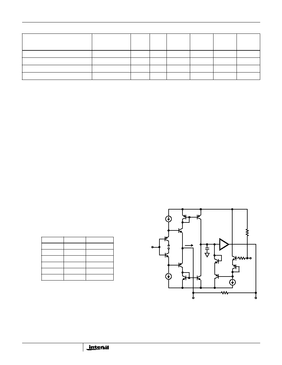
Clamp Circuitry
Figure 1 shows a simplified schematic of the HFA1130 input
stage, and the high clamp (V
H
) circuitry. As with all current
feedback amplifiers, there is a unity gain buffer (Q
X1
- Q
X2
)
between the positive and negative inputs. This buffer forces -IN to
track +IN, and sets up a slewing current of (V
-IN
- V
OUT
)/R
F
.
This current is mirrored onto the high impedance node (Z) by
Q
X3
-Q
X4
, where it is converted to a voltage and fed to the output
via another unity gain buffer. If no clamping is utilized, the high
impedance node may swing within the limits defined by Q
P4
and
Q
N4
. Note that when the output reaches it's quiescent value, the
current flowing through -IN is reduced to only that small current
(-I
BIAS
) required to keep the output at the final voltage.
Tracing the path from V
H
to Z illustrates the effect of the
clamp voltage on the high impedance node. V
H
decreases
by 2V
BE
(Q
N6
and Q
P6
) to set up the base voltage on Q
P5
.
Q
P5
begins to conduct whenever the high impedance node
Negative Clamp Range
B
25
-
-5.0 to +2.0
-
V
Positive Clamp Range
B
25
-
-2.0 to +5.0
-
V
Clamp Input Bias Current
A
25
-
50
200
µ
A
Clamp Input Bandwidth
V
H
or V
L
= 100mV
P-P
B
25
-
500
-
MHz
NOTES:
2. Test Level: A. Production Tested; B. Typical or Guaranteed Limit Based on Characterization; C. Design Typical for Information Only.
3. See Typical Performance Curves for more information.
Electrical Specifications
V
SUPPLY
=
±
5V, A
V
= +1, R
F
= 510
, R
L
= 100
, Unless Otherwise Specified (Continued)
PARAMETER
TEST
CONDITIONS
(NOTE 2)
TEST
LEVEL
TEMP.
(
o
C)
MIN
TYP
MAX
UNITS
A
CL
R
F
(
)
BW (MHz)
+1
510
850
-1
430
580
+2
360
670
+5
150
520
+10
180
240
+19
270
125
+1
+IN
V-
V+
Q
P1
Q
N1
V-
Q
N3
Q
P3
Q
P4
Q
N2
Q
P2
Q
N4
Q
P5
Q
N5
Z
V+
-IN
V
OUT
I
CLAMP
R
F
(EXTERNAL)
Q
P6
Q
N6
V
H
R
1
50K
(30K
FOR V
L
)
200
FIGURE 1. HFA1130 SIMPLIFIED V
H
CLAMP CIRCUITRY
HFA1130

5
reaches a voltage equal to Q
P5
's base + 2V
BE
(Q
P5
and
Q
N5
). Thus, Q
P5
clamps node Z whenever Z reaches V
H
.
R
1
provides a pull-up network to ensure functionality with the
clamp inputs floating. A similar description applies to the
symmetrical low clamp circuitry controlled by V
L
.
When the output is clamped, the negative input continues to
source a slewing current (I
CLAMP
) in an attempt to force the
output to the quiescent voltage defined by the input. Q
P5
must sink this current while clamping, because the -IN
current is always mirrored onto the high impedance node.
The clamping current is calculated as (V
-IN
- V
OUT
)/R
F
. As
an example, a unity gain circuit with V
IN
= 2V, V
H
= 1V, and
R
F
= 510
would have I
CLAMP
= (2-1)/510
= 1.96mA.
Note that I
CC
will increase by I
CLAMP
when the output is
clamp limited.
Clamp Accuracy
The clamped output voltage will not be exactly equal to the
voltage applied to V
H
or V
L
. Offset errors, mostly due to V
BE
mismatches, necessitate a clamp accuracy parameter which is
found in the device specifications. Clamp accuracy is a function
of the clamping conditions. Referring again to Figure 1, it can
be seen that one component of clamp accuracy is the V
BE
mismatch between the Q
X6
transistors, and the Q
X5
transistors. If the transistors always ran at the same current
level there would be no V
BE
mismatch, and no contribution to
the inaccuracy. The Q
X6
transistors are biased at a constant
current, but as described earlier, the current through Q
X5
is
equivalent to I
CLAMP
. V
BE
increases as I
CLAMP
increases,
causing the clamped output voltage to increase as well.
I
CLAMP
is a function of the overdrive level
(V
-IN
-V
OUTCLAMPED
) and R
F
,so clamp accuracy degrades as
the overdrive increases, or as R
F
decreases. As an example,
the specified accuracy of
±
60mV for a 2X overdrive with
R
F
= 510
degrades to
±
220mV for R
F
= 240
at the same
overdrive, or to
±
250mV for a 3X overdrive with R
F
= 510
.
Consideration must also be given to the fact that the clamp
voltages have an effect on amplifier linearity. The
"Nonlinearity Near Clamp Voltage" curve in the data sheet
illustrates the impact of several clamp levels on linearity.
Clamp Range
Unlike some competitor devices, both V
H
and V
L
have usable
ranges that cross 0V. While V
H
must be more positive than V
L
,
both may be positive or negative, within the range restrictions
indicated in the specifications. For example, the HFA1130 could
be limited to ECL output levels by setting V
H
= -0.8V and
V
L
= -1.8V. V
H
and V
L
may be connected to the same voltage
(GND for instance) but the result won't be in a DC output
voltage from an AC input signal. A 150 - 200mV AC signal will
still be present at the output.
Recovery from Overdrive
The output voltage remains at the clamp level as long as the
overdrive condition remains. When the input voltage drops
below the overdrive level (V
CLAMP
/A
VCL
) the amplifier will
return to linear operation. A time delay, known as the
Overdrive Recovery Time, is required for this resumption of
linear operation. The plots of "Unclamped Performance" and
"Clamped Performance" highlight the HFA1130's
subnanosecond recovery time. The difference between the
unclamped and clamped propagation delays is the overdrive
recovery time. The appropriate propagation delays are 4.0ns
for the unclamped pulse, and 4.8ns for the clamped (2X
overdrive) pulse yielding an overdrive recovery time of
800ps. The measurement uses the 90% point of the output
transition to ensure that linear operation has resumed.
Note: The propagation delay illustrated is dominated by the
fixturing. The delta shown is accurate, but the true HFA1130
propagation delay is 500ps.
Use of Die in Hybrid Applications
This amplifier is designed with compensation to negate the
package parasitics that typically lead to instabilities. As a
result, the use of die in hybrid applications results in
overcompensated performance due to lower parasitic
capacitances. Reducing R
F
below the recommended values
for packaged units will solve the problem. For A
V
= +2 the
recommended starting point is 300
, while unity gain
applications should try 400
.
PC Board Layout
The frequency performance of this amplifier depends a great
deal on the amount of care taken in designing the PC board.
The use of low inductance components such as chip
resistors and chip capacitors is strongly recommended,
while a solid ground plane is a must!
Attention should be given to decoupling the power supplies.
A large value (10
µ
F) tantalum in parallel with a small value
chip (0.1
µ
F) capacitor works well in most cases.
Terminated microstrip signal lines are recommended at the
input and output of the device. Output capacitance, such as
that resulting from an improperly terminated transmission
line will degrade the frequency response of the amplifier and
may cause oscillations. In most cases, the oscillation can be
avoided by placing a resistor in series with the output.
Care must also be taken to minimize the capacitance to
ground seen by the amplifier's inverting input. The larger this
capacitance, the worse the gain peaking, resulting in pulse
overshoot and possible instability. To this end, it is
recommended that the ground plane be removed under
traces connected to pin 2, and connections to pin 2 should
be kept as short as possible.
An example of a good high frequency layout is the
Evaluation Board shown below.
HFA1130