 | –≠–ª–µ–∫—Ç—Ä–æ–Ω–Ω—ã–π –∫–æ–º–ø–æ–Ω–µ–Ω—Ç: HFA1145IP | –°–∫–∞—á–∞—Ç—å:  PDF PDF  ZIP ZIP |

1
CAUTION: These devices are sensitive to electrostatic discharge; follow proper IC Handling Procedures.
1-888-INTERSIL or 321-724-7143
|
Copyright
©
Intersil Corporation 1999
HFA1145
330MHz, Low Power, Current Feedback
Video Operational Amplifier with Output
Disable
The HFA1145 is a high speed, low power current feedback
amplifier built with Intersil's proprietary complementary
bipolar UHF-1 process.
This amplifier features a TTL/CMOS compatible disable
control, pin 8, which when pulled low reduces the supply
current and forces the output into a high impedance state.
This allows easy implementation of simple, low power video
switching and routing systems. Component and composite
video systems also benefit from this op amp's excellent gain
flatness, and good differential gain and phase specifications.
Multiplexed A/D applications will also find the HFA1145
useful as the A/D driver/multiplexer.
The HFA1145 is a low power, high performance upgrade for
the CLC410.
For Military grade product, please refer to the HFA1145/883
data sheet
.
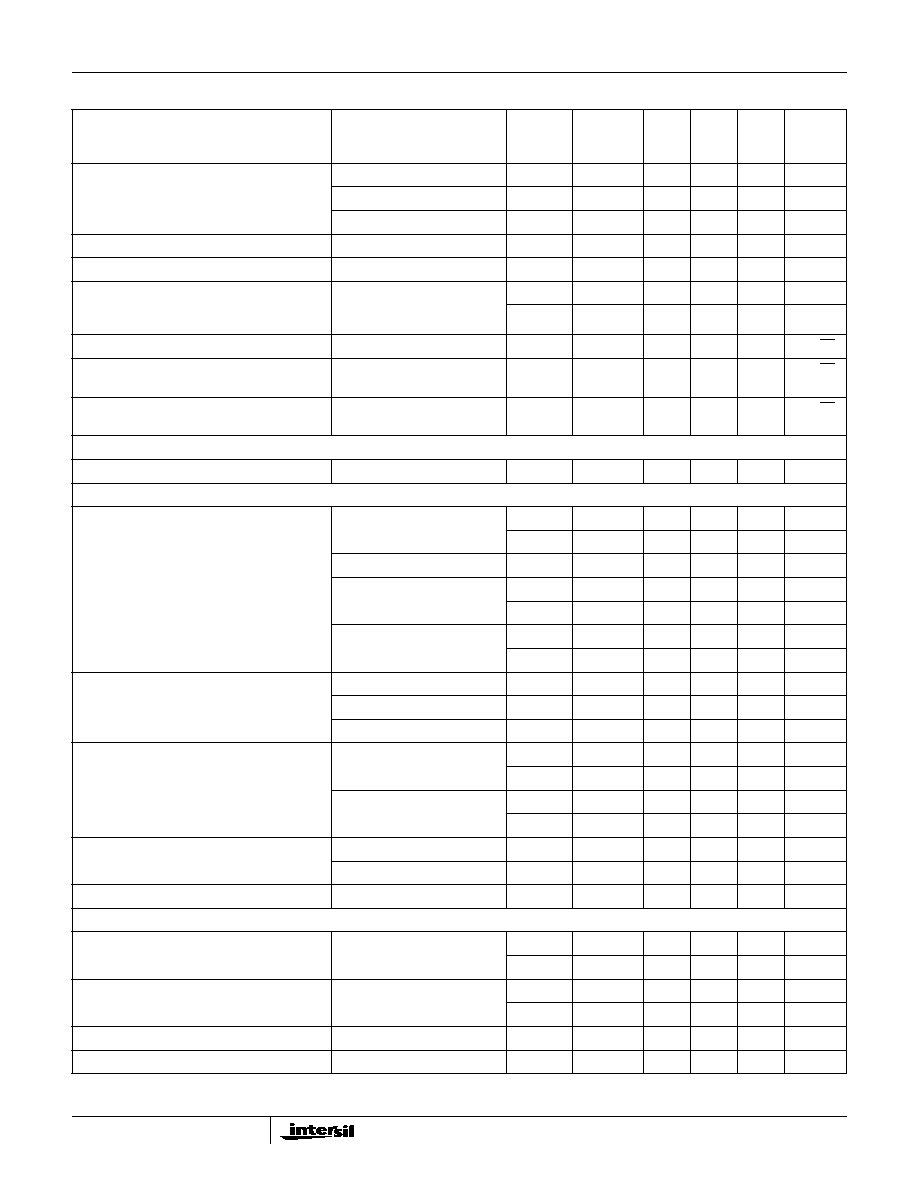
Pinout
HFA1145
(PDIP, SOIC)
TOP VIEW
Features
∑ Low Supply Current . . . . . . . . . . . . . . . . . . . . . . . . 5.8mA
∑ High Input Impedance . . . . . . . . . . . . . . . . . . . . . . . 1M
∑ Wide -3dB Bandwidth. . . . . . . . . . . . . . . . . . . . . . 330MHz
∑ Very Fast Slew Rate . . . . . . . . . . . . . . . . . . . . . . 1000V/
µ
s
∑ Gain Flatness (to 75MHz) . . . . . . . . . . . . . . . . . .
±
0.1dB
∑ Differential Gain . . . . . . . . . . . . . . . . . . . . . . . . . . . 0.02%
∑ Differential Phase . . . . . . . . . . . . . . . . . . . . 0.03 Degrees
∑ Output Enable/Disable Time. . . . . . . . . . . . . . 180ns/35ns
∑ Pin Compatible Upgrade for CLC410
Applications
∑ Flash A/D Drivers
∑ Video Switching and Routing
∑ Professional Video Processing
∑ Video Digitizing Boards/Systems
∑ Multimedia Systems
∑ RGB Preamps
∑ Medical Imaging
∑ Hand Held and Miniaturized RF Equipment
∑ Battery Powered Communications
Ordering Information
PART NUMBER
(BRAND)
TEMP. RANGE
(
o
C)
PACKAGE
PKG.
NO.
HFA1145IP
-40 to 85
8 Ld PDIP
E8.3
HFA1145IB
(H1145I)
-40 to 85
8 Ld SOIC
M8.15
HFA11XXEVAL
DIP Evaluation Board for High Speed Op Amps
NC
-IN
+IN
V-
1
2
3
4
8
7
6
5
DISABLE
V+
OUT
NC
-
+
Data Sheet
September 1998
File Number
3955.3

2
Absolute Maximum Ratings
Thermal Information
Voltage Between V+ and V- . . . . . . . . . . . . . . . . . . . . . . . . . . . . 11V
DC Input Voltage . . . . . . . . . . . . . . . . . . . . . . . . . . . . . . . . V
SUPPLY
Differential Input Voltage . . . . . . . . . . . . . . . . . . . . . . . . . . . . . . . 8V
Output Current (Note 1) . . . . . . . . . . . . . . . . .Short Circuit Protected
30mA Continuous
60mA
50% Duty Cycle
ESD Rating . . . . . . . . . . . . . . . . . . . . . . . . . . . . . . . . . . . . . . >600V
Operating Conditions
Temperature Range . . . . . . . . . . . . . . . . . . . . . . . . . . -40
o
C to 85
o
C
Thermal Resistance (Typical, Note 2)
JA
(
o
C/W)
PDIP Package . . . . . . . . . . . . . . . . . . . . . . . . . . . . .
130
SOIC Package . . . . . . . . . . . . . . . . . . . . . . . . . . . . .
170
Maximum Junction Temperature (Die Only) . . . . . . . . . . . . . . . .175
o
C
Maximum Junction Temperature (Plastic Package) . . . . . . . .150
o
C
Maximum Storage Temperature Range . . . . . . . . . . -65
o
C to 150
o
C
Maximum Lead Temperature (Soldering 10s) . . . . . . . . . . . . 300
o
C
(SOIC - Lead Tips Only)
CAUTION: Stresses above those listed in "Absolute Maximum Ratings" may cause permanent damage to the device. This is a stress only rating and operation of the
device at these or any other conditions above those indicated in the operational sections of this specification is not implied.
NOTES:
1. Output is short circuit protected to ground. Brief short circuits to ground will not degrade reliability, however continuous (100% duty cycle) output
current must not exceed 30mA for maximum reliability.
2.
JA
is measured with the component mounted on an evaluation PC board in free air.
Electrical Specifications
V
SUPPLY
=
±
5V, A
V
= +1, R
F
= 510
, R
L
= 100
,
Unless Otherwise Specified
PARAMETER
TEST CONDITIONS
(NOTE 3)
TEST
LEVEL
TEMP.
(
o
C)
MIN
TYP
MAX
UNITS
INPUT CHARACTERISTICS
Input Offset Voltage
A
25
-
2
5
mV
A
Full
-
3
8
mV
Average Input Offset Voltage Drift
B
Full
-
1
10
µ
V/
o
C
Input Offset Voltage
Common-Mode Rejection Ratio
V
CM
=
±
1.8V
A
25
47
50
-
dB
V
CM
=
±
1.8V
A
85
45
48
-
dB
V
CM
=
±
1.2V
A
-40
45
48
-
dB
Input Offset Voltage
Power Supply Rejection Ratio
V
PS
=
±
1.8V
A
25
50
54
-
dB
V
PS
=
±
1.8V
A
85
47
50
-
dB
V
PS
=
±
1.2V
A
-40
47
50
-
dB
Non-Inverting Input Bias Current
A
25
-
6
15
µ
A
A
Full
-
10
25
µ
A
Non-Inverting Input Bias Current Drift
B
Full
-
5
60
nA/
o
C
Non-Inverting Input Bias Current
Power Supply Sensitivity
V
PS
=
±
1.8V
A
25
-
0.5
1
µ
A/V
V
PS
=
±
1.8V
A
85
-
0.8
3
µ
A/V
V
PS
=
±
1.2V
A
-40
-
0.8
3
µ
A/V
Non-Inverting Input Resistance
V
CM
=
±
1.8V
A
25
0.8
1.2
-
M
V
CM
=
±
1.8V
A
85
0.5
0.8
-
M
V
CM
=
±
1.2V
A
-40
0.5
0.8
-
M
Inverting Input Bias Current
A
25
-
2
7.5
µ
A
A
Full
-
5
15
µ
A
Inverting Input Bias Current Drift
B
Full
-
60
200
nA/
o
C
Inverting Input Bias Current
Common-Mode Sensitivity
V
CM
=
±
1.8V
A
25
-
3
6
µ
A/V
V
CM
=
±
1.8V
A
85
-
4
8
µ
A/V
V
CM
=
±
1.2V
A
-40
-
4
8
µ
A/V
HFA1145
3
Inverting Input Bias Current
Power Supply Sensitivity
V
PS
=
±
1.8V
A
25
-
2
5
µ
A/V
V
PS
=
±
1.8V
A
85
-
4
8
µ
A/V
V
PS
=
±
1.2V
A
-40
-
4
8
µ
A/V
Inverting Input Resistance
C
25
-
60
-
Input Capacitance
C
25
-
1.6
-
pF
Input Voltage Common Mode Range
(Implied by V
IO
CMRR, +R
IN
, and -I
BIAS
CMS
tests)
A
25, 85
±
1.8
±
2.4
-
V
A
-40
±
1.2
±
1.7
-
V
Input Noise Voltage Density (Note 6)
f = 100kHz
B
25
-
3.5
-
nV/
Hz
Non-Inverting Input Noise Current Density
(Note 6)
f = 100kHz
B
25
-
2.5
-
pA/
Hz
Inverting Input Noise Current Density
(Note 6)
f = 100kHz
B
25
-
20
-
pA/
Hz
TRANSFER CHARACTERISTICS
Open Loop Transimpedance Gain
A
V
= -1
C
25
-
500
-
k
AC CHARACTERISTICS
R
F
= 510
, Unless Otherwise Specified
-3dB Bandwidth
(V
OUT
= 0.2V
P-P
, Note 6)
A
V
= +1, +R
S
= 510
B
25
-
270
-
MHz
B
Full
-
240
-
MHz
A
V
= -1, R
F
= 425
B
25
-
300
-
MHz
A
V
= +2
B
25
-
330
-
MHz
B
Full
-
260
-
MHz
A
V
= +10, R
F
= 180
B
25
-
130
-
MHz
B
Full
-
90
-
MHz
Full Power Bandwidth
(V
OUT
= 5V
P-P
at A
V
= +2/-1,
4V
P-P
at A
V
= +1, Note 6)
A
V
= +1, +R
S
= 510
B
25
-
135
-
MHz
A
V
= -1
B
25
-
140
-
MHz
A
V
= +2
B
25
-
115
-
MHz
Gain Flatness
(A
V
= +2, V
OUT
= 0.2V
P-P
, Note 6)
To 25MHz
B
25
-
±
0.03
-
dB
B
Full
-
±
0.04
-
dB
To 75MHz
B
25
-
±
0.11
-
dB
B
Full
-
±
0.22
-
dB
Gain Flatness
(A
V
= +1, +R
S
= 510
, V
OUT
= 0.2V
P-P
, Note 6)
To 25MHz
B
25
-
±
0.03
-
dB
To 75MHz
B
25
-
±
0.09
-
dB
Minimum Stable gain
A
Full
-
1
-
V/V
OUTPUT CHARACTERISTICS A
V
= +2, R
F
= 510
, Unless Otherwise Specified
Output Voltage Swing
(Note 6)
A
V
= -1, R
L
= 100
A
25
±
3
±
3.4
-
V
A
Full
±
2.8
±
3
-
V
Output Current
(Note 6)
A
V
= -1, R
L
= 50
A
25, 85
50
60
-
mA
A
-40
28
42
-
mA
Output Short Circuit Current
B
25
-
90
-
mA
Closed Loop Output Impedance (Note 6)
DC
B
25
-
0.08
-
Electrical Specifications
V
SUPPLY
=
±
5V, A
V
= +1, R
F
= 510
, R
L
= 100
,
Unless Otherwise Specified (Continued)
PARAMETER
TEST CONDITIONS
(NOTE 3)
TEST
LEVEL
TEMP.
(
o
C)
MIN
TYP
MAX
UNITS
HFA1145

4
Second Harmonic Distortion
(V
OUT
= 2V
P-P
, Note 6)
10MHz
B
25
-
-48
-
dBc
20MHz
B
25
-
-44
-
dBc
Third Harmonic Distortion
(V
OUT
= 2V
P-P
, Note 6)
10MHz
B
25
-
-50
-
dBc
20MHz
B
25
-
-45
-
dBc
Reverse Isolation (S
12
, Note 6)
30MHz
B
25
-
-55
-
dB
TRANSIENT CHARACTERISTICS
A
V
= +2, R
F
= 510
,
Unless Otherwise Specified
Rise and Fall Times
V
OUT
= 0.5V
P-P
B
25
-
1.1
-
ns
B
Full
-
1.4
-
ns
Overshoot (Note 4)
(V
OUT
= 0 to 0.5V, V
IN
t
RISE
= 1ns)
+OS
B
25
-
3
-
%
-OS
B
25
-
5
-
%
Overshoot (Note 4)
(V
OUT
= 0.5V
P-P
, V
IN
t
RISE
= 1ns)
+OS
B
25
-
3
-
%
-OS
B
25
-
11
-
%
Slew Rate
(V
OUT
= 4V
P-P
, A
V
= +1, +R
S
= 510
)
+SR
B
25
-
1000
-
V/
µ
s
B
Full
-
975
-
V/
µ
s
-SR (Note 5)
B
25
-
650
-
V/
µ
s
B
Full
-
580
-
V/
µ
s
Slew Rate
(V
OUT
= 5V
P-P
, A
V
= +2)
+SR
B
25
-
1400
-
V/
µ
s
B
Full
-
1200
-
V/
µ
s
-SR (Note 5)
B
25
-
800
-
V/
µ
s
B
Full
-
700
-
V/
µ
s
Slew Rate
(V
OUT
= 5V
P-P
, A
V
= -1)
+SR
B
25
-
2100
-
V/
µ
s
B
Full
-
1900
-
V/
µ
s
-SR (Note 5)
B
25
-
1000
-
V/
µ
s
B
Full
-
900
-
V/
µ
s
Settling Time
(V
OUT
= +2V to 0V step, Note 6)
To 0.1%
B
25
-
15
-
ns
To 0.05%
B
25
-
23
-
ns
To 0.02%
B
25
-
30
-
ns
Overdrive Recovery Time
V
IN
=
±
2V
B
25
-
8.5
-
ns
VIDEO CHARACTERISTICS
A
V
= +2, R
F
= 510
,
Unless Otherwise Specified
Differential Gain
(f = 3.58MHz)
R
L
= 150
B
25
-
0.02
-
%
R
L
= 75
B
25
-
0.03
-
%
Differential Phase
(f = 3.58MHz)
R
L
= 150
B
25
-
0.03
-
Degrees
R
L
= 75
B
25
-
0.05
-
Degrees
DISABLE CHARACTERISTICS
Disabled Supply Current
V
DISABLE
= 0V
A
Full
-
3
4
mA
DISABLE Input Logic Low
A
Full
-
-
0.8
V
DISABLE Input Logic High
A
25, 85
2.0
-
-
V
A
-40
2.4
-
-
V
DISABLE Input Logic Low Current
V
DISABLE
= 0V
A
Full
-
100
200
µ
A
Electrical Specifications
V
SUPPLY
=
±
5V, A
V
= +1, R
F
= 510
, R
L
= 100
,
Unless Otherwise Specified (Continued)
PARAMETER
TEST CONDITIONS
(NOTE 3)
TEST
LEVEL
TEMP.
(
o
C)
MIN
TYP
MAX
UNITS
HFA1145
5
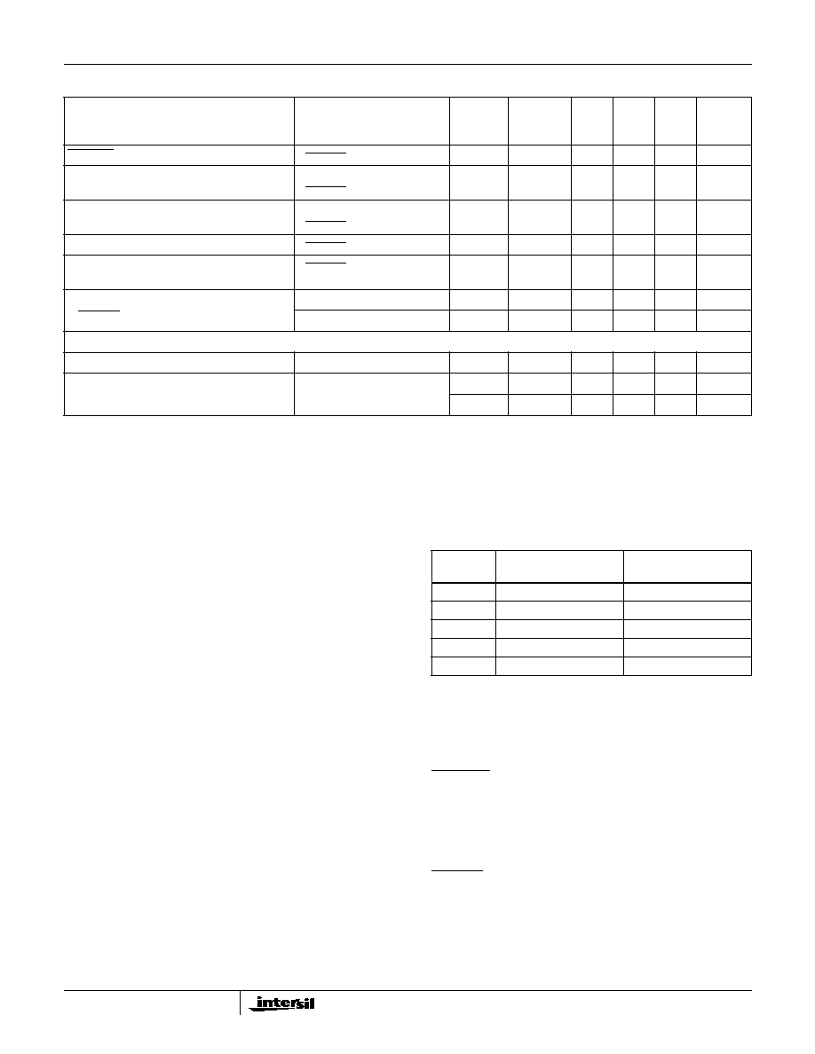
Application Information
Optimum Feedback Resistor
Although a current feedback amplifier's bandwidth
dependency on closed loop gain isn't as severe as that of a
voltage feedback amplifier, there can be an appreciable
decrease in bandwidth at higher gains. This decrease may be
minimized by taking advantage of the current feedback
amplifier's unique relationship between bandwidth and R
F
. All
current feedback amplifiers require a feedback resistor, even
for unity gain applications, and R
F
, in conjunction with the
internal compensation capacitor, sets the dominant pole of the
frequency response. Thus, the amplifier's bandwidth is
inversely proportional to R
F
. The HFA1145 design is optimized
for R
F
= 510
at a gain of +2. Decreasing R
F
decreases
stability, resulting in excessive peaking and overshoot (Note:
Capacitive feedback will cause the same problems due to the
feedback impedance decrease at higher frequencies). At
higher gains, however, the amplifier is more stable so R
F
can
be decreased in a trade-off of stability for bandwidth.
The table below lists recommended R
F
values for various
gains, and the expected bandwidth. For a gain of +1, a
resistor (
+
R
S
) in series with +IN is required to reduce gain
peaking and increase stability.
Non-inverting Input Source Impedance
For best operation, the DC source impedance seen by the
non-inverting input should be
50
.
This is especially
important in inverting gain configurations where the non-
inverting input would normally be connected directly to GND.
DISABLE Input TTL Compatibility
The HFA1145 derives an internal GND reference for the
digital circuitry as long as the power supplies are
symmetrical about GND. With symmetrical supplies the
digital switching threshold (V
TH
= (V
IH
+ V
IL
)/2 = (2.0 +
0.8)/2) is 1.4V, which ensures the TTL compatibility of the
DISABLE input. If asymmetrical supplies (e.g. +10V, 0V) are
utilized, the switching threshold becomes:
and the V
IH
and V
IL
levels will be V
TH
±
0.6V, respectively.
DISABLE Input Logic High Current
V
DISABLE
= 5V
A
Full
-
1
15
µ
A
Output Disable Time (Note 6)
V
IN
=
±
1V,
V
DISABLE
= 2.4V to 0V
B
25
-
35
-
ns
Output Enable Time (Note 6)
V
IN
=
±
1V,
V
DISABLE
= 0V to 2.4V
B
25
-
180
-
ns
Disabled Output Capacitance
V
DISABLE
= 0V
B
25
-
2.5
-
pF
Disabled Output Leakage
V
DISABLE
= 0V, V
IN
=
2V,
V
OUT
=
±
3V
A
Full
-
3
10
µ
A
Off Isolation
(V
DISABLE
= 0V, V
IN
= 1V
P-P
, Note 6)
At 5MHz
B
25
-
-75
-
dB
At 25MHz
B
25
-
-60
-
dB
POWER SUPPLY CHARACTERISTICS
Power Supply Range
C
25
±
4.5
-
±
5.5
V
Power Supply Current (Note 6)
A
25
-
5.8
6.1
mA
A
Full
-
5.9
6.3
mA
NOTES:
3. Test Level: A. Production Tested; B. Typical or Guaranteed Limit Based on Characterization; C. Design Typical for Information Only.
4. Undershoot dominates for output signal swings below GND (e.g. 0.5V
P-P
), yielding a higher overshoot limit compared to the V
OUT
= 0 to 0.5V
condition. See the "Application Information" section for details.
5. Slew rates are asymmetrical if the output swings below GND (e.g. a bipolar signal). Positive unipolar output signals have symmetric positive and
negative slew rates comparable to the +SR specification. See the "Application Information" section, and the pulse response graphs for details.
6. See Typical Performance Curves for more information.
Electrical Specifications
V
SUPPLY
=
±
5V, A
V
= +1, R
F
= 510
, R
L
= 100
,
Unless Otherwise Specified (Continued)
PARAMETER
TEST CONDITIONS
(NOTE 3)
TEST
LEVEL
TEMP.
(
o
C)
MIN
TYP
MAX
UNITS
±
GAIN
(A
CL
)
R
F
(
)
BANDWIDTH
(MHz)
-1
425
300
+1
510 (+RS = 510
)
270
+2
510
330
+5
200
300
+10
180
130
V
TH
V+
V-
+
2
-------------------
1.4V
+
=
HFA1145