 | ÐлекÑÑоннÑй компоненÑ: HFA1150IB | СкаÑаÑÑ:  PDF PDF  ZIP ZIP |
Äîêóìåíòàöèÿ è îïèñàíèÿ www.docs.chipfind.ru
TM
1
File Number
4836
HFA1150
700MHz, SOT-23, Low Distortion Current
Feedback Operational Amplifier
The HFA1150 is a high-speed, wideband, fast settling op
amp built with Intersil's proprietary complementary bipolar
UHF-1 process. The current feedback architecture delivers
superb bandwidth even at very high gains (>300MHz at
A
V
= 10), and the low distortion and excellent video
parameters make this amplifier ideal for communication and
professional video applications.
Though specified for
±
5V operation, the HFA1150 operates
with single supply voltages as low as 4.5V, and requires only
3.4mA of I
cc
in 5V applications (see Application Information
section, and Application Note AN9891).
For a lower power amplifier in a SOT-23 package, please
refer to the HFA1155 data sheet.
Features
· Low Distortion (5MHz, HD2). . . . . . . . . . . . . . . . . . -67dBc
· -3dB Bandwidth . . . . . . . . . . . . . . . . . . . . . . . . . . 700MHz
· High Slew Rate. . . . . . . . . . . . . . . . . . . . . . . . . . 2700V/
µ
s
· Fast Settling Time (0.1%) . . . . . . . . . . . . . . . . . . . . . 20ns
· Excellent Gain Flatness . . . . . . . . . .
±
0.05dB to 100MHz
· High Output Current . . . . . . . . . . . . . . . . . . . . . . . . . 60mA
· Fast Overdrive Recovery . . . . . . . . . . . . . . . . . . . . . <5ns
· Operates with 5V Single Supply (See AN9891)
Applications
· Video Switching and Routing
· Pulse and Video Amplifiers
· RF/IF Signal Processing
· Flash A/D Driver
· Medical Imaging Systems
· Related Literature
- AN9420, Current Feedback Theory
- AN9891, Single 5V Supply Operation
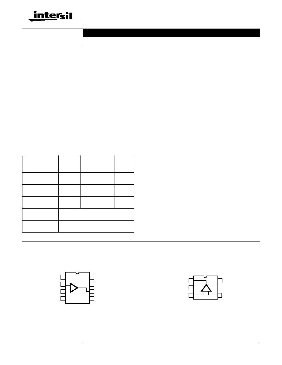
Pinouts
Ordering Information
PART NUMBER
(BRAND)
TEMP.
RANGE
(
o
C)
PACKAGE
PKG. NO.
HFA1150IB
(H1150I)
-40 to 85
8 Ld SOIC
M8.15
HFA1150IB96
(H1150I)
-40 to 85
8 Ld SOIC
Tape and Reel
M8.15
HFA1150IH96
(1150)
-40 to 85
5 Ld SOT-23 Tape
and Reel
P5.064
HFA11XXEVAL
DIP Evaluation Board for High-Speed Op
Amps
OPAMPSOT23EVAL SOT-23 Evaluation Board for High-Speed Op
Amps
HFA1150
(SOIC)
TOP VIEW
HFA1150
(SOT23)
TOP VIEW
NC
-IN
+IN
V-
1
2
3
4
8
7
6
5
NC
V+
OUT
NC
+
-
1
2
3
5
4
+ -
V-
V+
-IN
+IN
OUT
Data Sheet
March 2000
CAUTION: These devices are sensitive to electrostatic discharge; follow proper IC Handling Procedures.
1-888-INTERSIL or 321-724-7143
|
Intersil and Design is a trademark of Intersil Corporation.
|
Copyright
©
Intersil Corporation 2000
2
Absolute Maximum Ratings
T
A
= 25
o
C
Thermal Information
Voltage Between V+ and V- . . . . . . . . . . . . . . . . . . . . . . . . . . . . 12V
Input Voltage . . . . . . . . . . . . . . . . . . . . . . . . . . . . . . . . . . . V
SUPPLY
Differential Input Voltage . . . . . . . . . . . . . . . . . . . . . . . . . . . . . . . 5V
Output Current (50% Duty Cycle) . . . . . . . . . . . . . . . . . . . . . . 60mA
ESD Rating
Human Body Model (Per MIL-STD-883 Method 3015.7) . . . 600V
Operating Conditions
Temperature Range . . . . . . . . . . . . . . . . . . . . . . . . . . -40
o
C to 85
o
C
Thermal Resistance (Typical, Note 1)
JA
(
o
C/W)
SOIC Package . . . . . . . . . . . . . . . . . . .
175
SOT-23 Package . . . . . . . . . . . . . . . . .
225
Moisture Sensitivity (see Technical Brief TB363)
SOIC Package . . . . . . . . . . . . . . . . . . . . . . . . . . . . . . . . . . Level 1
SOT-23 Package . . . . . . . . . . . . . . . . . . . . . . . . . . . . . . . . Level 1
Maximum Junction Temperature (Plastic Package) . . . . . . . . .150
o
C
Maximum Storage Temperature Range . . . . . . . . . . -65
o
C to 150
o
C
Maximum Lead Temperature (Soldering 10s) . . . . . . . . . . . . 300
o
C
(Lead Tips Only)
CAUTION: Stresses above those listed in "Absolute Maximum Ratings" may cause permanent damage to the device. This is a stress only rating and operation of the
device at these or any other conditions above those indicated in the operational sections of this specification is not implied.
NOTE:
1.
JA
is measured with the component mounted on an evaluation PC board in free air.
Electrical Specifications
V
SUPPLY
=
±
5V, A
V
= 1, R
F
= 510
, R
L
= 100
, Unless Otherwise Specified
PARAMETER
TEST
CONDITIONS
(NOTE 2)
TEST
LEVEL
TEMP.
(
o
C)
HFA1150IB (SOIC)
HFA1150IH (SOT-23)
UNITS
MIN
TYP
MAX
MIN
TYP
MAX
INPUT CHARACTERISTICS
Input Offset Voltage (Note 3)
A
25
-
2
6
-
2
6
mV
A
Full
-
-
10
-
-
10
mV
Input Offset Voltage Drift
C
Full
-
10
-
-
10
-
µ
V/
o
C
V
IO
CMRR
V
CM
=
±
2V
A
25
40
46
-
40
46
-
dB
A
Full
38
-
-
38
-
-
dB
V
IO
PSRR
V
S
=
±
1.25V
A
25
45
50
-
45
50
-
dB
A
Full
42
-
-
42
-
-
dB
Non-Inverting Input Bias Current
(Note 3)
+IN = 0V
A
25
-
25
40
-
25
40
µ
A
A
Full
-
-
65
-
-
65
µ
A
+I
BIAS
Drift
C
Full
-
40
-
-
40
-
nA/
o
C
+I
BIAS
CMS
V
CM
=
±
2V
A
25
-
20
40
-
20
40
µ
A/V
A
Full
-
-
50
-
-
50
µ
A/V
Inverting Input Bias Current (Note 3)
-IN = 0V
A
25
-
12
50
-
12
50
µ
A
A
Full
-
-
60
-
-
60
µ
A
-I
BIAS
Drift
C
Full
-
40
-
-
40
-
nA/
o
C
-I
BIAS
CMS
V
CM
=
±
2V
A
25
-
1
7
-
1
7
µ
A/V
A
Full
-
-
10
-
-
10
µ
A/V
-I
BIAS
PSS
V
S
=
±
1.25V
A
25
-
6
15
-
6
15
µ
A/V
A
Full
-
-
27
-
-
27
µ
A/V
Non-Inverting Input Resistance
A
25
25
50
-
25
50
-
k
Inverting Input Resistance
C
25
-
25
-
-
25
-
Input Capacitance (Either Input)
B
25
-
2
-
-
2
-
pF
Input Common Mode Range
C
Full
±
2.5
±
3.0
-
±
2.5
±
3.0
-
V
Input Noise Voltage (Note 3)
100kHz
B
25
-
4.7
-
-
4.7
-
nV/
Hz
+Input Noise Current (Note 3)
100kHz
B
25
-
20
-
-
20
-
pA/
Hz
-Input Noise Current (Note 3)
100kHz
B
25
-
40
-
-
40
-
pA/
Hz
TRANSFER CHARACTERISTICS
Open Loop Transimpedance Gain (Note 3)
B
25
-
450
-
-
450
-
k
Minimum Stable Gain
A
Full
1
-
-
1
-
-
V/V
HFA1150
3
AC CHARACTERISTICS
A
V
= +2, (Note 4) Unless Otherwise Specified
-3dB Bandwidth
(V
OUT
= 0.2V
P-P
, Note 3)
A
V
= -1
B
25
-
650
-
-
540
-
MHz
A
V
= +1
B
25
-
600
-
-
500
-
MHz
A
V
= +2
B
25
-
700
-
-
540
-
MHz
-3dB Bandwidth (V
OUT
= 2V
P-P
)
A
V
= +2
B
25
-
375
-
-
350
-
MHz
Gain Flatness
(V
OUT
= 0.2V
P-P
, Note 3)
To 25MHz
B
25
-
±
0.03
-
-
±
0.05
-
dB
To 50MHz
B
25
-
±
0.04
-
-
±
0.08
-
dB
To 100MHz
B
25
-
±
0.05
-
-
±
0.1
-
dB
Full Power Bandwidth
(V
OUT
= 5V
P-P
, Note 3)
A
V
= +1
B
25
-
100
-
-
90
-
MHz
A
V
= +2
B
25
-
175
-
-
160
-
MHz
OUTPUT CHARACTERISTICS
A
V
= +2, (Note 4) Unless Otherwise Specified
Output Voltage
A
V
= -1
A
25
±
3.0
±
3.3
-
±
3.0
±
3.3
-
V
A
Full
±
2.5
±
3.0
-
±
2.5
±
3.0
-
V
Output Current
R
L
= 50
, A
V
= -1
A
25, 85
±
50
±
60
-
±
50
±
60
-
mA
A
-40
±
35
±
50
-
±
35
±
50
-
mA
DC Closed Loop Output Impedance (Note 3)
B
25
-
0.07
-
-
0.07
-
2nd Harmonic Distortion (Note 3)
5MHz, V
OUT
= 2V
P-P
B
25
-
-67
-
-
-67
-
dBc
30MHz, V
OUT
= 2V
P-P
B
25
-
-53
-
-
-53
-
dBc
3rd Harmonic Distortion (Note 3)
5MHz, V
OUT
= 2V
P-P
B
25
-
<-100
-
-
<-100
-
dBc
30MHz, V
OUT
= 2V
P-P
B
25
-
-76
-
-
-76
-
dBc
TRANSIENT CHARACTERISTICS
A
V
= +2, (Note 4) Unless Otherwise Specified
Rise and Fall Times
V
OUT
= 0.5V
P-P
B
25
-
0.6
-
-
0.7
-
ns
Overshoot
V
OUT
= 0.5V
P-P
B
25
-
12
-
-
12
-
%
Slew Rate (V
OUT
= 5V
P-P
)
A
V
= -1
B
25
-
2700
-
-
2500
-
V/
µ
s
A
V
= +1
B
25
-
750
-
-
700
-
V/
µ
s
A
V
= +2
B
25
-
1300
-
-
1200
-
V/
µ
s
Settling Time (V
OUT
= 2V to 0V, Note 3)
To 0.1%
B
25
-
20
-
-
30
-
ns
To 0.05%
B
25
-
33
-
-
37
-
ns
To 0.01%
B
25
-
55
-
-
60
-
ns
Overdrive Recovery Time
V
IN
=
±
2V
B
25
-
5
-
-
5
-
ns
VIDEO CHARACTERISTICS
A
V
= +2, (Note 4) Unless Otherwise Specified
Differential Gain
NTSC, R
L
= 150
B
25
-
0.02
-
-
0.02
-
%
NTSC, R
L
= 75
B
25
-
0.04
-
-
0.04
-
%
Differential Phase
NTSC, R
L
= 150
B
25
-
0.03
-
-
0.03
-
Degrees
NTSC, R
L
= 75
B
25
-
0.06
-
-
0.06
-
Degrees
POWER SUPPLY CHARACTERISTICS
Power Supply Range
Note 5
B
Full
±
2.25
-
±
5.5
±
2.25
-
±
5.5
V
Power Supply Current (Note 3)
A
Full
-
12
16
-
12
16
mA
NOTES:
2. Test Level: A. Production Tested; B. Typical or Guaranteed Limit Based on Characterization; C. Design Typical for Information Only.
3. See Typical Performance Curves for more information.
4. The feedback resistor value depends on closed loop gain and package type. See the "Optimum Feedback Resistor" table in the Application
Information section for values used for characterization.
5. The minimum supply voltage entry is a typical value.
Electrical Specifications
V
SUPPLY
=
±
5V, A
V
= 1, R
F
= 510
, R
L
= 100
, Unless Otherwise Specified (Continued)
PARAMETER
TEST
CONDITIONS
(NOTE 2)
TEST
LEVEL
TEMP.
(
o
C)
HFA1150IB (SOIC)
HFA1150IH (SOT-23)
UNITS
MIN
TYP
MAX
MIN
TYP
MAX
HFA1150
4
Application Information
Relevant Application Notes
The following Application Notes pertain to the HFA1150:
· AN9787 - An Intuitive Approach to Understanding
Current Feedback Amplifiers
· AN9420 - Current Feedback Amplifier Theory and
Applications
· AN9663-Converting from Voltage Feedback to Current
Feedback Amplifiers
· AN9891-Operating the HFA1150 from 5V Single
Supply
These publications may be obtained from Intersil's web site
(http://www.intersil.com) or via our AnswerFAX system.
Performance Differences Between Packages
The HFA1150 is a high frequency current feedback amplifier.
As such, it is sensitive to parasitic capacitances which
influence the amplifier's operation. The different parasitic
capacitances of the SOIC and SOT-23 packages yield
performance differences (notably bandwidth and bandwidth
related parameters) between the two devices - see Electrical
Specification tables for details.
Because of these performance differences, designers
should evaluate and breadboard with the same package
style to be used in production.
Note that some "Typical Performance Curves" have separate
graphs for each package type. Graphs not labeled with a
specific package type are applicable to both packages.
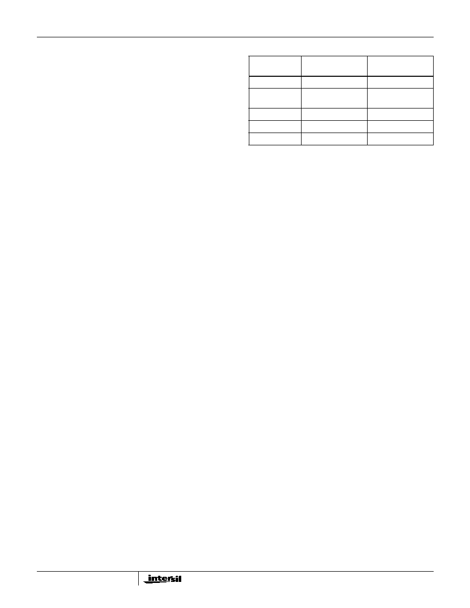
Optimum Feedback Resistor
The enclosed frequency response graphs detail the
performance of the HFA1150 in various gains. Although the
bandwidth dependency on A
CL
isn't as severe as that of a
voltage feedback amplifier, there is an appreciable decrease
in bandwidth at higher gains. This decrease can be
minimized by taking advantage of the current feedback
amplifier's unique relationship between bandwidth and R
F
.
All current feedback amplifiers require a feedback resistor,
even for unity gain applications, and the R
F
, in conjunction
with the internal compensation capacitor, sets the dominant
pole of the frequency response. Thus, the amplifier's
bandwidth is inversely proportional to R
F
. The HFA1150 is
optimized for a R
F
= 576
/499
(SOIC/SOT-23), at a gain of
+2. Decreasing R
F
decreases stability, resulting in excessive
peaking and overshoot (Note: Capacitive feedback causes
the same problems due to the feedback impedance
decrease at higher frequencies). At higher gains the
amplifier is more stable, so R
F
can be decreased in a trade-
off of stability for bandwidth. The table below lists
recommended R
F
values for various gains, and the expected
bandwidth.
5V Single Supply Operation
This amplifier operates at single supply voltages down to
4.5V. The dramatic supply current reduction at this operating
condition (refer also to Figure 25) makes this op amp an
even better choice for low power 5V systems. Refer to
Application Note AN9891 for further information.
Driving Capacitive Loads
Capacitive loads, such as an A/D input, or an improperly
terminated transmission line will degrade the amplifier's
phase margin resulting in frequency response peaking and
possible oscillations. In most cases, the oscillation can be
avoided by placing a resistor (R
S
) in series with the output
prior to the capacitance.
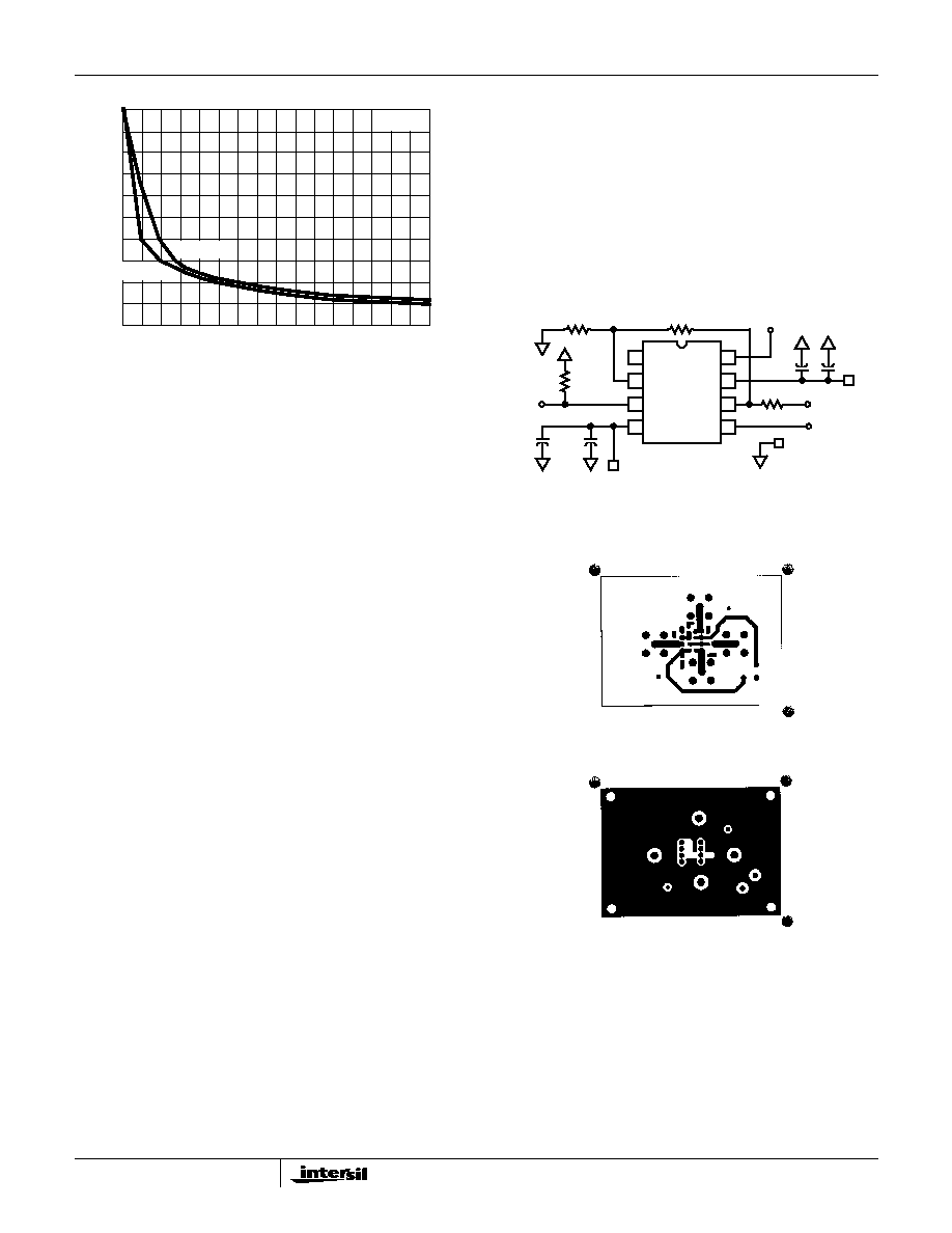
Figure 1 details starting points for the selection of this
resistor. The points on the curve indicate the R
S
and C
L
combinations for the optimum bandwidth, stability, and
settling time, but experimental fine tuning is recommended.
Picking a point above or to the right of the curve yields an
overdamped response, while points below or left of the curve
indicate areas of underdamped performance.
R
S
and C
L
form a low pass network at the output, thus
limiting system bandwidth well below the amplifier bandwidth
of 700MHz/540MHz (SOIC/SOT-23, A
V
= +2). By decreasing
R
S
as C
L
increases (as illustrated by the curves), the
maximum bandwidth is obtained without sacrificing stability.
In spite of this, bandwidth still decreases as the load
capacitance increases. For example, at A
V
= +2, R
S
= 20
,
C
L
= 22pF, the SOIC bandwidth is 410MHz, but the
bandwidth drops to 110MHz at A
V
= +2, R
S
= 5
,
C
L
= 390pF.
OPTIMUM FEEDBACK RESISTOR
A
CL
R
F
(
)
SOIC/SOT-23
BANDWIDTH (MHz)
SOIC/SOT-23
-1
422/464
650/540
+1
383, (+R
S
= 226)/
549, (+R
S
= 100)
600/500
+2
576/499
700/540
+5
348/422
480/400
+10
178/348
380/300
HFA1150
5
PC Board Layout
The frequency response of this amplifier depends greatly on
the amount of care taken in designing the PC board. The
use of low inductance components such as chip
resistors and chip capacitors is strongly recommended,
while a solid ground plane is a must!
Attention should be given to decoupling the power supplies.
A large value (10
µ
F) tantalum in parallel with a small value
chip (0.1
µ
F) capacitor works well in most cases.
Terminated microstrip signal lines are recommended at the
input and output of the device. Output capacitance, such as
that resulting from an improperly terminated transmission
line, will degrade the frequency response of the amplifier
and may cause oscillations. In most cases, the oscillation
can be avoided by placing a resistor in series with the output.
Care must also be taken to minimize the capacitance to ground
seen by the amplifier's inverting input. The larger this
capacitance, the worse the gain peaking, resulting in pulse
overshoot and eventual instability. To reduce this capacitance,
remove the ground plane under traces connected to -IN and
keep these traces as short as possible.
Examples of good high frequency layouts are the evaluation
boards shown below.
Evaluation Boards
The performance of the HFA1150IB (SOIC) may be
evaluated using the HFA11XX Evaluation Board and a SOIC
to DIP adaptor like the Aries Electronics Part Number
08-350000-10. The SOT-23 version can be evaluated using
the OPAMPSOT23EVAL board.
To order evaluation boards (part number HFA11XXEVAL or
OPAMPSOT23EVAL), please contact your local sales office.
The schematic and layout of the HFA11XXEVAL and
OPAMPSOT23EVAL boards are shown below.
HFA11XXEVAL TOP LAYOUT
HFA11XXEVAL BOTTOM LAYOUT
0
100
200
300
400
0
10
20
30
40
50
LOAD CAPACITANCE (pF)
SERIES OUTPUT RESIST
ANCE (
)
150
250
350
50
FIGURE 1. RECOMMENDED SERIES OUTPUT RESISTOR vs
LOAD CAPACITANCE
A
V
= +2
SOT-23
SOIC
FIGURE 2. HFA11XXEVAL SCHEMATIC
1
2
3
4
8
7
6
5
+5V
10
µ
F
0.1
µ
F
NC
50
GND
GND
511
511
-5V
0.1
µ
F
10
µ
F
50
IN
OUT
NC
V
H
+IN
V
L
V+
GND
1
V-
HFA1150