
3-1
TM
File Number
3076.10
CAUTION: These devices are sensitive to electrostatic discharge; follow proper IC Handling Procedures.
1-888-INTERSIL or 321-724-7143
|
Intersil and Design is a trademark of Intersil Corporation.
|
Copyright
©
Intersil Corporation 2000
HFA3046, HFA3096,
HFA3127, HFA3128
Ultra High Frequency Transistor Arrays
The HFA3046, HFA3096, HFA3127 and the HFA3128 are
Ultra High Frequency Transistor Arrays that are fabricated
from Intersil Corporation's complementary bipolar UHF-1
process. Each array consists of five dielectrically isolated
transistors on a common monolithic substrate. The NPN
transistors exhibit a f
T
of 8GHz while the PNP transistors
provide a f
T
of 5.5GHz. Both types exhibit low noise (3.5dB),
making them ideal for high frequency amplifier and mixer
applications.
The HFA3046 and HFA3127 are all NPN arrays while the
HFA3128 has all PNP transistors. The HFA3096 is an NPN-
PNP combination. Access is provided to each of the
terminals for the individual transistors for maximum
application flexibility. Monolithic construction of these
transistor arrays provides close electrical and thermal
matching of the five transistors.
For PSPICE models, please request AnswerFAX document
number 663046. Intersil also provides an Application Note
illustrating the use of these devices as RF amplifiers
(request AnswerFAX document 99315).
Features
∑ NPN Transistor (f
T
) . . . . . . . . . . . . . . . . . . . . . . . . . . 8GHz
∑ NPN Current Gain (h
FE
). . . . . . . . . . . . . . . . . . . . . . . 130
∑ NPN Early Voltage (V
A
) . . . . . . . . . . . . . . . . . . . . . . . 50V
∑ PNP Transistor (f
T
) . . . . . . . . . . . . . . . . . . . . . . . . 5.5GHz
∑ PNP Current Gain (h
FE
) . . . . . . . . . . . . . . . . . . . . . . . . 60
∑ PNP Early Voltage (V
A
) . . . . . . . . . . . . . . . . . . . . . . . 20V
∑ Noise Figure (50
) at 1.0GHz . . . . . . . . . . . . . . . . . 3.5dB
∑ Collector to Collector Leakage . . . . . . . . . . . . . . . . . <1pA
∑ Complete Isolation Between Transistors
∑ Pin Compatible with Industry Standard 3XXX Series
Arrays
Applications
∑ VHF/UHF Amplifiers
∑ VHF/UHF Mixers
∑ IF Converters
∑ Synchronous Detectors
Ordering Information
PART NUMBER
TEMP.
RANGE (
o
C)
PACKAGE
PKG.
NO.
HFA3046B
-55 to 125
14 Ld SOIC
M14.15
HFA3096B
-55 to 125
16 Ld SOIC
M16.15
HFA3127B
-55 to 125
16 Ld SOIC
M16.15
HFA3128B
-55 to 125
16 Ld SOIC
M16.15
Pinouts
HFA3046
TOP VIEW
HFA3096
TOP VIEW
HFA3127
TOP VIEW
HFA3128
TOP VIEW
1
2
3
4
5
6
7
14
13
12
11
10
9
8
Q
1
Q
2
Q
3
Q
4
Q
5
14
15
16
9
13
12
11
10
1
2
3
4
5
7
6
8
Q
1
NC
Q
3
Q
4
Q
2
Q
5
14
15
16
9
13
12
11
10
1
2
3
4
5
7
6
8
Q
1
Q
2
Q
3
Q
4
NC
Q
5
14
15
16
9
13
12
11
10
1
2
3
4
5
7
6
8
Q
1
Q
2
Q
3
Q
4
NC
Q
5
Data Sheet
October 1998

3-2
Absolute Maximum Ratings
Thermal Information
Collector to Emitter Voltage (Open Base) . . . . . . . . . . . . . . . . . . 8V
Collector to Base Voltage (Open Emitter) . . . . . . . . . . . . . . . . . 12V
Emitter to Base Voltage (Reverse Bias) . . . . . . . . . . . . . . . . . . . 5.5V
Collector Current (100% Duty Cycle) . . . . . 18.5mA at T
J
= 150
o
C
34mA at T
J
= 125
o
C
37mA at T
J
= 110
o
C
Peak Collector Current (Any Condition) . . . . . . . . . . . . . . . . . . 65mA
Operating Information
Temperature Range . . . . . . . . . . . . . . . . . . . . . . . . . -55
o
C to 125
o
C
Thermal Resistance (Typical, Note 1)
JA
(
o
C/W)
14 Ld SOIC Package . . . . . . . . . . . . . . . . . . . . . . . .
120
16 Ld SOIC Package . . . . . . . . . . . . . . . . . . . . . . . .
115
Maximum Power Dissipation (Any One Transistor) . . . . . . . . 0.15W
Maximum Junction Temperature (Die) . . . . . . . . . . . . . . . . . . . 175
o
C
Maximum Junction Temperature (Plastic Package) . . . . . . . 150
o
C
Maximum Storage Temperature Range . . . . . . . . . . -65
o
C to 150
o
C
Maximum Lead Temperature (Soldering 10s) . . . . . . . . . . . . 300
o
C
(SOIC - Lead Tips Only)
CAUTION: Stresses above those listed in "Absolute Maximum Ratings" may cause permanent damage to the device. This is a stress only rating and operation of the
device at these or any other conditions above those indicated in the operational sections of this specification is not implied.
NOTE:
1.
JA
is measured with the component mounted on an evaluation PC board in free air.
Electrical Specifications
T
A
= 25
o
C
PARAMETER
TEST CONDITIONS
DIE
SOIC
UNITS
MIN
TYP
MAX
MIN
TYP
MAX
DC NPN CHARACTERISTICS
Collector to Base Breakdown
Voltage, V
(BR)CBO
I
C
= 100
µ
A, I
E
= 0
12
18
-
12
18
-
V
Collector to Emitter Breakdown
Voltage, V
(BR)CEO
I
C
= 100
µ
A, I
B
= 0
8
12
-
8
12
-
V
Collector to Emitter Breakdown
Voltage, V
(BR)CES
I
C
= 100
µ
A, Base Shorted to Emitter
10
20
-
10
20
-
V
Emitter to Base Breakdown
Voltage, V
(BR)EBO
I
E
= 10
µ
A, I
C
= 0
5.5
6
-
5.5
6
-
V
Collector-Cutoff-Current, I
CEO
V
CE
= 6V, I
B
= 0
-
2
100
-
2
100
nA
Collector-Cutoff-Current, I
CBO
V
CB
= 8V, I
E
= 0
-
0.1
10
-
0.1
10
nA
Collector to Emitter Saturation
Voltage, V
CE(SAT)
I
C
= 10mA, I
B
= 1mA
-
0.3
0.5
-
0.3
0.5
V
Base to Emitter Voltage, V
BE
I
C
= 10mA
-
0.85
0.95
-
0.85
0.95
V
DC Forward-Current Transfer
Ratio, h
FE
I
C
= 10mA, V
CE
= 2V
40
130
-
40
130
-
Early Voltage, V
A
I
C
= 1mA, V
CE
= 3.5V
20
50
-
20
50
-
V
Base to Emitter Voltage Drift
I
C
= 10mA
-
-1.5
-
-
-1.5
-
mV/
o
C
Collector to Collector Leakage
-
1
-
-
1
-
pA
Electrical Specifications
T
A
= 25
o
C
PARAMETER
TEST CONDITIONS
DIE
SOIC
UNITS
MIN
TYP
MAX
MIN
TYP
MAX
DYNAMIC NPN CHARACTERISTICS
Noise Figure
f = 1.0GHz, V
CE
= 5V,
I
C
= 5mA, Z
S
= 50
-
3.5
-
-
3.5
-
dB
f
T
Current Gain-Bandwidth
Product
I
C
= 1mA, V
CE
= 5V
-
5.5
-
-
5.5
-
GHz
I
C
= 10mA, V
CE
= 5V
-
8
-
-
8
-
GHz
Power Gain-Bandwidth Product,
f
MAX
I
C
= 10mA, V
CE
= 5V
-
6
-
-
2.5
-
GHz
HFA3046, HFA3096, HFA3127, HFA3128

3-3
Base to Emitter Capacitance
V
BE
= -3V
-
200
-
-
500
-
fF
Collector to Base Capacitance
V
CB
= 3V
-
200
-
-
500
-
fF
Electrical Specifications
T
A
= 25
o
C (Continued)
PARAMETER
TEST CONDITIONS
DIE
SOIC
UNITS
MIN
TYP
MAX
MIN
TYP
MAX
Electrical Specifications
T
A
= 25
o
C
PARAMETER
TEST CONDITIONS
DIE
SOIC
UNITS
MIN
TYP
MAX
MIN
TYP
MAX
DC PNP CHARACTERISTICS
Collector to Base Breakdown
Voltage, V
(BR)CBO
I
C
= -100
µ
A, I
E
= 0
10
15
-
10
15
-
V
Collector to Emitter Breakdown
Voltage, V
(BR)CEO
I
C
= -100
µ
A, I
B
= 0
8
15
-
8
15
-
V
Collector to Emitter Breakdown
Voltage, V
(BR)CES
I
C
= -100
µ
A, Base Shorted to Emitter
10
15
-
10
15
-
V
Emitter to Base Breakdown
Voltage, V
(BR)EBO
I
E
= -10
µ
A, I
C
= 0
4.5
5
-
4.5
5
-
V
Collector Cutoff Current, I
CEO
V
CE
= -6V, I
B
= 0
-
2
100
-
2
100
nA
Collector Cutoff Current, I
CBO
V
CB
= -8V, I
E
= 0
-
0.1
10
-
0.1
10
nA
Collector to Emitter Saturation
Voltage, V
CE(SAT)
I
C
= -10mA, I
B
= -1mA
-
0.3
0.5
-
0.3
0.5
V
Base to Emitter Voltage, V
BE
I
C
= -10mA
-
0.85
0.95
-
0.85
0.95
V
DC Forward-Current Transfer
Ratio, h
FE
I
C
= -10mA, V
CE
= -2V
20
60
-
20
60
-
Early Voltage, V
A
I
C
= -1mA, V
CE
= -3.5V
10
20
-
10
20
-
V
Base to Emitter Voltage Drift
I
C
= -10mA
-
-1.5
-
-
-1.5
-
mV/
o
C
Collector to Collector Leakage
-
1
-
-
1
-
pA
Electrical Specifications
T
A
= 25
o
C
PARAMETER
TEST CONDITIONS
DIE
SOIC
UNITS
MIN
TYP
MAX
MIN
TYP
MAX
DYNAMIC PNP CHARACTERISTICS
Noise Figure
f = 1.0GHz, V
CE
= -5V,
I
C
= -5mA, Z
S
= 50
-
3.5
-
-
3.5
-
dB
f
T
Current Gain-Bandwidth
Product
I
C
= -1mA, V
CE
= -5V
-
2
-
-
2
-
GHz
I
C
= -10mA, V
CE
= -5V
-
5.5
-
-
5.5
-
GHz
Power Gain-Bandwidth
Product
I
C
= -10mA, V
CE
= -5V
-
3
-
-
2
-
GHz
Base to Emitter Capacitance
V
BE
= 3V
-
200
-
-
500
-
fF
Collector to Base Capacitance
V
CB
= -3V
-
300
-
-
600
-
fF
HFA3046, HFA3096, HFA3127, HFA3128
3-4
DIFFERENTIAL PAIR MATCHING CHARACTERISTICS FOR THE HFA3046
Input Offset Voltage
I
C
= 10mA, V
CE
= 5V
-
1.5
5.0
-
1.5
5.0
mV
Input Offset Current
I
C
= 10mA, V
CE
= 5V
-
5
25
-
5
25
µ
A
Input Offset Voltage TC
I
C
= 10mA, V
CE
= 5V
-
0.5
-
-
0.5
-
µ
V/
o
C
S-Parameter and PSPICE model data is available from Intersil Sales Offices, and Intersil Corporation's web site.
Electrical Specifications
T
A
= 25
o
C (Continued)
PARAMETER
TEST CONDITIONS
DIE
SOIC
UNITS
MIN
TYP
MAX
MIN
TYP
MAX
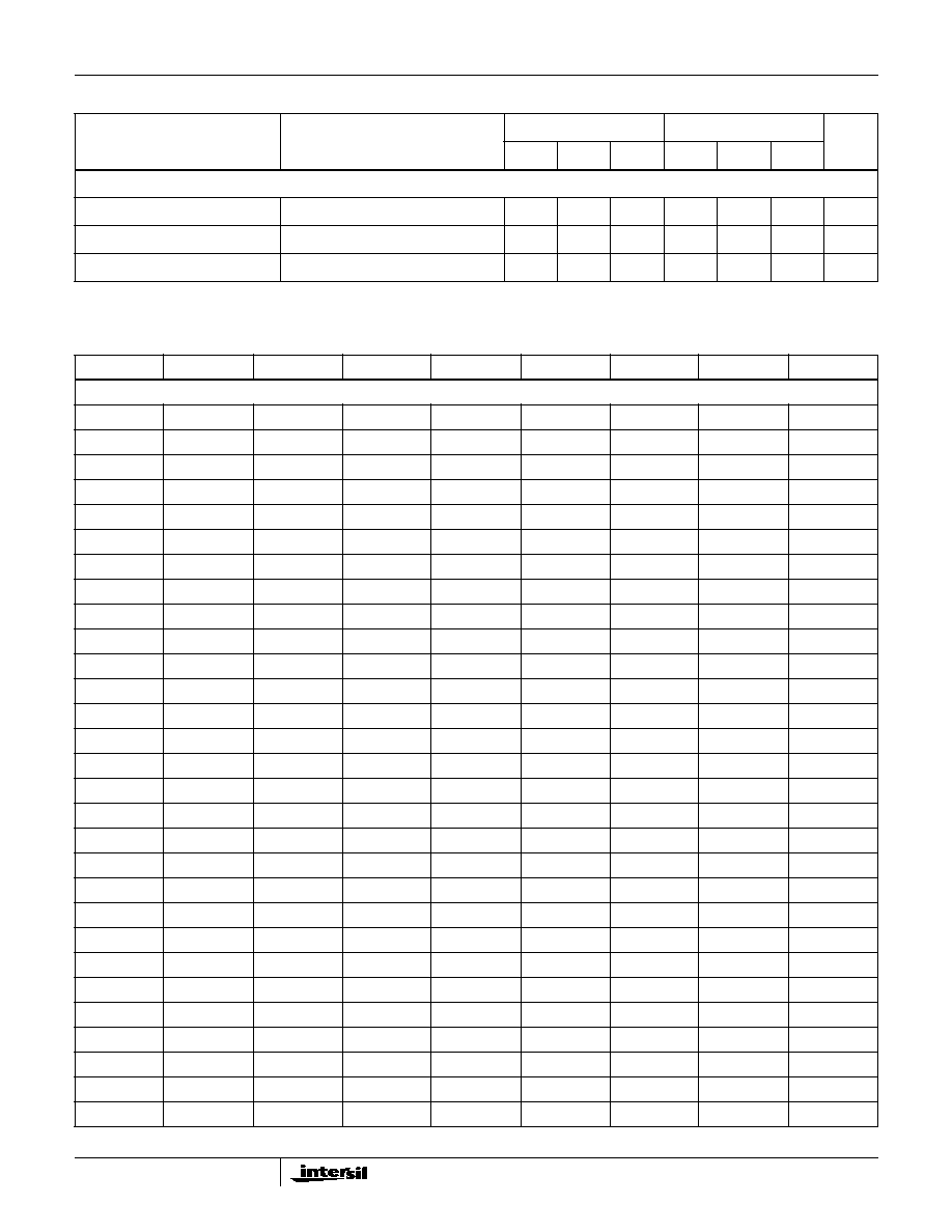
Common Emitter S-Parameters of NPN 3
µ
m x 50
µ
m Transistor
FREQ. (Hz)
|S
11
|
PHASE(S
11
)
|S
21
|
PHASE(S
21
)
|S
12
|
PHASE(S
12
)
|S
22
|
PHASE(S
22
)
V
CE
= 5V and I
C
= 5mA
1.0E+08
0.83
-11.78
11.07
168.57
1.41E-02
78.88
0.97
-11.05
2.0E+08
0.79
-22.82
10.51
157.89
2.69E-02
68.63
0.93
-21.35
3.0E+08
0.73
-32.64
9.75
148.44
3.75E-02
59.58
0.86
-30.44
4.0E+08
0.67
-41.08
8.91
140.36
4.57E-02
51.90
0.79
-38.16
5.0E+08
0.61
-48.23
8.10
133.56
5.19E-02
45.50
0.73
-44.59
6.0E+08
0.55
-54.27
7.35
127.88
5.65E-02
40.21
0.67
-49.93
7.0E+08
0.50
-59.41
6.69
123.10
6.00E-02
35.82
0.62
-54.37
8.0E+08
0.46
-63.81
6.11
119.04
6.27E-02
32.15
0.57
-58.10
9.0E+08
0.42
-67.63
5.61
115.57
6.47E-02
29.07
0.53
-61.25
1.0E+09
0.39
-70.98
5.17
112.55
6.63E-02
26.45
0.50
-63.96
1.1E+09
0.36
-73.95
4.79
109.91
6.75E-02
24.19
0.47
-66.31
1.2E+09
0.34
-76.62
4.45
107.57
6.85E-02
22.24
0.45
-68.37
1.3E+09
0.32
-79.04
4.15
105.47
6.93E-02
20.53
0.43
-70.19
1.4E+09
0.30
-81.25
3.89
103.57
7.00E-02
19.02
0.41
-71.83
1.5E+09
0.28
-83.28
3.66
101.84
7.05E-02
17.69
0.40
-73.31
1.6E+09
0.27
-85.17
3.45
100.26
7.10E-02
16.49
0.39
-74.66
1.7E+09
0.25
-86.92
3.27
98.79
7.13E-02
15.41
0.38
-75.90
1.8E+09
0.24
-88.57
3.10
97.43
7.17E-02
14.43
0.37
-77.05
1.9E+09
0.23
-90.12
2.94
96.15
7.19E-02
13.54
0.36
-78.12
2.0E+09
0.22
-91.59
2.80
94.95
7.21E-02
12.73
0.35
-79.13
2.1E+09
0.21
-92.98
2.68
93.81
7.23E-02
11.98
0.35
-80.09
2.2E+09
0.20
-94.30
2.56
92.73
7.25E-02
11.29
0.34
-80.99
2.3E+09
0.20
-95.57
2.45
91.70
7.27E-02
10.64
0.34
-81.85
2.4E+09
0.19
-96.78
2.35
90.72
7.28E-02
10.05
0.33
-82.68
2.5E+09
0.18
-97.93
2.26
89.78
7.29E-02
9.49
0.33
-83.47
2.6E+09
0.18
-99.05
2.18
88.87
7.30E-02
8.96
0.33
-84.23
2.7E+09
0.17
-100.12
2.10
88.00
7.31E-02
8.47
0.33
-84.97
2.8E+09
0.17
-101.15
2.02
87.15
7.31E-02
8.01
0.33
-85.68
2.9E+09
0.16
-102.15
1.96
86.33
7.32E-02
7.57
0.33
-86.37
HFA3046, HFA3096, HFA3127, HFA3128

3-5
3.0E+09
0.16
-103.11
1.89
85.54
7.32E-02
7.16
0.33
-87.05
V
CE
= 5V and I
C
= 10mA
1.0E+08
0.72
-16.43
15.12
165.22
1.27E-02
75.41
0.95
-14.26
2.0E+08
0.67
-31.26
13.90
152.04
2.34E-02
62.89
0.88
-26.95
3.0E+08
0.60
-43.76
12.39
141.18
3.13E-02
52.58
0.79
-37.31
4.0E+08
0.53
-54.00
10.92
132.57
3.68E-02
44.50
0.70
-45.45
5.0E+08
0.47
-62.38
9.62
125.78
4.05E-02
38.23
0.63
-51.77
6.0E+08
0.42
-69.35
8.53
120.37
4.31E-02
33.34
0.57
-56.72
7.0E+08
0.37
-75.26
7.62
116.00
4.49E-02
29.47
0.51
-60.65
8.0E+08
0.34
-80.36
6.86
112.39
4.63E-02
26.37
0.47
-63.85
9.0E+08
0.31
-84.84
6.22
109.36
4.72E-02
23.84
0.44
-66.49
1.0E+09
0.29
-88.83
5.69
106.77
4.80E-02
21.75
0.41
-68.71
1.1E+09
0.27
-92.44
5.23
104.51
4.86E-02
20.00
0.39
-70.62
1.2E+09
0.25
-95.73
4.83
102.53
4.90E-02
18.52
0.37
-72.28
1.3E+09
0.24
-98.75
4.49
100.75
4.94E-02
17.25
0.35
-73.76
1.4E+09
0.22
-101.55
4.19
99.16
4.97E-02
16.15
0.34
-75.08
1.5E+09
0.21
-104.15
3.93
97.70
4.99E-02
15.19
0.33
-76.28
1.6E+09
0.20
-106.57
3.70
96.36
5.01E-02
14.34
0.32
-77.38
1.7E+09
0.20
-108.85
3.49
95.12
5.03E-02
13.60
0.31
-78.41
1.8E+09
0.19
-110.98
3.30
93.96
5.05E-02
12.94
0.31
-79.37
1.9E+09
0.18
-113.00
3.13
92.87
5.06E-02
12.34
0.30
-80.27
2.0E+09
0.18
-114.90
2.98
91.85
5.07E-02
11.81
0.30
-81.13
2.1E+09
0.17
-116.69
2.84
90.87
5.08E-02
11.33
0.30
-81.95
2.2E+09
0.17
-118.39
2.72
89.94
5.09E-02
10.89
0.29
-82.74
2.3E+09
0.16
-120.01
2.60
89.06
5.10E-02
10.50
0.29
-83.50
2.4E+09
0.16
-121.54
2.49
88.21
5.11E-02
10.13
0.29
-84.24
2.5E+09
0.16
-122.99
2.39
87.39
5.12E-02
9.80
0.29
-84.95
2.6E+09
0.15
-124.37
2.30
86.60
5.12E-02
9.49
0.29
-85.64
2.7E+09
0.15
-125.69
2.22
85.83
5.13E-02
9.21
0.29
-86.32
2.8E+09
0.15
-126.94
2.14
85.09
5.13E-02
8.95
0.29
-86.98
2.9E+09
0.15
-128.14
2.06
84.36
5.14E-02
8.71
0.29
-87.62
3.0E+09
0.14
-129.27
1.99
83.66
5.15E-02
8.49
0.29
-88.25
Common Emitter S-Parameters of PNP 3
µ
m x 50
µ
m Transistor
FREQ. (Hz)
|S
11
|
PHASE(S
11
)
|S
21
|
PHASE(S
21
)
|S
12
|
PHASE(S
12
)
|S
22
|
PHASE(S
22
)
V
CE
= -5V and I
C
= -5mA
1.0E+08
0.72
-16.65
10.11
166.77
1.66E-02
77.18
0.96
-10.76
2.0E+08
0.68
-32.12
9.44
154.69
3.10E-02
65.94
0.90
-20.38
3.0E+08
0.62
-45.73
8.57
144.40
4.23E-02
56.39
0.82
-28.25
4.0E+08
0.57
-57.39
7.68
135.95
5.05E-02
48.66
0.74
-34.31
Common Emitter S-Parameters of NPN 3
µ
m x 50
µ
m Transistor
(Continued)
FREQ. (Hz)
|S
11
|
PHASE(S
11
)
|S
21
|
PHASE(S
21
)
|S
12
|
PHASE(S
12
)
|S
22
|
PHASE(S
22
)
HFA3046, HFA3096, HFA3127, HFA3128