 | –≠–ª–µ–∫—Ç—Ä–æ–Ω–Ω—ã–π –∫–æ–º–ø–æ–Ω–µ–Ω—Ç: HFA3424 | –°–∫–∞—á–∞—Ç—å:  PDF PDF  ZIP ZIP |

2-7
HFA3424
2.4GHz - 2.5GHz Low Noise Amplifier
The Intersil 2.4GHz PRISMTM chip set is
a highly integrated five-chip solution for
RF modems employing Direct
Sequence Spread Spectrum (DSSS)
signaling. The HFA3424 2.4GHz -
2.5GHz low noise amplifier is an optional chip that can be
added to the five chips in the PRISMTM chip set. The
HFA3424 offers increased sensitivity for systems targeting
802.11 specifications. (See Figure 1, the Typical Application
Diagram.)
The Intersil HFA3424 PRISMTM is a high performance low
noise amplifier in a low cost SOIC 8 lead surface mount
plastic package. The HFA3424 employs a fully monolithic
design which eliminates the need for external tuning
networks. It can be biased using 3V or 5V supplies and has
an option for biasing at higher currents for increased
dynamic range.
The HFA3424 is ideally suited for use where low noise
figure, high gain, high dynamic range and low power
consumption required. Typical applications include receiver
front ends in the Wireless Local Area Network (WLAN) and
wireless data collection markets in the 2.4GHz Industrial,
Scientific and Medical (ISM) band, as well as standard gain
blocks, buffer amps, driver amps and IF amps in both fixed
and portable systems.
Features
∑ Low Noise Figure . . . . . . . . . . . . . . . . . . . . . . . . . . 1.90dB
∑ High Gain . . . . . . . . . . . . . . . . . . . . . . . . . . . . . . . . . .14dB
∑ Low Power Consumption . . . . . . . . . . . . . . 3V to 5V, 5mA
∑ High Dynamic Range
∑ DC Decoupled RF Input and Output
∑ No External RF Tuning Elements Necessary
∑ Low Cost SOIC 8 Lead Plastic Package
Applications
∑ Systems Targeting IEEE 802.11 Standard
∑ TDD Quadrature-Modulated Communication
Systems
∑ Wireless Local Area Networks
∑ PCMCIA Wireless Transceivers
∑ ISM Systems
∑ TDMA Packet Protocol Radios
∑ PCS/Wireless PBX
∑ Wireless Local Loop
Pinout
HFA3424
(SOIC)
TOP VIEW
Functional Block Diagram
TM
Ordering Information
PART NUMBER
TEMP.
RANGE (
o
C)
PACKAGE
PKG.
NO.
HFA3424IB
-40 to 85
8 Ld SOIC
M8.15
HFA3424IB96
-40 to 85
Tape and Reel
GND
V
BIAS
RF IN
GND
1
2
3
4
8
7
6
5
GND
V
DD
RF OUT
GND
V
DD
RF IN
LNA 1
RF OUT
EXTENDED
BIAS
Data Sheet
January 1997
File Number
4131.2
CAUTION: These devices are sensitive to electrostatic discharge; follow proper IC Handling Procedures.
http://www.intersil.com or 407-727-9207
|
Copyright
©
Intersil Corporation 1999
PRISMÆ is a registered trademark of Intersil Corporation. PRISM logo is a trademark of Intersil Corporation.

2-8
Typical Application Diagram
For additional information on the PRISMTM chip set, call
(407) 724-7800 to access Intersil' AnswerFAX system. When
prompted, key in the four-digit document number (File #) of
the datasheets you wish to receive.
The four-digit file numbers are shown in Typical Application
Diagram, and correspond to the appropriate circuit.
FIGURE 1. TYPICAL TRANSCEIVER AMPLIFIER APPLICATIONS CIRCUIT USING THE HFA3424
NOTE:
Required for systems targeting 802.11 specifications.
QUAD IF MODULATOR
RFPA
HFA3925
HFA3724
DSSS BASEBAND PROCESSOR
D
A
T
A
T
O
MA
C
CTRL
HSP3824
TUNE/SELECT
HFA3524
0
o
/90
o
VCO
A/D
A/D
MAC-PHY
INTERFACE
802.11
VCO
DUAL SYNTHESIZER
HFA3624
UP/DOWN
CONVERTER
A/D
(FILE# 4067)
(FILE# 4064)
(FILE# 4062)
(FILE# 4066)
(FILE# 4132)
PRISMTM CHIP SET FILE #4063
M
U
X
M
U
X
DPSK
DEMOD
DPSK
MOD.
DE-
SPREAD
SPREAD
Q
I
HFA3424
(NOTE)
(FILE# 4131)
CCA
RXI
RXQ
RSSI
TXI
TXQ
˜
2
HFA3424

2-9
Absolute Maximum Ratings
Thermal Information
Supply Voltage, V
DD
. . . . . . . . . . . . . . . . . . . . . . . . . . . . . . +10V
DC
Input Power . . . . . . . . . . . . . . . . . . . . . . . . . . . . . . . . . . . . . +17dBm
Supply Current (Note 1) . . . . . . . . . . . . . . . . . . . . . . . . . . . . . . 30mA
Operating Conditions
Temperature Range . . . . . . . . . . . . . . . . . . . . . . . . . . -40
o
C to 85
o
C
Thermal Resistance (Typical, Note 2)
JA
(
o
C/W)
SOIC Package . . . . . . . . . . . . . . . . . . . . . . . . . . . . .
165
Maximum Storage Temperature Range . . . . . . . . . . -65
o
C to 150
o
C
Maximum Lead Temperature (Soldering 10s) . . . . . . . . . . . . .300
o
C
(SOIC - Lead Tips Only)
CAUTION: Stresses above those listed in "Absolute Maximum Ratings" may cause permanent damage to the device. This is a stress only rating and operation of the
device at these or any other conditions above those indicated in the operational sections of this specification is not implied.
NOTES:
1. Only if Pin 2 is used to increase current.
2.
JA
is measured with the component mounted on an evaluation PC board in free air.
Electrical Specifications
T
A
= 25
o
C, Z
0
= 50
, V
DD
= +5V, P
IN
= -30dBm, f = 2.45GHz, V
BIAS
= Open Circuit
Unless Otherwise Specified
PARAMETER
MIN
TYP
MAX
UNITS
LNA Input Frequency Range
2.4
-
2.5
GHz
Gain
12
14
16
dB
Noise Figure
-
1.90
2.30
dB
Input VSWR
-
1.5:1
-
Output VSWR
-
1.5:1
-
Input Return Loss
-
-14.0
-
dB
Output Return Loss
-
-14.0
-
dB
Output 1dB Compression
-
3
-
dBm
Input IP
3
-
1
-
dBm
Reverse Isolation
-
30
-
dB
Supply Current at V
DD
= 5V
3
5
7
mA
Supply Range
2.7
-
5.5
V
Typical Performance Curves
FIGURE 2. GAIN vs FREQUENCY
FIGURE 3. NOISE FIGURE vs FREQUENCY
T
A
= 25
o
C
3V, 5mA
5V, 20mA
5V, 5mA
2.2
2.3
2.4
2.5
2.6
2.7
18
16
14
12
10
FREQUENCY (GHz)
GAIN (dB)
T
A
= 25
o
C
3V, 5mA
5V, 20mA
5V, 5mA
2.40
2.42
2.44
2.46
2.48
2.50
2.0
1.9
1.8
1.7
1.6
FREQUENCY (GHz)
N
O
I
S
E FI
G
URE
(
dB
)
HFA3424

2-10
FIGURE 4. VSWR vs FREQUENCY
FIGURE 5. INPUT IP
3
vs FREQUENCY
FIGURE 6. GAIN vs FREQUENCY
FIGURE 7. NOISE FIGURE vs FREQUENCY
Typical Performance Curves
(Continued)
OUTPUT
INPUT
2.2
2.3
2.4
2.5
2.6
2.7
3.0
2.5
2.0
1.5
1.0
FREQUENCY (GHz)
VSWR
5V, 5mA, T
A
= 25
o
C
T
A
= 25
o
C
5V, 20mA
5V, 5mA
2.40
2.42
2.44
2.46
2.48
2.50
4
2
0
-2
-4
FREQUENCY (GHz)
INPUT IP
3
(dBm)
3V, 5mA
5V, 5mA
-40
o
C
2.2
2.3
2.4
2.5
2.6
2.7
18
16
14
12
10
FREQUENCY (GHz)
GAIN (dB)
85
o
C
25
o
C
25
o
C
5V, 5mA
2.6
2.3
2.0
1.7
1.4
FREQUENCY (GHz)
NOISE FIGURE (dB)
85
o
C
-40
o
C
2.40
2.42
2.44
2.46
2.48
2.50
HFA3424
2-11
All Intersil semiconductor products are manufactured, assembled and tested under ISO9000 quality systems certification.
Intersil semiconductor products are sold by description only. Intersil Corporation reserves the right to make changes in circuit design and/or specifications at any time with-
out notice. Accordingly, the reader is cautioned to verify that data sheets are current before placing orders. Information furnished by Intersil is believed to be accurate and
reliable. However, no responsibility is assumed by Intersil or its subsidiaries for its use; nor for any infringements of patents or other rights of third parties which may result
from its use. No license is granted by implication or otherwise under any patent or patent rights of Intersil or its subsidiaries.
For information regarding Intersil Corporation and its products, see web site http://www.intersil.com
Sales Office Headquarters
NORTH AMERICA
Intersil Corporation
P. O. Box 883, Mail Stop 53-204
Melbourne, FL 32902
TEL: (407) 724-7000
FAX: (407) 724-7240
EUROPE
Intersil SA
Mercure Center
100, Rue de la Fusee
1130 Brussels, Belgium
TEL: (32) 2.724.2111
FAX: (32) 2.724.22.05
ASIA
Intersil (Taiwan) Ltd.
7F-6, No. 101 Fu Hsing North Road
Taipei, Taiwan
Republic of China
TEL: (886) 2 2716 9310
FAX: (886) 2 2715 3029
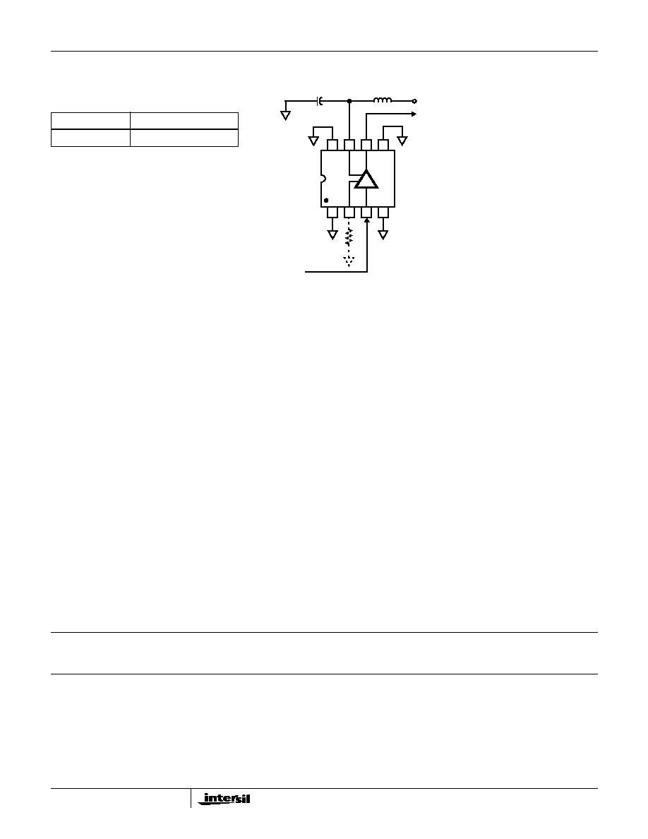
Typical Application Circuit
R
BB
1
2
3
4
8
7
6
5
+V
DD
RF SIGNAL OUTPUT 2.4GHz
15nH
(50
TRANSMISSION LINE)
500pF
PIN 2 ALLOWS FOR AN EXTERNAL RESISTOR
R
BB
TO BE USED TO GROUND FOR AN OPTIONAL
20mA CURRENT OPERATION. RECOMMENDED
VALUES FOR THE CHIP RESISTOR ARE 30
TO 35
.
V
BIAS
(PIN 2)
NORMAL BIAS
EXTENDED BIAS
Open
30
To 35
To Ground
SEE NOTE 2
RF SIGNAL INPUT 2.4GHz
(50
TRANSMISSION LINE)
SEE NOTE 2
NOTE:
3.
No DC blocking capacitor required on LNA input or output transmission lines.
FIGURE 8. REFERENCE APPLICATION/TEST DESIGN SETUP SCHEMATIC: LOW NOISE AMPLIFIER
HFA3424