
CAUTION: These devices are sensitive to electrostatic discharge. Users should follow proper ESD Handling Procedures.
Copyright
©
Harris Corporation 1995
3-98
Semiconductor
HGTG20N120E2
34A, 1200V N-Channel IGBT
Package
JEDEC STYLE TO-247
Terminal Diagram
COLLECTOR
GATE
COLLECTOR
EMITTER
(BOTTOM SIDE
METAL)
C
G
E
Features
∑ 34A, 1200V
∑ Latch Free Operation
∑ Typical Fall Time - 780ns
∑ High Input Impedance
∑ Low Conduction Loss
Description
The HGTG20N120E2 is a MOS gated, high voltage switch-
ing device combining the best features of MOSFETs and
bipolar transistors. The device has the high input impedance
of a MOSFET and the low on-state conduction loss of a
bipolar transistor. The much lower on-state voltage drop
varies only moderately between +25
o
C and +150
o
C.
IGBTs are ideal for many high voltage switching applications
operating at frequencies where low conduction losses are
essential, such as: AC and DC motor controls, power
supplies and drivers for solenoids, relays and contactors.
The development type number for this device is TA49009.
PACKAGING AVAILABILITY
PART NUMBER
PACKAGE
BRAND
HGTG20N120E2
TO-247
G20N120E2
April 1995
Absolute Maximum Ratings
T
C
= +25
o
C, Unless Otherwise Specified
HGTG20N120E2
UNITS
Collector-Emitter Breakdown Voltage. . . . . . . . . . . . . . . . . . . . . . . . . . . . . . . . . . . BV
CES
1200
V
Collector-Gate Breakdown Voltage R
GE
= 1M
. . . . . . . . . . . . . . . . . . . . . . . . . . . BV
CGR
1200
V
Collector Current Continuous
At T
C
= +25
o
C . . . . . . . . . . . . . . . . . . . . . . . . . . . . . . . . . . . . . . . . . . . . . . . . . . . . . I
C25
At T
C
= +90
o
C . . . . . . . . . . . . . . . . . . . . . . . . . . . . . . . . . . . . . . . . . . . . . . . . . . . . . I
C90
34
20
A
A
Collector Current Pulsed (Note 1) . . . . . . . . . . . . . . . . . . . . . . . . . . . . . . . . . . . . . . . . I
CM
100
A
Gate-Emitter Voltage Continuous. . . . . . . . . . . . . . . . . . . . . . . . . . . . . . . . . . . . . . . V
GES
±
20
V
Gate-Emitter Voltage Pulsed . . . . . . . . . . . . . . . . . . . . . . . . . . . . . . . . . . . . . . . . . . V
GEM
±
30
V
Switching SOA at T
C
= +150
o
C . . . . . . . . . . . . . . . . . . . . . . . . . . . . . . . . . . . . . . . .SSOA
100A at 0.8 BV
CES
-
Power Dissipation Total at T
C
= +25
o
C . . . . . . . . . . . . . . . . . . . . . . . . . . . . . . . . . . . . P
D
150
W
Power Dissipation Derating T
C
> +25
o
C . . . . . . . . . . . . . . . . . . . . . . . . . . . . . . . . . . . . . .
1.20
W/
o
C
Operating and Storage Junction Temperature . . . . . . . . . . . . . . . . . . . . . . . . . . . T
J
, T
STG
-55 to +150
o
C
Maximum Lead Temperature for Soldering . . . . . . . . . . . . . . . . . . . . . . . . . . . . . . . . . . T
L
(0.125" from case for 5 seconds)
260
o
C
Short Circuit Withstand Time (Note 2)
At V
GE
= 15V . . . . . . . . . . . . . . . . . . . . . . . . . . . . . . . . . . . . . . . . . . . . . . . . . . . . . . t
SC
At V
GE
= 10V . . . . . . . . . . . . . . . . . . . . . . . . . . . . . . . . . . . . . . . . . . . . . . . . . . . . . . t
SC
3
15
µ
s
µ
s
NOTES:
1. Repetitive Rating: Pulse width limited by maximum junction temperature.
2. V
CE(PEAK)
= 720V, T
C
= +125
o
C, R
GE
= 25
HARRIS SEMICONDUCTOR IGBT PRODUCT IS COVERED BY ONE OR MORE OF THE FOLLOWING U.S. PATENTS:
4,364,073
4,417,385
4,430,792
4,443,931
4,466,176
4,516,143
4,532,534
4,567,641
4,587,713
4,598,461
4,605,948
4,618,872
4,620,211
4,631,564
4,639,754
4,639,762
4,641,162
4,644,637
4,682,195
4,684,413
4,694,313
4,717,679
4,743,952
4,783,690
4,794,432
4,801,986
4,803,533
4,809,045
4,809,047
4,810,665
4,823,176
4,837,606
4,860,080
4,883,767
4,888,627
4,890,143
4,901,127
4,904,609
4,933,740
4,963,951
4,969,027
File Number
3370.2
3-99
Specifications HGTG20N120E2
Electrical Specifications
T
C
= +25
o
C, Unless Otherwise Specified
PARAMETERS
SYMBOL
TEST CONDITIONS
LIMITS
UNIT
MIN
TYP
MAX
Collector-Emitter Breakdown
Voltage
BV
CES
I
C
= 250
µ
A, V
GE
= 0V
1200
-
-
V
Collector-Emitter Leakage Current
I
CES
V
CE
= BV
CES
T
C
= +25
o
C
-
-
250
µ
A
V
CE
= 0.8 BV
CES
T
C
= +125
o
C
-
-
1.0
mA
Collector-Emitter Saturation
Voltage
V
CE(SAT)
I
C
= I
C90
, V
GE
= 15V
T
C
= +25
o
C
-
2.9
3.5
V
T
C
= +125
o
C
-
3.0
3.6
V
I
C
= I
C90
, V
GE
= 10V
T
C
= +25
o
C
-
3.1
3.8
V
T
C
= +125
o
C
-
3.3
4.0
V
Gate-Emitter Threshold Voltage
V
GE(TH)
I
C
= 500
µ
A,
V
CE
= V
GE
T
C
= +25
o
C
3.0
4.5
6.0
V
Gate-Emitter Leakage Current
I
GES
V
GE
=
±
20V
-
-
±
250
nA
Gate-Emitter Plateau Voltage
V
GEP
I
C
= I
C90
, V
CE
= 0.5 BV
CES
-
7.0
-
V
On-State Gate Charge
Q
G(ON)
I
C
= I
C90
,
V
CE
= 0.5 BV
CES
V
GE
= 15V
-
110
150
nC
V
GE
= 20V
-
150
200
nC
Current Turn-On Delay Time
t
D(ON)
R
L
= 48
I
C
= I
C90
, V
GE
= 15V,
V
CE
= 0.8 BV
CES
,
R
G
= 25
,
T
J
= +125
o
C
-
100
-
ns
Current Rise Time
t
R
-
150
-
ns
Current Turn-Off Delay Time
t
D(OFF)I
L = 50
µ
H
-
520
620
ns
Current Fall Time
t
FI
-
780
1000
ns
Turn-Off Energy (Note 1)
W
OFF
-
7.0
-
mJ
Current Turn-On Delay Time
t
D(ON)
R
L
= 48
I
C
= I
C90
, V
GE
= 10V,
V
CE
= 0.8 BV
CES
,
R
G
= 25
,
T
J
= +125
o
C
-
100
-
ns
Current Rise Time
t
R
-
150
-
ns
Current Turn-Off Delay Time
t
D(OFF)I
L = 50
µ
H
-
420
520
ns
Current Fall Time
t
FI
-
780
1000
ns
Turn-Off Energy (Note 1)
W
OFF
-
7.0
-
mJ
Thermal Resistance
R
JC
-
0.70
0.83
o
C/W
NOTE:
1. Turn-Off Energy Loss (W
OFF
) is defined as the integral of the instantaneous power loss starting at the trailing edge of the input pulse and
ending at the point where the collector current equals zero (I
CE
= 0A). The HGTG20N120E2 was tested per JEDEC standard No. 24-1
Method for Measurement of Power Device Turn-Off Switching Loss. This test method produces the true total Turn-Off Energy Loss.
3-100
HGTG20N120E2
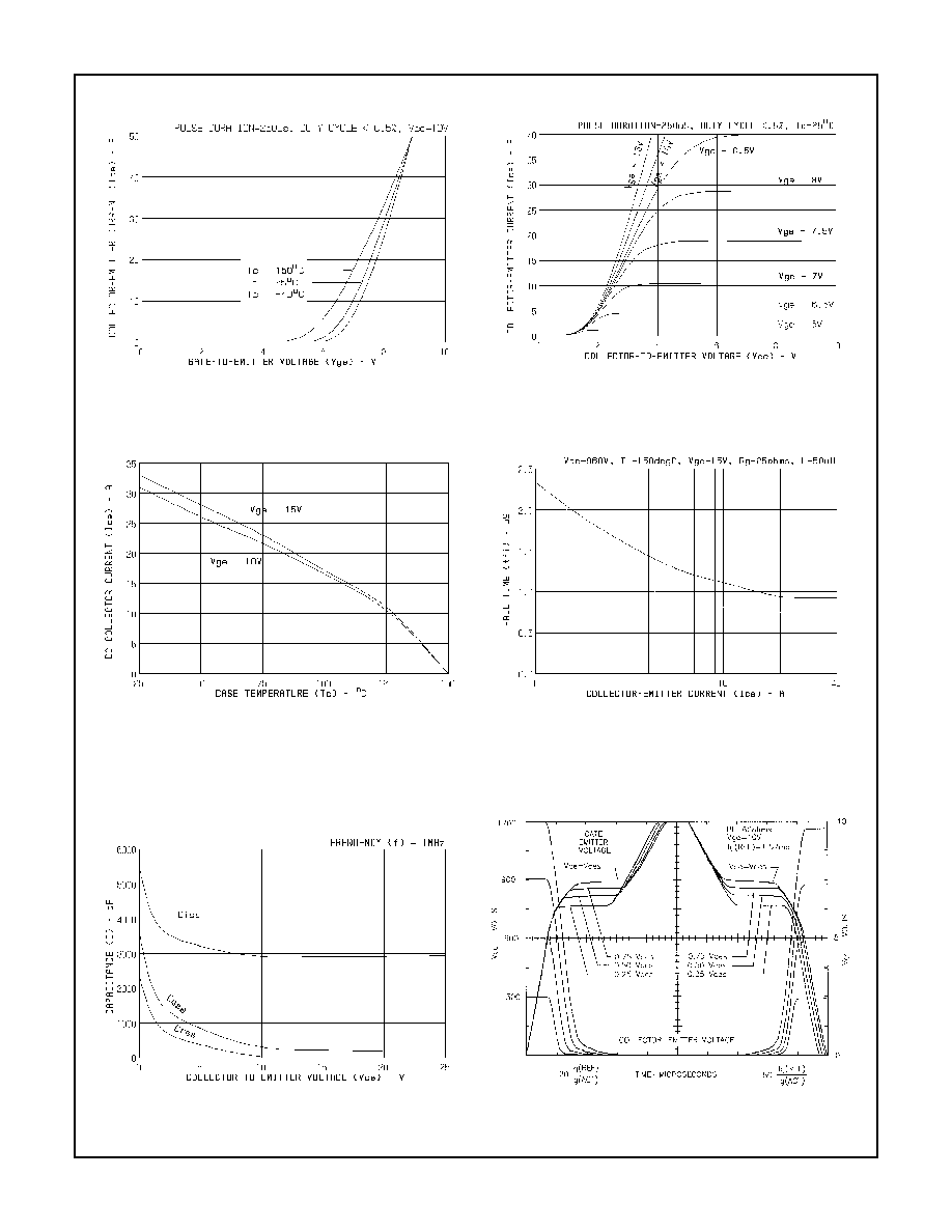
Typical Performance Curves
FIGURE 1. TRANSFER CHARACTERISTICS (TYPICAL)
FIGURE 2. SATURATION CHARACTERISTICS (TYPICAL)
FIGURE 3. MAXIMUM DC COLLECTOR CURRENT AS A
FUNCTION OF CASE TEMPERATURE
FIGURE 4. FALL TIME AS A FUNCTION OF COLLECTOR-
EMITTER CURRENT
FIGURE 5. CAPACITANCE AS A FUNCTION OF COLLECTOR-
EMITTER VOLTAGE
FIGURE 6. NORMALIZED SWITCHING WAVEFORMS AT
CONSTANT GATE CURRENT. (REFER TO
APPLICATION NOTES AN7254 AND AN7260)

3-101
HGTG20N120E2
FIGURE 7. SATURATION VOLTAGE AS A FUNCTION OF
COLLECTOR-EMITTER CURRENT
FIGURE 8. TURN-OFF SWITCHING LOSS AS A FUNCTION OF
COLLECTOR-EMITTER CURRENT
FIGURE 9. TURN-OFF DELAY AS A FUNCTION OF COLLECTOR-
EMITTER CURRENT
FIGURE 10. OPERATING FREQUENCY AS A FUNCTION OF
COLLECTOR-EMITTER CURRENT AND VOLTAGE
FIGURE 11. COLLECTOR-EMITTER SATURATION VOLTAGE
Typical Performance Curves
(Continued)
3-102
HGTG20N120E2
Handling Precautions for IGBTs
Insulated Gate Bipolar Transistors are susceptible to gate-
insulation damage by the electrostatic discharge of energy
through the devices. When handling these devices, care
should be exercised to assure that the static charge built in
the handler's body capacitance is not discharged through
the device. With proper handling and application procedures,
however, IGBTs are currently being extensively used in
production by numerous equipment manufacturers in
military, industrial and consumer applications, with virtually
no damage problems due to electrostatic discharge. IGBTs
can be handled safely if the following basic precautions are
taken:
1. Prior to assembly into a circuit, all leads should be kept
shorted together either by the use of metal shorting
springs or by the insertion into conductive material such
as "
ECCOSORBD LD26" or equivalent.
2. When devices are removed by hand from their carriers,
the hand being used should be grounded by any suitable
means - for example, with a metallic wristband.
3. Tips of soldering irons should be grounded.
4. Devices should never be inserted into or removed from
circuits with power on.
5. Gate Voltage Rating - Never exceed the gate-voltage
rating of VGEM. Exceeding the rated VGE can result in
permanent damage to the oxide layer in the gate region.
6. Gate Termination - The gates of these devices are
essentially capacitors. Circuits that leave the gate open-
circuited or floating should be avoided. These conditions
can result in turn-on of the device due to voltage buildup
on the input capacitor due to leakage currents or pickup.
7. Gate Protection - These devices do not have an internal
monolithic zener diode from gate to emitter. If gate
protection is required an external zener is recommended.
Trademark Emerson and Cumming, Inc.
Operating Frequency Information
Operating frequency information for a typical device (Figure
10) is presented as a guide for estimating device performance
for a specific application. Other typical frequency vs collector
current (I
CE
) plots are possible using the information shown
for a typical unit in Figures 7, 8 and 9. The operating
frequency plot (Figure 10) of a typical device shows f
MAX1
or
f
MAX2
whichever is smaller at each point. The information is
based on measurements of a typical device and is bounded
by the maximum rated junction temperature.
f
MAX1
is defined by f
MAX1
= 0.05/t
D(OFF)I
. t
D(OFF)I
deadtime
(the denominator) has been arbitrarily held to 10% of the on-
state time for a 50% duty factor. Other definitions are
possible. t
D(OFF)I
is defined as the time between the 90%
point of the trailing edge of the input pulse and the point
where the collector current falls to 90% of its maximum
value. Device turn-off delay can establish an additional fre-
quency limiting condition for an application other than T
JMAX
.
t
D(OFF)I
is important when controlling output ripple under a
lightly loaded condition. f
MAX2
is defined by f
MAX2
= (Pd - Pc)/
W
OFF
. The allowable dissipation (Pd) is defined by Pd =
(T
JMAX
- T
C
)/R
JC
. The sum of device switching and conduc-
tion losses must not exceed Pd. A 50% duty factor was used
(Figure 10) and the conduction losses (Pc) are approximated
by Pc = (V
CE
∑
I
CE
)/2. W
OFF
is defined as the integral of the
instantaneous power loss starting at the trailing edge of the
input pulse and ending at the point where the collector
current equals zero (I
CE
= 0A).
The switching power loss (Figure 10) is defined as f
MAX2
∑
W
OFF
. Turn-on switching losses are not included because
they can be greatly influenced by external circuit conditions
and components.
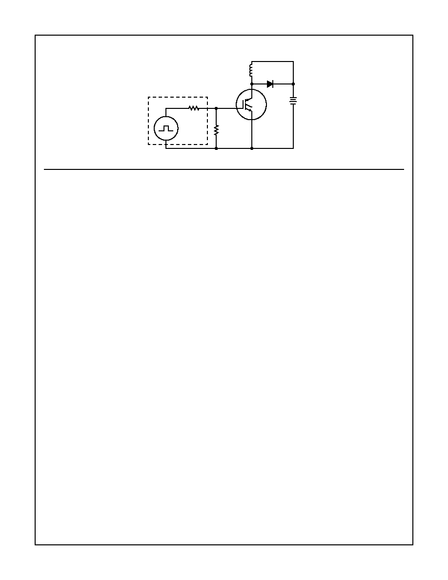
Test Circuit
FIGURE 12. INDUCTIVE SWITCHING TEST CIRCUIT
20V
0V
R
GEN
= 50
1/R
G
= 1/R
GEN
+ 1/R
GE
R
GE
= 50
L = 50
µ
H
V
CC
960V
+
-