3-103
CAUTION: These devices are sensitive to electrostatic discharge; follow proper IC Handling Procedures.
http://www.intersil.com or 407-727-9207
|
Copyright
©
Intersil Corporation 1999
HGTG24N60D1
24A, 600V N-Channel IGBT
Features
∑ 24A, 600V
∑ Latch Free Operation
∑ Typical Fall Time <500ns
∑ High Input Impedance
∑ Low Conduction Loss
Description
The IGBT is a MOS gated high voltage switching device
combining the best features of MOSFETs and bipolar
transistors. The device has the high input impedance of a
MOSFET and the low on-state conduction loss of a bipolar
transistor. The much lower on-state voltage drop varies only
moderately between +25
o
C and +150
o
C.
IGBTs are ideal for many high voltage switching applications
operating at moderate frequencies where low conduction losses
are essential, such as: AC and DC motor controls, power sup-
plies and drivers for solenoids, relays and contactors.
PACKAGING AVAILABILITY
PART NUMBER
PACKAGE
BRAND
HGTG24N60D1
TO-247
G24N60D1
May 1995
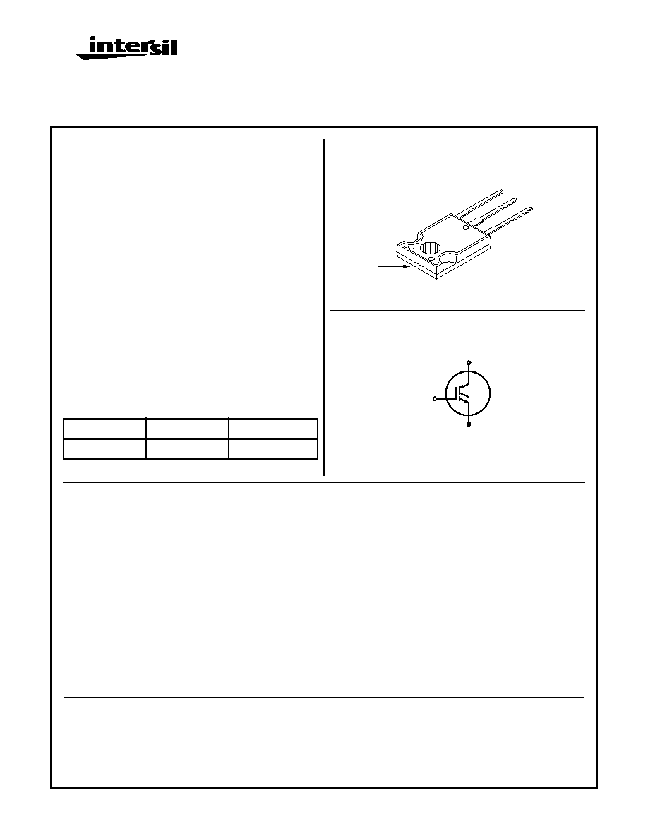
Package
JEDEC STYLE TO-247
Terminal Diagram
N-CHANNEL ENHANCEMENT MODE
COLLECTOR
GATE
COLLECTOR
EMITTER
(BOTTOM SIDE
METAL)
C
E
G
Absolute Maximum Ratings
T
C
= +25
o
C, Unless Otherwise Specific
HGTG24N60D1
UNITS
Collector-Emitter Voltage . . . . . . . . . . . . . . . . . . . . . . . . . . . . . . . . . . . . . . . . . . . . BV
CES
600
V
Collector-Gate Voltage R
GE
= 1M
. . . . . . . . . . . . . . . . . . . . . . . . . . . . . . . . . . . . BV
CGR
600
V
Collector Current Continuous at T
C
= +25
o
C . . . . . . . . . . . . . . . . . . . . . . . . . . . . . . . I
C25
40
A
at V
GE
= 15V at T
C
= +90
o
C . . . . . . . . . . . . . . . . . . . . I
C90
24
A
Collector Current Pulsed (Note 1) . . . . . . . . . . . . . . . . . . . . . . . . . . . . . . . . . . . . . . . . I
CM
96
A
Gate-Emitter Voltage Continuous. . . . . . . . . . . . . . . . . . . . . . . . . . . . . . . . . . . . . . . V
GES
±
25
V
Switching Safe Operating Area at T
J
= +150
o
C . . . . . . . . . . . . . . . . . . . . . . . . . . . .SSOA
60A at 0.8 BV
CES
-
Power Dissipation Total at T
C
= +25
o
C . . . . . . . . . . . . . . . . . . . . . . . . . . . . . . . . . . . . P
D
125
W
Power Dissipation Derating T
C
> +25
o
C . . . . . . . . . . . . . . . . . . . . . . . . . . . . . . . . . . . . . .
1.0
W/
o
C
Operating and Storage Junction Temperature Range . . . . . . . . . . . . . . . . . . . . . T
J
, T
STG
-55 to +150
o
C
Maximum Lead Temperature for Soldering . . . . . . . . . . . . . . . . . . . . . . . . . . . . . . . . . . T
L
260
o
C
(0.125 inch from case for 5s)
NOTE:
1. Repetitive Rating: Pulse width limited by maximum junction temperature.
INTERSIL CORPORATION IGBT PRODUCT IS COVERED BY ONE OR MORE OF THE FOLLOWING U.S. PATENTS:
4,364,073
4,417,385
4,430,792
4,443,931
4,466,176
4,516,143
4,532,534
4,567,641
4,587,713
4,598,461
4,605,948
4,618,872
4,620,211
4,631,564
4,639,754
4,639,762
4,641,162
4,644,637
4,682,195
4,684,413
4,694,313
4,717,679
4,743,952
4,783,690
4,794,432
4,801,986
4,803,533
4,809,045
4,809,047
4,810,665
4,823,176
4,837,606
4,860,080
4,883,767
4,888,627
4,890,143
4,901,127
4,904,609
4,933,740
4,963,951
4,969,027
File Number
2831.3
3-104
Specifications HGTG24N60D1
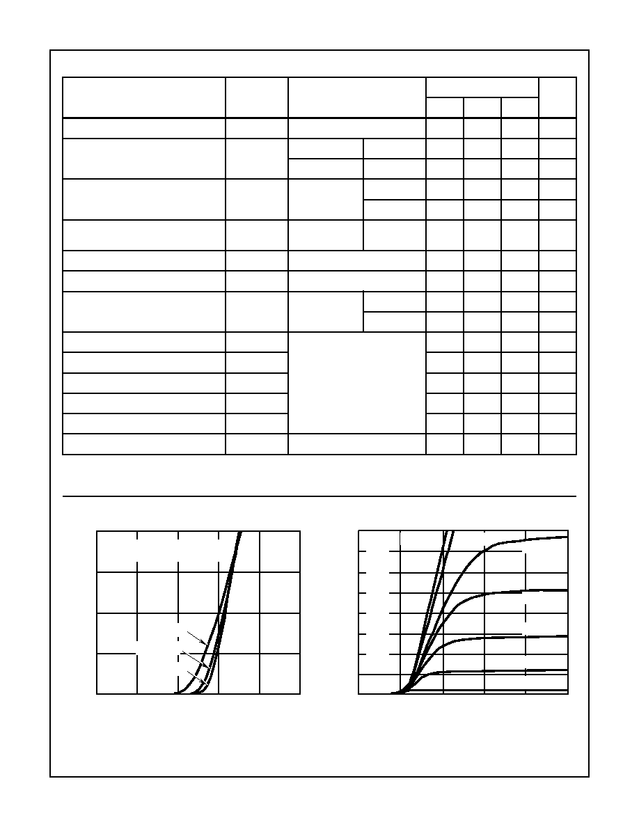
Electrical Specifications
T
C
= +25
o
C, Unless Otherwise Specified
PARAMETERS
SYMBOL
TEST CONDITIONS
LIMITS
UNITS
MIN
TYP
MAX
Collector-Emitter Breakdown Voltage
BV
CES
I
C
= 250
µ
A, V
GE
= 0V
600
-
-
V
Collector-Emitter Leakage Voltage
I
CES
V
CE
= BV
CES
T
C
= +25
o
C
-
-
1.0
mA
V
CE
= 0.8 BV
CES
T
C
= +125
o
C
-
-
4.0
mA
Collector-Emitter Saturation Voltage
V
CE(SAT)
I
C
= I
C90
,
V
GE
= 15V
T
C
= +25
o
C
-
1.7
2.3
V
T
C
= +125
o
C
-
1.9
2.5
V
Gate-Emitter Threshold Voltage
V
GE(TH)
I
C
= 250
µ
A,
V
CE
= V
GE
T
C
= +25
o
C
3.0
4.5
6.0
V
Gate-Emitter Leakage Current
I
GES
V
GE
=
±
20V
-
-
±
500
nA
Gate-Emitter Plateau Voltage
V
GEP
I
C
= I
C90
, V
CE
= 0.5 BV
CES
-
6.3
-
V
On-State Gate Charge
Q
G(ON)
I
C
= I
C90
,
V
CE
= 0.5 BV
CES
V
GE
= 15V
-
120
155
nC
V
GE
= 20V
-
155
200
nC
Current Turn-On Delay Time
t
D(ON)I
L = 500
µ
H, I
C
= I
C90
, R
G
= 25
,
V
GE
= 15V, T
J
= +150
o
C,
V
CE
= 0.8 BV
CES
-
100
-
ns
Current Rise Time
t
RI
-
150
-
ns
Current Turn-Off Delay Time
t
D(OFF)I
-
700
900
ns
Current Fall Time
t
FI
-
450
600
ns
Turn-Off Energy (Note 1)
W
OFF
-
4.3
-
mJ
Thermal Resistance
R
JC
-
-
1.00
o
C/W
NOTE: 1. Turn-Off Energy Loss (W
OFF
) is defined as the integral of the instantaneous power loss starting at the trailing edge of the input pulse and
ending at the point where the collector current equals zero (I
CE
= 0A) The HGTG24N60D1 was tested per JEDEC standard No. 24-1
Method for Measurement of Power Device Turn-Off Switching Loss. This test method produces the true total Turn-Off Energy Loss.
Typical Performance Curves
FIGURE 1. TRANSFER CHARACTERISTICS (TYPICAL)
FIGURE 2. SATURATION CHARACTERISTICS (TYPICAL)
40
30
20
10
0
I
CE
, COLLECT
OR-EMITTER CURRENT (A)
0
2
4
6
8
10
V
GE
, GATE-TO-EMITTER VOLTAGE (V)
PULSE DURATION = 250
µ
s
DUTY CYCLE < 0.5%, V
CE
= 15V
T
C
= +150
o
C
T
C
= +25
o
C
T
C
= -40
o
C
40
35
30
25
20
15
10
5
0
I
CE
, COLLECT
OR-EMITTER CURRENT (A)
0
1
2
3
4
5
V
CE
, COLLECTOR-TO-EMITTER VOLTAGE (V)
PULSE DURA
TION = 250
µ
s
DUTY CYCLE < 0.5%, T
C
= +25
o
C
V
GE
= 15V
V
GE
= 7.0V
V
GE
= 6.5V
V
GE
= 6.0V
V
GE
= 5.5V
V
GE
= 10V
V
GE
= 5.0V
3-105
HGTG24N60D1
FIGURE 3. DC COLLECTOR CURRENT vs CASE TEMPERATURE
FIGURE 4. FALL TIME vs COLLECTOR-EMITTER CURRENT
FIGURE 5. CAPACITANCE vs COLLECTOR-EMITTER VOLTAGE
FIGURE 6. NORMALIZED SWITCHING WAVEFORMS AT CON-
STANT GATE CURRENT (REFER TO APPLICATION
NOTES AN7254 AND AN7260)
FIGURE 7. SATURATION VOLTAGE vs COLLECTOR-EMITTER
CURRENT
FIGURE 8. TURN-OFF SWITCHING LOSS vs COLLECTOR-
EMITTER CURRENT
Typical Performance Curves
(Continued)
50
40
30
20
0
I
CE
, DC COLLECT
OR CURRENT (A)
+25
+50
+75
+100
+125
+150
T
C
, CASE TEMPERATURE (
o
C)
V
GE
= 15V
10
t
FI
, F
ALL TIME (ns)
1
10
40
I
CE
, COLLECTOR-EMITTER CURRENT (A)
V
CE
= 480V, V
GE
= 10V AND 15V,
T
J
= +150
o
C, R
G
= 25
, L = 500
µ
H
1000
900
800
700
600
500
400
300
200
100
0
6000
5000
4000
3000
2000
1000
0
C, CAP
ACIT
ANCE (pF)
0
5
10
15
20
25
V
CE
, COLLECTOR-TO-EMITTER VOLTAGE (V)
f = 1MHz
C
ISS
C
OSS
C
RSS
600
450
300
150
0
V
CE
, COLLECT
OR-EMITTER VOL
T
AGE (V)
V
GE
, GA
TE-EMITTER VOL
T
AGE (V)
10
5
0
20
I
G(REF)
I
G(ACT)
80
I
G(REF)
I
G(ACT)
TIME (
µ
s)
V
CC
= BV
CES
V
CC
= BV
CES
0.75 BV
CES
0.50 BV
CES
0.25 BV
CES
0.75 BV
CES
0.50 BV
CES
0.25 BV
CES
R
L
= 30
I
G(REF)
= 1.83mA
V
GE
= 10V
7.5
2.5
3
2
1
0
V
CE(ON)
, SA
TURA
TION VOL
T
AGE (V)
1
10
40
I
CE
, COLLECTOR-EMITTER CURRENT (A)
T
J
= +150
o
C
V
GE
= 10V
V
GE
= 15V
7.00
1.00
0.10
0.05
W
OFF
, TURN-OFF SWITCHING LOSS (mJ)
1
10
40
I
CE
, COLLECTOR-EMITTER CURRENT (A)
T
J
= +150
o
C, R
G
= 25
,
L = 500
µ
H
V
CE
= 480V, V
GE
= 10V, 15V
V
CE
= 240V, V
GE
= 10V, 15V
3-106
All Intersil semiconductor products are manufactured, assembled and tested under ISO9000 quality systems certification.
Intersil products are sold by description only. Intersil Corporation reserves the right to make changes in circuit design and/or specifications at any time without
notice. Accordingly, the reader is cautioned to verify that data sheets are current before placing orders. Information furnished by Intersil is believed to be accurate
and reliable. However, no responsibility is assumed by Intersil or its subsidiaries for its use; nor for any infringements of patents or other rights of third parties which
may result from its use. No license is granted by implication or otherwise under any patent or patent rights of Intersil or its subsidiaries.
For information regarding Intersil Corporation and its products, see web site http://www.intersil.com
Sales Office Headquarters
NORTH AMERICA
Intersil Corporation
P. O. Box 883, Mail Stop 53-204
Melbourne, FL 32902
TEL: (407) 724-7000
FAX: (407) 724-7240
EUROPE
Intersil SA
Mercure Center
100, Rue de la Fusee
1130 Brussels, Belgium
TEL: (32) 2.724.2111
FAX: (32) 2.724.22.05
ASIA
Intersil (Taiwan) Ltd.
Taiwan Limited
7F-6, No. 101 Fu Hsing North Road
Taipei, Taiwan
Republic of China
TEL: (886) 2 2716 9310
FAX: (886) 2 2715 3029
HGTG24N60D1
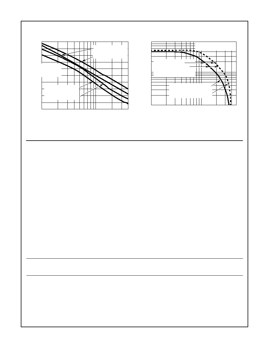
FIGURE 9. TURN-OFF DELAY vs COLLECTOR-EMITTER
CURRENT
FIGURE 10. OPERATING FREQUENCY vs COLLECTOR-
EMITTER CURRENT AND VOLTAGE
Typical Performance Curves
(Continued)
1
10
40
T
J
= +150
o
C
R
GE
= 25
L = 500
µ
H
I
CE
, COLLECTOR-EMITTER CURRENT (A)
V
CE
= 480V, V
GE
= 10V
1300
1200
1100
1000
900
800
700
600
500
400
300
V
CE
= 480V, V
GE
= 15V
V
CE
= 240V, V
GE
= 10V
V
CE
= 240V, V
GE
= 15V
t
D(OFF)I
, TURN-OFF DELA
Y (ns)
80
10
1
f
OP
, OPERA
TING FREQUENCY (kHz)
1
10
50
I
CE
, COLLECTOR-EMITTER CURRENT (A)
T
J
= +150
o
C, T
C
= +100
o
C,
R
GE
= 25
, L = 500
µ
H
V
CE
= 480V, V
GE
= 10V, 15V
f
MAX1
= 0.05/t
D(OFF)I
f
MAX2
= (P
D
- P
C
)/W
OFF
P
C
= DUTY FACTOR = 50%
R
JC
= 1.0
o
C/W
P
D
= ALLOWABLE DISSIPATION
P
C
= CONDUCTION DISSIPATION
NOTE:
V
CE
= 240V, V
GE
= 10V, 15V
Operating Frequency Information
Operating frequency information for a typical device (Figure
10) is presented as a guide for estimating device performance
for a specific application. Other typical frequency vs collector
current (I
CE
) plots are possible using the information shown
for a typical unit in Figures 7, 8 and 9. The operating
frequency plot (Figure 10) of a typical device shows f
MAX1
or
f
MAX2
whichever is smaller at each point. The information is
based on measurements of a typical device and is bounded
by the maximum rated junction temperature.
f
MAX1
is defined by f
MAX1
= 0.05/t
D(OFF)I
. t
D(OFF)I
deadtime
(the denominator) has been arbitrarily held to 10% of the on-
state time for a 50% duty factor. Other definitions are possible.
t
D(OFF)I
is defined as the time between the 90% point of the
trailing edge of the input pulse and the point where the
collector current falls to 90% of its maximum value. Device
turn-off delay can establish an additional frequency limiting
condition for an application other than T
JMAX
. t
D(OFF)I
is
important when controlling output ripple under a lightly loaded
condition.
f
MAX2
is defined by f
MAX2
= (P
D
- P
C
)/W
OFF
. The allowable
dissipation (P
D
) is defined by P
D
= (T
JMAX
- T
C
)/R
JC
. The sum
of device switching and conduction losses must not exceed P
D
.
A 50% duty factor was used (Figure 10) and the conduction
losses (P
C
) are approximated by P
C
= (V
CE
∑
I
CE
)/2. W
OFF
is
defined as the integral of the instantaneous power loss starting
at the trailing edge of the input pulse and ending at the point
where the collector current equals zero (I
CE
= 0A).
The switching power loss (Figure 10) is defined as f
MAX2
∑
W
OFF
.
Turn-on switching losses are not included because they can be
greatly influenced by external circuit conditions and components.