1
File Number
3123.2
CAUTION: These devices are sensitive to electrostatic discharge; follow proper IC Handling Procedures.
http://www.intersil.com or 407-727-9207 | Copyright © Intersil Corporation 1999
HI-201HS
High Speed, Quad SPST, CMOS Analog
Switch
The HI-201HS is a monolithic CMOS Analog Switch
featuring very fast switching speeds and low ON resistance.
The integrated circuit consists of four independently
selectable SPST switches and is pin compatible with the
industry standard HI-201 switch.
Fabricated using silicon-gate technology and the Intersil
Dielectric Isolation process, this TTL compatible device offers
improved performance over previously available CMOS analog
switches. Featuring maximum
switching times of 50ns, l
ow ON
resistance of 50
maximum, and a wide analog signal range, the
HI-201HS is designed for any application where improved
switching performance, particularly switching speed, is required.
(A more detailed discussion on the design and application of the
HI-201HS can be found in Application Note AN543.)
Features
∑ Fast Switching Times
- t
ON
. . . . . . . . . . . . . . . . . . . . . . . . . . . . . . . . . . . . 30ns
- t
OFF
. . . . . . . . . . . . . . . . . . . . . . . . . . . . . . . . . . . 40ns
∑ Low "ON" Resistance . . . . . . . . . . . . . . . . . . . . . . . . 30
∑ Pin Compatible with Standard HI-201
∑ Wide Analog Voltage Range (
±
15V Supplies) . . . . . . .
±
15V
∑ Low Charge Injection (
±
15V Supplies) . . . . . . . . . . 10pC
∑ TTL Compatible
∑ Symmetrical Switching Analog Current Range . . . . . 80mA
Applications
∑ High Speed Multiplexing
∑ High Frequency Analog Switching
∑ Sample and Hold Circuits
∑ Digital Filters
∑ Operational Amplifier Gain Switching Networks
∑ Integrator Reset Circuits
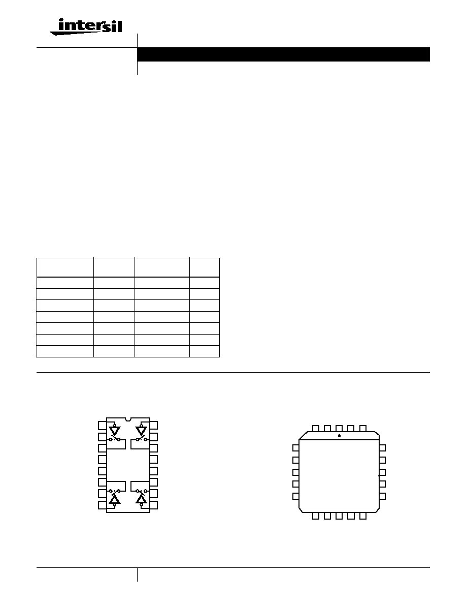
Pinouts
(Switches Shown For Logic "1" Input)
HI-201HS (CERDIP, PDIP, SOIC)
TOP VIEW
HI201HS (PLCC)
TOP VIEW
Ordering Information
PART NUMBER
TEMP.
RANGE (
o
C)
PACKAGE
PKG.
NO.
HI1-0201HS-2
-55 to 125
16 Ld CERDIP
F16.3
HI1-0201HS-4
-25 to 85
16 Ld CERDIP
F16.3
HI1-0201HS-5
0 to 75
16 Ld CERDIP
F16.3
HI3-0201HS-5
0 to 75
16 Ld PDIP
E16.3
HI4P0201HS-5
0 to 75
20 Ld PLCC
N20.35
HI9P0201HS-5
0 to 75
16 Ld SOIC
M16.3
HI9P0201HS-9
-40 to 85
16 Ld SOIC
M16.3
14
15
16
9
13
12
11
10
1
2
3
4
5
7
6
8
A
1
OUT1
IN1
V-
GND
IN4
A
4
OUT4
A
2
IN2
V+
NC
IN3
OUT3
A
3
OUT2
3
2
1
19
20
4
5
6
7
8
14
15
16
17
18
9
10
11
12
13
A
1
OUT 1
A
2
OUT 2
IN 1
V-
GND
IN 4
IN 2
V+
IN 3
OUT 4
OUT 3
A
4
A
3
Data Sheet
July 1999

2
Functional Diagram
TTL
LOGIC
INPUT
SWITCH
CELL
LEVEL
SHIFTER
AND
DRIVER
GATE
SOURCE
DRAIN
GATE
INPUT
OUTPUT
V-
V+
TRUTH TABLE
LOGIC
SWITCH
0
1
ON
OFF
Schematic Diagrams
TTL/CMOS REFERENCE CIRCUIT
SWITCH CELL
P41
V+
MP42
MP43
MP44
QP44
QN44
QN45
C49
C48
V
R1
QN43
R42
R41
QN41
QN42
D41
5V
D42
5.6V
QP42
QP41
V-
MN42
MN44
MN45
MP45
MP31
MN32
MP33
MN33
MN31
MP32
ANALOG
IN
ANALOG
OUT
Q
Q
V-
V+
HI-201HS
3
DIGITAL INPUT BUFFER AND LEVEL SHIFTER
Schematic Diagrams
(Continued)
M
N46
M
P51
I
Q
I
X3
I
X4
I
X1
Q
N6
Q
N7
V
R1
I
X2
I
X3
Q
P7
Q
P6
M
N52
M
N51
I
X1
I
X2
REPEAT FOR EACH
LEVEL SHIFTER
Q
N1
C
1
R
1
Q
P1
I
Q
Q
N4
Q
N8
Q
N9
M
P3
M
P4
Q
P9
Q
P8
M
P5
M
P7
C
FF
C
2
Q
N2
Q
N5
Q
P2
R
3
R
2
Q
P5
Q
P4
V
R1
M
P9
M
P6
M
P10
M
N3
M
N4
M
N5
M
N6
M
P8
M
N7
M
N8
M
N10
M
N9
M
P11
M
N11
V
EE
M
P12
M
N12
Q
M
P13
M
N13
V
CC
M
P14
M
N14
Q
M
P52
VA
HI-201HS

4
Absolute Maximum Ratings
Thermal Information
Supply Voltage (V+ to V-). . . . . . . . . . . . . . . . . . . . . . . . . . . . . . 36V
Digital Input Voltage . . . . . . . . . . . . . . . . . . . . . . (V+) +4V to (V-) -4V
Analog Input Voltage (One Switch) . . . . . . . (V+) +2.0V to (V-) -2.0V
Peak Current, S or D (Pulse 1ms, 10% Duty Cycle Max) . . . . 50mA
Continuous Current Any Terminal (Except S or D) . . . . . . . . . 25mA
Operating Conditions
Temperature Ranges
HI-201HS-2 . . . . . . . . . . . . . . . . . . . . . . . . . . . . . -55
o
C to 125
o
C
HI-201HS-4 . . . . . . . . . . . . . . . . . . . . . . . . . . . . . . -25
o
C to 85
o
C
HI-201HS-5 . . . . . . . . . . . . . . . . . . . . . . . . . . . . . . . . 0
o
C to 75
o
C
HI-201HS-9 . . . . . . . . . . . . . . . . . . . . . . . . . . . . . . -40
o
C to 85
o
C
Thermal Resistance (Typical, Note 1)
JA
(
o
C/W)
JC
(
o
C/W)
CERDIP Package . . . . . . . . . . . . . . . . .
80
30
PDIP Package . . . . . . . . . . . . . . . . . . .
90
N/A
PLCC Package . . . . . . . . . . . . . . . . . . .
80
N/A
SOIC Package . . . . . . . . . . . . . . . . . . .
100
N/A
Maximum Junction Temperature
Ceramic Package . . . . . . . . . . . . . . . . . . . . . . . . . . . . . . . . 175
o
C
Plastic Package . . . . . . . . . . . . . . . . . . . . . . . . . . . . . . . . . 150
o
C
Maximum Storage Temperature. . . . . . . . . . . . . . . . -65
o
C to 150
o
C
Maximum Lead Temperature (Soldering 10s) . . . . . . . . . . . . 300
o
C
(SOIC, PLCC - Lead Tips Only)
CAUTION: Stresses above those listed in "Absolute Maximum Ratings" may cause permanent damage to the device. This is a stress only rating and operation of the
device at these or any other conditions above those indicated in the operational sections of this specification is not implied.
NOTE:
1.
JA
is measured with the component mounted on an evaluation PC board in free air.
Electrical Specifications
Supplies = +15V, -15V; V
AH
(Logic Level High) = 2.4V, V
AL
(Logic Level Low) = +0.8V, GND = 0V,
Unless Otherwise Specified
PARAMETER
TEST
CONDITIONS
TEMP
(
o
C)
-2
-4, -5, -9
UNITS
MIN
TYP
MAX
MIN
TYP
MAX
DYNAMIC CHARACTERISTICS
Switch ON Time, t
ON
(Note 3)
25
-
30
50
-
30
50
ns
Switch OFF Time, t
OFF1
(Note 3)
25
-
40
50
-
40
50
ns
Switch OFF Time, t
OFF2
(Note 3)
25
-
150
-
-
150
-
ns
Output Settling Time
To 0.1%
25
-
180
-
-
180
-
ns
Charge Injection, Q
(Note 6)
25
-
10
-
-
10
-
pC
OFF Isolation
(Note 4)
25
-
72
-
-
72
-
dB
Crosstalk
(Note 5)
25
-
86
-
-
86
-
dB
Input Switch Capacitance, C
S(OFF)
25
-
10
-
-
10
-
pF
Output Switch Capacitance
C
D(OFF)
25
-
10
-
-
10
-
pF
C
D(ON)
25
-
30
-
-
30
-
pF
Digital Input Capacitance, C
A
25
-
18
-
-
18
-
pF
Drain-To-Source Capacitance, C
DS(OFF)
25
-
0.5
-
-
0.5
-
pF
DIGITAL INPUT CHARACTERISTICS
Input Low Threshold, V
AL
Full
-
-
0.8
-
-
0.8
V
Input High Threshold, V
AH
25
2.0
-
-
2.0
-
-
V
Full
2.4
-
-
2.4
-
-
V
Input Leakage Current (Low), I
AL
25
-
200
-
-
200
-
µ
A
Full
-
-
500
-
-
500
µ
A
Input Leakage Current (High), I
AH
V
AH
= 4.0V
25
-
20
-
-
20
-
µ
A
Full
-
-
40
-
-
40
µ
A
ANALOG SWITCH CHARACTERISTICS
Analog Signal Range, V
S
Full
-15
-
+15
-15
-
+15
V
ON Resistance, r
ON
(Note 2)
25
-
30
50
-
30
50
Full
-
-
75
-
-
75
HI-201HS

5
r
ON
Match
25
-
3
-
-
3
-
%
OFF Input Leakage Current, I
S(OFF)
25
-
0.3
10
-
0.3
10
nA
Full
-
-
100
-
-
50
nA
OFF Output Leakage Current, I
D(OFF)
25
-
0.3
10
-
0.3
10
nA
Full
-
-
100
-
-
50
nA
ON Leakage Current, I
D(ON)
25
-
0.1
10
-
0.1
10
nA
Full
-
-
100
-
-
50
nA
POWER SUPPLY CHARACTERISTICS (Note 7)
Power Dissipation, P
D
25
-
120
-
-
120
-
mW
Full
-
-
240
-
-
240
mW
Current, I+ (Pin 13)
25
-
4.5
-
-
4.5
-
mA
Full
-
-
10.0
-
-
10.0
mA
Current, I- (Pin 4)
25
-
3.5
-
-
3.5
-
mA
Full
-
-
6
-
-
6
mA
NOTES:
2. V
OUT
=
±
10V, I
OUT
= 1mA.
3. R
L
= 1k
, C
L
= 35pF, V
IN
= +10V, V
A
= +3V. (See Figure 1).
4. V
A
= 3V, R
L
= 1k
, C
L
= 10pF, V
IN
= 3V
RMS
, f = 100kHz.
5. V
A
= 3V, R
L
= 1k
, V
IN
= 3V
RMS
, f = 100kHz.
6. C
L
= 1nF, V
IN
= 0V, Q = C
L
x
V
O
.
7. V
A
= 3V or V
A
= 0 for all switches.
Electrical Specifications
Supplies = +15V, -15V; V
AH
(Logic Level High) = 2.4V, V
AL
(Logic Level Low) = +0.8V, GND = 0V,
Unless Otherwise Specified (Continued)
PARAMETER
TEST
CONDITIONS
TEMP
(
o
C)
-2
-4, -5, -9
UNITS
MIN
TYP
MAX
MIN
TYP
MAX
Test Circuits and Waveforms
FIGURE 1A. MEASUREMENT POINTS
FIGURE 1B. WAVEFORMS
DIGITAL
INPUT
SWITCH
OUTPUT
V
AH
= 3.0V
50%
V
AL
= 0V
90%
10%
t
ON
50%
0V
90%
t
OFF2
t
OFF1
TOP: Logic Input (2V/Div.)
BOTTOM: Output (5V/Div.)
HORIZONTAL: 100ns/Div.
HI-201HS