4-1069
August 1997
HI1175
8-Bit, 20 MSPS, Flash A/D Converter
Features
∑ Resolution . . . . . . . . . . . . . . . . . . 8-Bit
±
0.3 LSB (DNL)
∑ Maximum Sampling Frequency . . . . . . . . . . . 20 MSPS
∑ Low Power Consumption . . . . 60mW (at 20 MSPS Typ)
(Reference Current Excluded)
∑ Built-In Sample and Hold Circuit
∑ Built-In Reference Voltage Self Bias Circuit
∑ Three-State TTL Compatible Output
∑ Single +5V Power Supply
∑ Low Input Capacitance . . . . . . . . . . . . . . . . . 11pF (Typ)
∑ Reference Impedance . . . . . . . . . . . . . . . . . . 300
(Typ)
∑ Evaluation Board Available (HI1175-EV)
∑ Low Cost
∑ Direct Replacement for the Sony CXD1175
Applications
∑ Video Digitizing
∑ PC Video Capture
∑ Image Scanners
∑ TV Set Top Boxes
∑ Multimedia
∑ Personal Communication
Systems (PCS)
Description
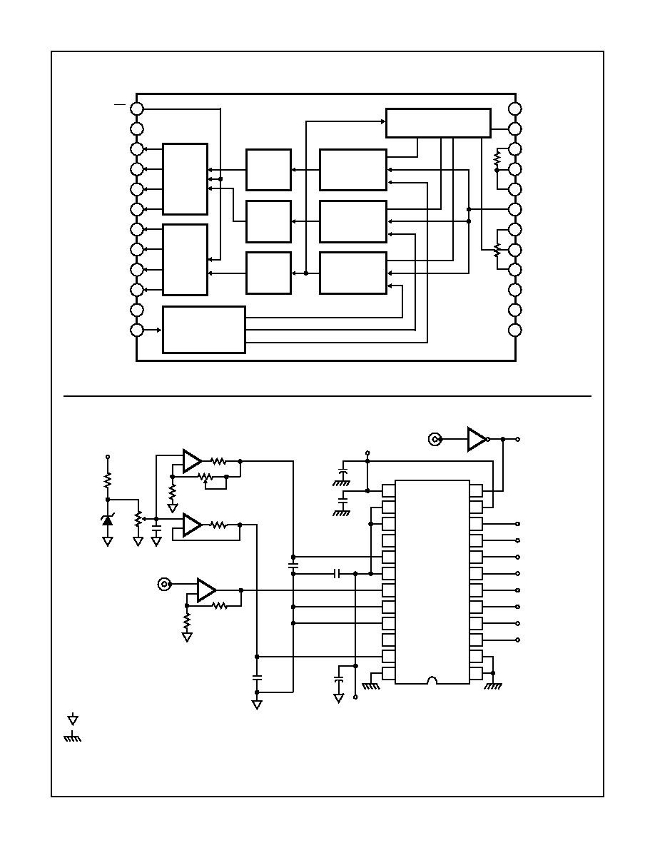
The HI1175 is an 8-bit, analog-to-digital converter built in a
1.4
µ
m CMOS process. The low power, low differential gain
and phase, high sampling rate, and single 5V supply make
the HI1175 ideal for video and imaging applications.
The adoption of a 2-step flash architecture achieves low
power consumption (60mW) at a maximum conversion
speed of 20 MSPS (Min), 35 MSPS typical with only a 2.5
clock cycle data latency. The HI1175 also features digital
output enable/disable and a built in voltage reference. The
HI1175 can be configured to use the internal reference or an
external reference if higher precision is required.
Pinout
HI1175 (PDIP, SOIC)
TOP VIEW
Ordering Information
PART NUMBER
TEMP.
RANGE (
o
C)
PACKAGE
PKG.
NO.
HI1175JCP
-40 to 85
24 Ld PDIP
E24.4-S
HI1175JCB
-40 to 85
24 Ld SOIC
M24.2-S
HI1175-EV
25
Evaluation Board
DV
SS
D0 (LSB)
D1
D2
D3
D4
D6
D5
DV
DD
CLK
V
RB
AV
SS
V
IN
AV
DD
V
RBS
V
RT
V
RTS
AV
DD
AV
DD
DV
DD
OE
DV
SS
1
2
3
4
5
6
7
8
9
10
11
12
16
17
18
19
20
21
22
23
24
15
14
13
D7 (MSB)
AV
SS
File Number
3577.6
CAUTION: These devices are sensitive to electrostatic discharge; follow proper IC Handling Procedures.
http://www.intersil.com or 407-727-9207
|
Copyright
©
Intersil Corporation 1999
4-1072
Absolute Maximum Ratings
Thermal Information
Supply Voltage, V
DD
. . . . . . . . . . . . . . . . . . . . . . . . . . . . . . . . . . . 7V
Reference Voltage, V
RT
, V
RB
. . . . . . . . . . . . . . . . . . . . . V
DD
to V
SS
Analog Input Voltage, V
IN
. . . . . . . . . . . . . . . . . . . . . . . . V
DD
to V
SS
Digital Input Voltage, CLK. . . . . . . . . . . . . . . . . . . . . . . . V
DD
to V
SS
Digital Output Voltage, V
OH
, V
OL
. . . . . . . . . . . . . . . . . . V
DD
to V
SS
Operating Conditions
(Note 1)
Temperature Range, T
A
. . . . . . . . . . . . . . . . . . . . . . . -40
o
C to 85
o
C
Supply Voltage
AV
DD
, AV
SS
, DV
DD
, DV
SS
. . . . . . . . . . . . . . . +4.75V to +5.25V
|DGND-AGND| . . . . . . . . . . . . . . . . . . . . . . . . . . . .0mV to 100mV
Reference Input Voltage
V
RB
. . . . . . . . . . . . . . . . . . . . . . . . . . . . . . . . . . . . . 0V and Above
V
RT
. . . . . . . . . . . . . . . . . . . . . . . . . . . . . . . . . . . . 2.8V and Below
Analog Input Range, V
IN
. . . . . . . V
RB
to V
RT
(1.8V
P-P
to 2.8V
P-P
)
Clock Pulse Width
t
PW1
. . . . . . . . . . . . . . . . . . . . . . . . . . . . . . . . . . . . . . . 25ns (Min)
t
PW0
. . . . . . . . . . . . . . . . . . . . . . . . . . . . . . . . . . . . . . . 25ns (Min)
Thermal Resistance (Typical, Note 1)
JA
(
o
C/W)
PDIP Package . . . . . . . . . . . . . . . . . . . . . . . . . . . . .
78
SOIC Package . . . . . . . . . . . . . . . . . . . . . . . . . . . . .
98
Maximum Junction Temperature . . . . . . . . . . . . . . . . . . . . . 150
o
C
Maximum Storage Temperature Range, T
STG
. . . . .-65
o
C to 150
o
C
Maximum Lead Temperature (Soldering 10s) . . . . . . . . . . . . 300
o
C
(SOIC - Lead Tips Only)
CAUTION: Stresses above those listed in "Absolute Maximum Ratings" may cause permanent damage to the device. This is a stress only rating and operation of
the device at these or any other conditions above those indicated in the operational sections of this specification is not implied.
NOTE:
1.
JA
is measured with the component mounted on an evaluation PC board in free air.
Electrical Specifications
f
C
= 20 MSPS, V
DD
= +5V, V
RB
= 0.5V, V
RT
= 2.5V, T
A
= 25
o
C (Note 1)
PARAMETER
TEST CONDITIONS
MIN
TYP
MAX
UNIT
SYSTEM PERFORMANCE
Offset Voltage
E
OT
-60
-35
-10
mV
E
OB
0
+15
+45
mV
Integral Non-Linearity, INL
f
C
= 20 MSPS, V
IN
= 0.6V to 2.6V
-
±
0.5
±
1.3
LSB
Differential Non-Linearity, DNL
f
C
= 20 MSPS, V
IN
= 0.6V to 2.6V
-
±
0.3
±
0.5
LSB
DYNAMIC CHARACTERISTICS
Effective Number of Bits, ENOB
f
IN
= 1MHz
-
7.6
-
Bits
Spurious Free Dynamic Range
f
IN
= 1MHz
-
51
-
dB
Signal to Noise Ratio, SINAD
f
C
= 20MHz, f
IN
= 1MHz
-
46
-
dB
f
C
= 20MHz, f
IN
= 3.58MHz
-
46
-
dB
Maximum Conversion Speed, f
C
V
IN
= 0.6V to 2.6V, f
IN
= 1kHz Ramp
20
35
-
MSPS
Minimum Conversion Speed
-
-
0.5
MSPS
Differential Gain Error, DG
NTSC 40 IRE Mod Ramp, f
C
= 14.3 MSPS
-
1.0
-
%
Differential Phase Error, DP
-
0.5
-
Degree
Aperture Jitter, t
AJ
-
30
-
ps
Sampling Delay, t
DS
-
4
-
ns
Data Latency, t
LAT
-
-
2.5
Cycles
ANALOG INPUTS
Analog Input Bandwidth (-1dB), BW
-
18
-
MHz
Analog Input Capacitance, C
IN
V
IN
= 1.5V + 0.07V
RMS
-
11
-
pF
RMS Signal
RMS Noise
Distor tion
+
------------------------------------------------------------------
=
HI1175