
1
Æ
FN3141.4
HI-1818A
Low Resistance, Single 8-Channel, CMOS
Analog Multiplexer
The Hl-1818A is a monolithic, high performance CMOS
analog multiplexer offering built-in channel selection
decoding plus an inhibit (enable) input for disabling all
channels. Dielectric Isolation (Dl) processing is used for
enhanced reliability and performance. Substrate leakage
and parasitic capacitance are much lower, resulting in
extremely low static errors and high throughput rates. Low
output leakage (typically 0.1nA) and low channel ON
resistance (250
) assure optimum performance in low level
or current mode applications.
The HI-1818A is a single-ended, 8-Channel multiplexer, and is
ideally suited for medical instrumentation, telemetry systems,
and microprocessor based data acquisition systems.
Features
∑ Signal Range . . . . . . . . . . . . . . . . . . . . . . . . . . . . . . .+15V
∑ "ON" Resistance . . . . . . . . . . . . . . . . . . . . . . . . . . . 250
∑ Input Leakage (Max) . . . . . . . . . . . . . . . . . . . . . . . . .50nA
∑ Access Time . . . . . . . . . . . . . . . . . . . . . . . . . . . . . 350ns
∑ Power Consumption . . . . . . . . . . . . . . . . . . . . . . . . . 5mW
∑ DTL/TTL Compatible Address
∑ Operation . . . . . . . . . . . . . . . . . . . . . . . . . -55
o
C to 125
o
C
Applications
∑ Data Acquisition Systems
∑ Precision Instrumentation
∑ Demultiplexing
∑ Selector Switch
Ordering Information
PART NUMBER
TEMP.
RANGE (
o
C)
PACKAGE
PKG.
DWG. #
HI1-1818A-2
-55 to 125
16 Ld CERDIP
F16.3
Pinout
HI-1818A (CERDIP)
TOP VIEW
14
15
16
9
13
12
11
10
1
2
3
4
5
7
6
8
ADDRESS A
1
+5V SUPPLY
ENABLE
ADDRESS A
2
IN 8
IN 7
IN 5
IN 6
ADDRESS A
0
+V
SUPPLY
IN 1
OUT
IN 2
IN 3
IN 4
-V
SUPPLY
Data Sheet
November 19, 2004
CAUTION: These devices are sensitive to electrostatic discharge; follow proper IC Handling Procedures.
1-888-INTERSIL or 321-724-7143
|
Intersil (and design) is a trademark of Intersil Americas Inc.
Copyright © Intersil Americas Inc. 2002, 2004. All Rights Reserved

2
FN3141.4
November 19, 2004
Truth Table
Functional Block Diagram
HI-1818A
HI-1818A TRUTH TABLE
ADDRESS
"ON" CHANNEL
A
2
A
1
A
0
EN
L
L
L
L
1
L
L
H
L
2
L
H
L
L
3
L
H
H
L
4
H
L
L
L
5
H
L
H
L
6
H
H
L
L
7
H
H
H
L
8
X
X
X
H
None
HI-1818A TRUTH TABLE
ADDRESS
"ON" CHANNEL
A
2
A
1
A
0
EN
N
A
0
A
1
A
2
ENABLE
DIGITAL ADDRESS
ENABLE
BUFFER
DECODERS
P
MULTIPLEX
SWITCHES
N
P
IN 1
OUT
IN 8
ADDRESS
INPUT
BUFFERS
Schematic Diagrams
All N-Channel Bodies to V-
All P-Channel Bodies to V+
Unless Otherwise Specified
ADDRESS INPUT BUFFER
N9
P9
N10
P10
N8
P8
N7
P7
N6
P6
N5
N4
N3
V-
N1
P1
P2
N2
P5
P4
V
CC
V+
V-
ADDRESS
INPUT
D1
D2
200
P3
A
A
HI-1818A

3
FN3141.4
November 19, 2004
All N-Channel Bodies to V-
All P-Channel Bodies to V+
ADDRESS DECODER
All N-Channel Bodies to V-
All P-Channel Bodies to V+
Unless Otherwise Specified
MULTIPLEXER SWITCH
Schematic Diagrams
V+
V-
A0 OR
A0
N14
N13
A1 OR
A1
N12
N11
A2 OR
A2
EN
P14
P13
P12
P11
N15
P15
N16
P16
TO P-CHANNEL
SWITCH
TO N-CHANNEL
SWITCH
IN SWITCH CELL
V+
N18
N17
N19
P17
P18
FROM DECODE
FROM DECODE
V+
OUT
IN
HI-1818A

4
FN3141.4
November 19, 2004
Absolute Maximum Ratings
Thermal Information
V+ to V- . . . . . . . . . . . . . . . . . . . . . . . . . . . . . . . . . . . . . . . . . . . 40V
Logic Supply Voltage . . . . . . . . . . . . . . . . . . . . . . . . . . . . . . . . . 30V
Analog Signal (V
IN
, V
OUT
). . . . . . . . . . . . . . . . . (V-) -2V to (V+) +2V
Digital Input Voltage (V
EN
, V
A
) . . . . . . . . . . . . . . . . . . . . (V-) to (V+)
Operating Conditions
Temperature Range . . . . . . . . . . . . . . . . . . . . . . . . . -55
o
C to 125
o
C
Thermal Resistance (Typical, Note 1)
JA
(
o
C/W)
JC
(
o
C/W)
CERDIP Package. . . . . . . . . . . . . . . . .
80
20
Maximum Junction Temperature
Ceramic Package . . . . . . . . . . . . . . . . . . . . . . . . . . . . . . . . 175
o
C
Maximum Storage Temperature Range . . . . . . . . . . -65
o
C to 150
o
C
Maximum Lead Temperature (Soldering 10s) . . . . . . . . . . . . 300
o
C
CAUTION: Stresses above those listed in "Absolute Maximum Ratings" may cause permanent damage to the device. This is a stress only rating and operation of the
device at these or any other conditions above those indicated in the operational sections of this specification is not implied.
NOTE:
1.
JA
is measured with the component mounted on a low effective thermal conductivity test board in free air. See Tech Brief 379 for details.
Electrical Specifications
Supplies = +15V, -15V, +5V; V
AL
= 0.4V, V
AH
= 4.0V, Unless Otherwise Specified
PARAMETER
TEST CONDITIONS
TEMP (
o
C)
MIN
TYP
MAX
UNITS
DYNAMIC CHARACTERISTICS
Access Time, t
A
Note 4
25
-
350
500
ns
Full
-
-
1000
ns
Break-Before-Make Delay, t
OPEN
25
-
25
-
ns
Enable Delay (ON), t
ON(EN)
25
-
300
500
ns
Full
-
-
1000
ns
Enable Delay (OFF), t
OFF(EN)
25
-
300
500
ns
Full
-
-
1000
ns
Settling Time
To 0.1%
25
-
1.08
-
µ
s
To 0.025%
25
-
2.8
-
µ
s
Channel Input Capacitance, C
S(OFF)
25
-
4
-
pF
Channel Output Capacitance, C
D(OFF)
25
-
20
-
pF
Input to Output Capacitance, C
DS(OFF)
25
-
0.6
-
pF
Digital Input Capacitance, C
A
25
-
5
-
pF
DIGITAL INPUT CHARACTERISTICS
Input Low Threshold, V
AL
Full
-
-
0.4
V
Input High Threshold, V
AH
Note 3
Full
4.0
-
-
V
Input Leakage Current, I
A
Full
-
-
1
µ
A
ANALOG CHANNEL CHARACTERISTICS
Analog Signal Range, V
lN
Full
-15
-
+15
V
ON Resistance, r
ON
Note 2
25
-
250
400
Full
-
-
500
OFF Input Leakage Current, I
S(OFF)
Full
-
-
50
nA
ON Channel Leakage Current, l
D(ON)
Full
-
-
250
nA
OFF Output Leakage Current, I
D(OFF)
Full
-
-
250
nA
HI-1818A
5
FN3141.4
November 19, 2004
POWER SUPPLY CHARACTERISTICS
Power Dissipation, P
D
Full
-
-
27.5
mW
Current, I+
Full
-
-
0.5
mA
Current, I-
Full
-
-
1
mA
Current, I
L
Full
-
-
1
mA
NOTES:
2. V
OUT
=
±
10V, I
OUT
=
1mA.
3. To drive from DTL/TTL circuits, 1k
pull-up resistors to 5.0V supply are recommended.
4. Time measured to 90% of final output level; V
OUT
= -5.0V to 5.0V, Digital Inputs = 0V to 4.0V.
Electrical Specifications
Supplies = +15V, -15V, +5V; V
AL
= 0.4V, V
AH
= 4.0V, Unless Otherwise Specified (Continued)
PARAMETER
TEST CONDITIONS
TEMP (
o
C)
MIN
TYP
MAX
UNITS
±
Test Circuits and Waveforms
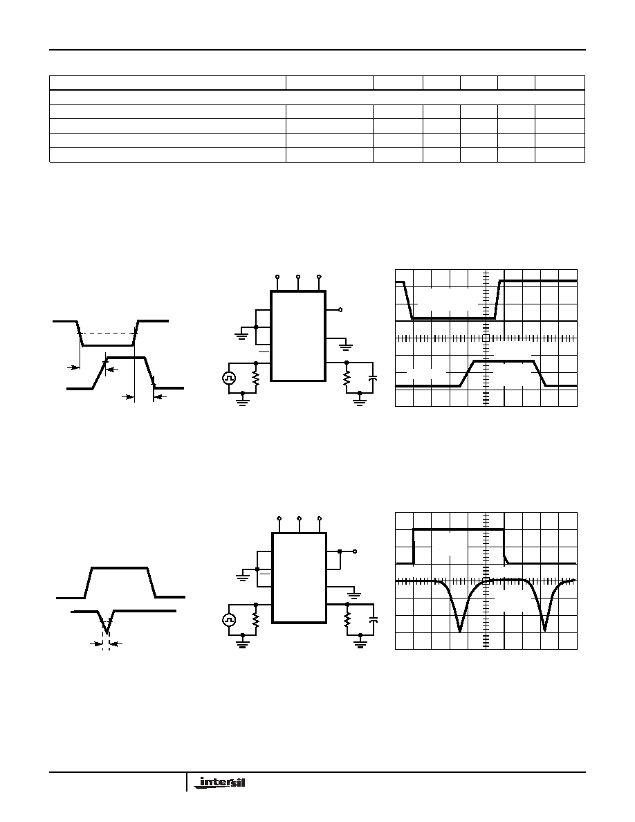
FIGURE 1A. MEASUREMENT POINTS
FIGURE 1B. TEST CIRCUIT
FIGURE 1C. WAVEFORMS
FIGURE 1. ENABLE DELAYS
FIGURE 2A. MEASUREMENT POINTS
FIGURE 2B. TEST CIRCUIT
FIGURE 2C. WAVEFORMS
FIGURE 2. BREAK-BEFORE-MAKE DELAY
V
AH
= 4.0V
V
AL
= 0V
OUTPUT
10%
t
OFF
(EN)
90%
t
ON
(EN)
50%
ENABLE DRIVE
(V
A
)
+15V
V
A
+5V
-15V +5V
V+
V-
V
L
IN 1
IN 2-8
OUT
HI-1818A
200
12.5
50
A
0
EN
A
1
A
2
pF
ENABLE DRIVE
2V/DIV.
OUTPUT
2V/DIV.
100ns/DIV.
ENABLED
(S
1
ON)
DISABLED
50%
50%
0V
4.0V
ADDRESS
DRIVE (V
A
)
t
OPEN
OUTPUT
+15V
V
A
+5V
-15V +5V
V+
V-
V
L
IN 1
IN 2
IN 3-8
OUT
HI-1818A
50
A
0
EN
A
1
A
2
200
12.5
pF
V
A
INPUT
2V/DIV.
OUTPUT
1V/DIV.
100ns/DIV.
S
2
ON
S
1
ON
HI-1818A