HI-565A
1
®
FN3109.4
HI-565A
High Speed, Monolithic D/A Converter
with Reference
The HI-565A is a fast, 12-bit, current output, digital-to-analog
converter. The monolithic chip includes a precision voltage
reference, thin-film R2R ladder, reference control amplifier
and twelve high speed bipolar current switches.
The Intersil dielectric isolation process provides latch free
operation while minimizing stray capacitance and leakage
currents, to produce an excellent combination of speed and
accuracy. Also, ground currents are minimized to produce a
low and constant current through the ground terminal, which
reduces error due to code dependent ground currents.
HI-565A dice are laser trimmed for a maximum integral
nonlinearity error of
±
0.5 LSB at 25
o
C. In addition, the low
noise buried zener reference is trimmed both for absolute
value and temperature coefficient. Power dissipation is
typically 250mW, with
±
15V supplies.
The HI-565A is offered in both commercial and military
grades. See Ordering Information.
Features
· 12-Bit DAC and Reference on a Single Chip
· Pin Compatible With AD565A
· Very High Speed: Settles to
±
0.5 LSB in 250ns (Max)
Full Scale Switching Time 30ns (Typ)
· Guaranteed For Operation With
±
12V Supplies
· Monotonicity Guaranteed Over Temperature
· Nonlinearity Guaranteed Over Temp (Max) . . . .
±
0.5 LSB
· Low Gain Drift (Max, DAC Plus Ref) . . . . . . . . .25ppm/
o
C
· Low Power Dissipation . . . . . . . . . . . . . . . . . . . . .250mW
Applications
· CRT Displays
· High Speed A/D Converters
· Signal Reconstruction
· Waveform Synthesis
Ordering Information
PART NUMBER
LINEARITY (INL)
LINEARITY (DNL)
TEMP. RANGE (
o
C)
PACKAGE
PKG. NO.
HI1-565AJD-5
0.50 LSB
0.75 LSB
0 to 75
24 Ld SBDIP
D24.6
HI1-565ATD-2
0.25 LSB
0.50 LSB
-55 to 125
24 Ld SBDIP
D24.6
HI1-565ASD/883
0.50 LSB
0.50 LSB
-55 to 125
24 Ld SBDIP
D24.6
HI1-565ATD/883
0.25 LSB
0.50 LSB
-55 to 125
24 Ld SBDIP
D24.6
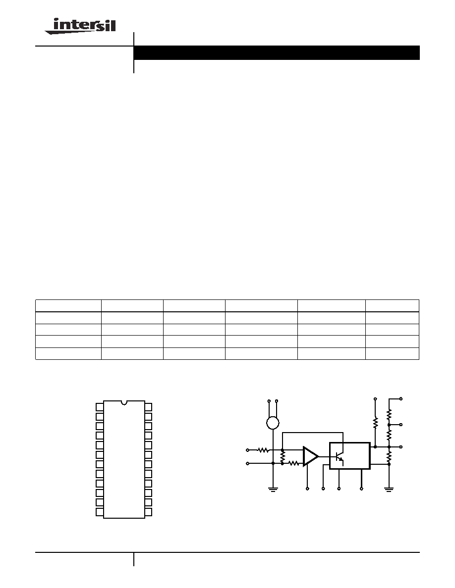
Pinout
HI-565A (SBDIP)
TOP VIEW
Functional Diagram
1
2
3
4
5
6
7
8
9
10
11
12
NC
NC
V
CC
REF OUT (+10V)
REF GND
REF IN
-V
EE
BIPOLAR R IN
IDAC OUT
10V SPAN R
20V SPAN R
POWER GND
16
17
18
19
20
21
22
23
24
15
14
13
BIT 1 (MSB) IN
BIT 3 IN
BIT 4 IN
BIT 5 IN
BIT 6 IN
BIT 8 IN
BIT 10 IN
BIT 11 IN
BIT 12 (LSB) IN
BIT 2 IN
BIT 7 IN
BIT 9 IN
REF
V
CC
4
3
+
-
6
REF
IN
19.95K
5
REF
GND
3.5K
3K
I
REF
0.5mA
7
12
-V
EE
PWR
GND
MSB
LSB
HI-565A
24 . . .
. . .13
BIP. OFF
8
9.95K
DAC
I
O
(4X I
REF
X CODE)
11 20V
SPAN
10V
SPAN
OUT
10
9
2.5K
5K
5K
OUT
+
-
Data Sheet
May 2002
CAUTION: These devices are sensitive to electrostatic discharge; follow proper IC Handling Procedures.
1-888-INTERSIL or 321-724-7143
|
Intersil (and design) is a registered trademark of Intersil Americas Inc.
Copyright © Intersil Americas Inc. 2002. All Rights Reserved
2
Absolute Maximum Ratings
Thermal Information
V
CC
to Power GND . . . . . . . . . . . . . . . . . . . . . . . . . . . . . 0V to +18V
V
EE
to Power GND . . . . . . . . . . . . . . . . . . . . . . . . . . . . . 0V to -18V
Voltage on DAC Output (Pin 9) . . . . . . . . . . . . . . . . . . . -3V to +12V
Digital Inputs (Pins 13-24) to Power GND . . . . . . . . . . . -1V to +7.0V
REF In to REF GND. . . . . . . . . . . . . . . . . . . . . . . . . . . . . . . . .
±
12V
Bipolar Offset to REF GND . . . . . . . . . . . . . . . . . . . . . . . . . . .
±
12V
10V Span R to REF GND . . . . . . . . . . . . . . . . . . . . . . . . . . . .
±
12V
20V Span R to REF GND . . . . . . . . . . . . . . . . . . . . . . . . . . . .
±
24V
REF Out . . . . . . . . . . . . . . . . . . . . . . Indefinite Short to Power GND,
Momentary Short to V
CC
Operating Conditions
Temperature Ranges
HI1-565AX-2, /883 . . . . . . . . . . . . . . . . . . . . . . . . -55
o
C to 125
o
C
HI1-565AX-5. . . . . . . . . . . . . . . . . . . . . . . . . . . . . . . . 0
o
C to 75
o
C
Thermal Resistance (Typical, Note 1)
JA
(
o
C/W)
JC
(
o
C/W)
SBDIP Package . . . . . . . . . . . . . . . . . .
60
20
Maximum Package Power Dissipation
SBDIP Package . . . . . . . . . . . . . . . . . . . . . . . . . . . . . . . . .500mW
Maximum Junction Temperature . . . . . . . . . . . . . . . . . . . . . . .175
o
C
Maximum Storage Temperature Range . . . . . . . . . -65
o
C to 150
o
C
Maximum Lead Temperature (Soldering 10s) . . . . . . . . . . . . .300
o
C
Die Characteristics
Transistor Count . . . . . . . . . . . . . . . . . . . . . . . . . . . . . . . . . . . . . 200
Process . . . . . . . . . . . . . . . . . . . . . . . . . . . . . . . . . . . . . . . Bipolar-DI
CAUTION: Stresses above those listed in "Absolute Maximum Ratings" may cause permanent damage to the device. This is a stress only rating and operation of the
device at these or any other conditions above those indicated in the operational sections of this specification is not implied.
NOTE:
1.
JA
is measured with the component mounted on an evaluation PC board in free air.
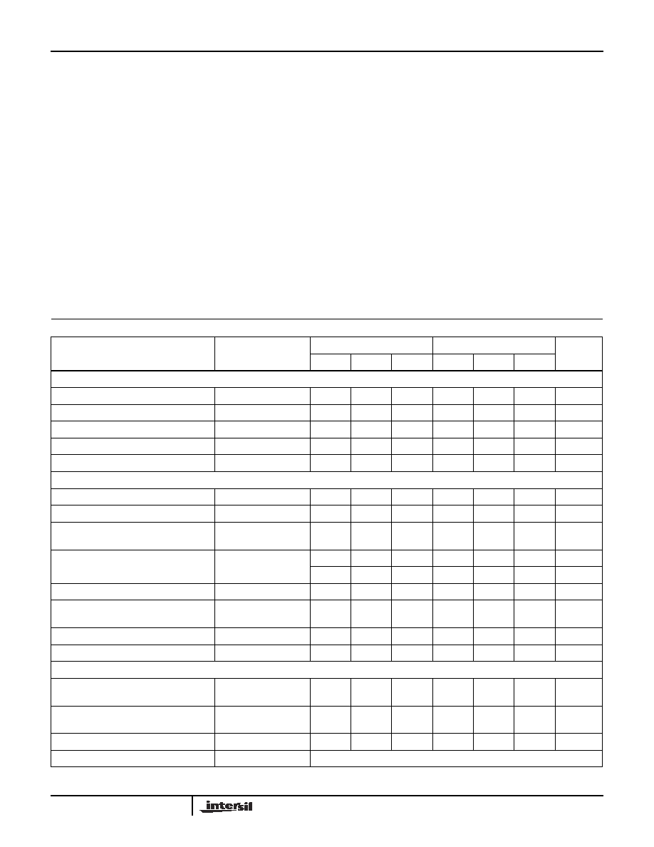
Electrical Specifications
T
A
= 25
o
C, V
CC
= +15V, V
EE
= -15V, Unless Otherwise Specified
PARAMETER
TEST CONDITIONS
HI-565AJ, HI-565AS
HI-565AT
UNITS
MIN
TYP
MAX
MIN
TYP
MAX
DATA INPUTS (Pins 13 to 24)
Input Voltage Bit ON Logic "1"
(T
MlN
to T
MAX
)
+2.0
-
+5.5
+2.0
-
+5.5
V
Input Voltage Bit OFF Logic "0"
(T
MlN
to T
MAX
)
-
-
+0.8
-
-
+0.8
V
Logic Current Bit ON Logic "1"
(T
MlN
to T
MAX
)
-
0.01
+1.0
-
0.01
+1.0
µ
A
Logic Current Bit OFF Logic "0"
(T
MlN
to T
MAX
)
-
-2.0
-20
-
-2.0
-20
µ
A
Resolution
(Note 2)
12
-
-
12
-
-
Bits
OUTPUT
Unipolar Current
(All Bits ON)
-1.6
-2.0
-2.4
-1.6
-2.0
-2.4
mA
Bipolar Current
(All Bits ON or OFF)
±
0.8
±
1.0
±
1.2
±
0.8
±
1.0
±
1.2
mA
Resistance
(Exclusive of Span
Resistors) (Note 2)
1.8K
2.5K
3.2K
1.8K
2.5K
3.2K
Unipolar Offset (25
o
C)
-0.05
0.01
0.05
-0.05
0.01
0.05
% of FS
-0.07
0.01
0.07
-0.07
0.01
0.07
% of FS
Bipolar Offset (25
o
C)
-0.15
0.05
0.15
-0.1
0.05
0.1
% of FS
Bipolar Offset (T
MlN
to T
MAX
)
/883 Versions Only
(Figure 2, R
3
= 50
)
-0.25
0.05
0.25
-0.2
0.05
0.2
% of FS
Capacitance
-
20
-
-
20
-
pF
Compliance Voltage
(T
MIN
to T
MAX
)(Note 2)
-1.5
-
+10
-1.5
-
+10
V
ACCURACY (Error Relative to Full Scale)
Integral Non-Linearity
(25
o
C)
End Point Method
-
±
0.25
(0.006)
±
0.50
(0.012)
-
±
0.12
(0.003)
±
0.25
(0.006)
LSB
% of FS
Integral Non-Linearity
/883 Versions Only
(T
MIN
to T
MAX
)
End Point Method
-
±
0.50
(0.012)
±
0.75
(0.018)
-
±
0.25
(0.006)
±
0.50
(0.012)
LSB
% of FS
Differential Non-Linearity
25
o
C
-
±
0.50
±
0.75
-
±
0.25
±
0.50
LSB
Differential Non-Linearity
T
MIN
to T
MAX
MONOTONICITY GUARANTEED
HI-565A
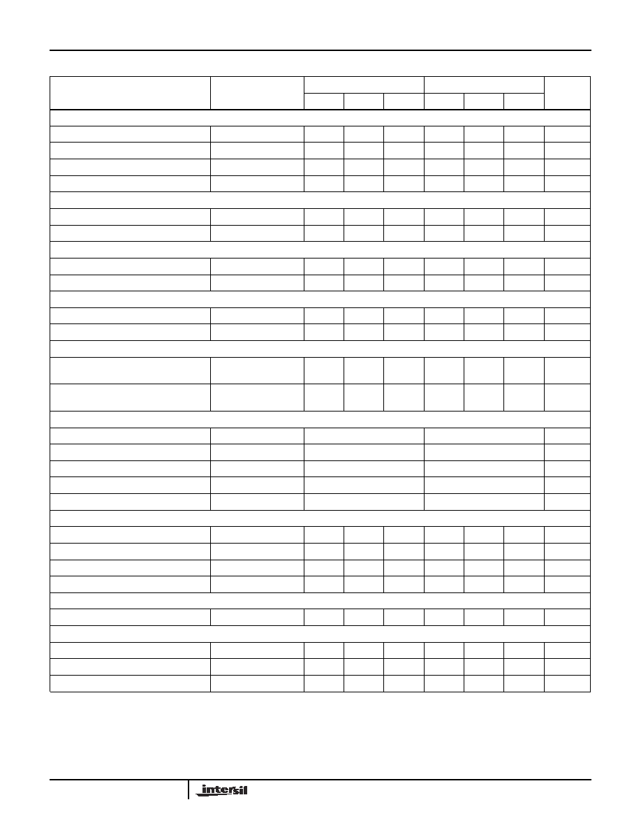
3
TEMPERATURE COEFFIClENTS
Unipolar Offset Drift
-
1
2
-
1
2
ppm/
o
C
Bipolar Zero Drift
Internal Reference
-
5
10
-
5
10
ppm/
o
C
Gain Drift, Uni- and Bipolar (Full Scale)
Internal Reference
-
15
40
-
10
25
ppm/
o
C
Differential Nonlinearity Error Drift
Int. Ref.
-
2
-
-
2
-
ppm/
o
C
SETTLING TIME T0
±
0.5 LSB
With High, Z External Load
(Notes 2, 3)
-
350
500
-
350
500
ns
With 75
External Load
(Notes 2, 3)
-
150
250
-
150
250
ns
FULL SCALE TRANSITION From 50% of Logic Input to 90% of Analog Output
Rise Time
(Note 2)
-
15
30
-
15
30
ns
Fall Time
(Note 2)
-
30
50
-
30
50
ns
POWER REQUIREMENTS
I
CC
-
9.0
11.8
-
9.0
11.8
mA
I
EE
-
-9.5
-14.5
-
-9.5
-14.5
mA
POWER SUPPLY GAIN SENSITIVITY (Note 4)
V
CC
(+11.4 to +16.5V
DC
)
All Bits = 2V, Unipolar
-
3
10
-
3
10
ppm of
FS/%
V
EE
(-11.4 to -16.5V
DC
)
All Bits = 2V, Unipolar
-
15
25
-
15
25
ppm of
FS/%
PROGRAMMABLE OUTPUT RANGES (See Table 2)
Unipolar 5
(Note 2)
0 to +5
0 to +5
V
Bipolar 5
(Note 2)
-2.5 to +2.5
-2.5 to +2.5
V
Unipolar 10
(Note 2)
0 to +10
0 to +10
V
Bipolar 10
(Note 2)
-5 to +5
-5 to +5
V
Bipolar 20
(Note 2)
-10 to +10
-10 to +10
V
EXTERNAL ADJUSTMENTS
Gain Error
R2 = 50
(Figure 2)
-
±
0.1
±
0.25
-
±
0.1
±
0.25
% of FS
Bipolar Zero Error
R3 = 50
(Figure 3)
-
±
0.05
±
0.15
-
±
0.05
±
0.1
% of FS
Gain Adjustment Range
(Figure 1) (Note 2)
±
0.25
-
-
±
0.25
-
-
% of FS
Bipolar Zero Adjustment Range
(Note 2)
±
0.15
-
-
±
0.15
-
-
% of FS
REFERENCE INPUT
Input Impedance
(Note 2)
15K
20K
25K
15K
20K
25K
REFERENCE OUTPUT
Voltage, Commercial Versions
9.90
10.00
10.10
9.90
10.00
10.10
V
Voltage, /883 Versions
9.95
10.00
10.05
9.95
10.00
10.05
V
Current (Available for External Loads)
1.5
2.5
-
1.5
2.5
-
mA
NOTES:
2. Guaranteed by characterization or design but not tested over the operating temperature range.
3. See settling time discussion and Figure 3.
4. The Power Supply Gain Sensitivity is tested in reference to a V
CC
, V
EE
of
±
15V.
Electrical Specifications
T
A
= 25
o
C, V
CC
= +15V, V
EE
= -15V, Unless Otherwise Specified (Continued)
PARAMETER
TEST CONDITIONS
HI-565AJ, HI-565AS
HI-565AT
UNITS
MIN
TYP
MAX
MIN
TYP
MAX
HI-565A
4
Definitions of Specifications
Digital Inputs
The HI-565A accepts digital input codes in binary format and
may be user connected for any one of three binary codes.
Straight Binary, Two's Complement (Note 5), or Offset
Binary, (See Operating Instructions).
Nonlinearity of a D/A converter is an important measure of
its accuracy. It describes the deviation from an ideal straight
line transfer curve drawn between zero (all bits OFF) and full
scale (all bits ON) (End Point Method).
Differential Nonlinearity for a D/A converter, it is the
difference between the actual output voltage change and the
ideal (1 LSB) voltage change for a one bit change in code. A
Differential Nonlinearity of
±
1 LSB or less guarantees
monotonicity; i.e., the output always increases for an
increasing input.
Settling Time is the time required for the output to settle to
within the specified error band for any input code transition.
It is usually specified for a full scale or major carry transition,
settling to within
±
0.5 LSB of final value.
Gain Drift is the change in full scale analog output over the
specified temperature range, expressed in parts per million
of full scale range per
o
C (ppm of FSR/
o
C). Gain error is
measured with respect to 25
o
C at high (T
H
) and low (T
L
)
temperatures. Gain drift is calculated for both high (T
H
-25
o
C) and low ranges (25
o
C -T
L
) by dividing the gain error
by the respective change in temperature. The specification is
the larger of the two representing worst-case drift.
Offset Drift is the change in analog output with all bits OFF
over the specified temperature range expressed in parts per
million of full scale range per
o
C (ppm of FSR/
o
C). Offset error
is measured with respect to 25
o
C at high (T
H
) and low (T
L
)
temperatures. Offset Drift is calculated for both high (T
H
-25
o
C) and low (25
o
C -T
L
) ranges by dividing the offset error
by the respective change in temperature. The specification
given is the larger of the two, representing worst-case drift.
Power Supply Sensitivity is a measure of the change in
gain and offset of the D/A converter resulting from a change
in -15V or +15V supplies. It is specified under DC conditions
and expressed as parts per million of full scale range per
percent of change in power supply (ppm of FSR/%).
Compliance Voltage is the maximum output voltage range
that can be tolerated and still maintain its specified accuracy.
Compliance Limit implies functional operation only, and
makes no claims to accuracy.
Glitch a glitch on the output of a D/A converter is a transient
spike resulting from unequal internal ON-OFF switching
times. Worst case glitches usually occur at half-scale or the
major carry code transition from 011...1 to 100...0 or vice
versa. For example, if turn ON is greater than turn OFF for
011...1 to 100...0, an intermediate state of 000...0 exists,
such that, the output momentarily glitches toward zero
output. Matched switching times and fast switching will
reduce glitches considerably.
Detailed Description
Op Amp Selection
The Hl-565As current output may be converted to voltage
using the standard connections shown in Figures 1 and 2.
The choice of operational amplifier should be reviewed for
each application, since a significant trade-off may be made
between speed and accuracy.
For highest precision, use an HA-5135. This amplifier
contributes negligible error, but requires about 11
µ
s to settle
within
±
0.1% following a 10V step.
The Intersil HA-2600/05 is the best all-around choice for this
application, and it settles in 1.5
µ
s (also to
±
0.1% following a
10V step). Remember, settling time for the DAC amplifier
combination is
the square root of t
D
2
plus t
A
2
, where t
D
, t
A
are settling times for the DAC and amplifier.
No-Trim Operation
The Hl-565A will perform as specified without calibration
adjustments. To operate without calibration, substitute 50
resistors for the 100
trimming potentiometers: In Figure 1
replace R2 with 50
also remove the network on pin 8 and
connect 50
to ground. For bipolar operation in Figure 2,
replace R3 and R4 with 50
resistors.
With these changes, performance is guaranteed as shown
under Specifications, "External Adjustments". Typical unipolar
zero will be
±
0.5
LSB plus the op amp offset.
The feedback capacitor, C, must be selected to minimize
settling time.
Calibration
Calibration provides the maximum accuracy from a
converter by adjusting its gain and offset errors to zero. For
the Hl-565A, these adjustments are similar whether the
current output is used, or whether an external op amp is
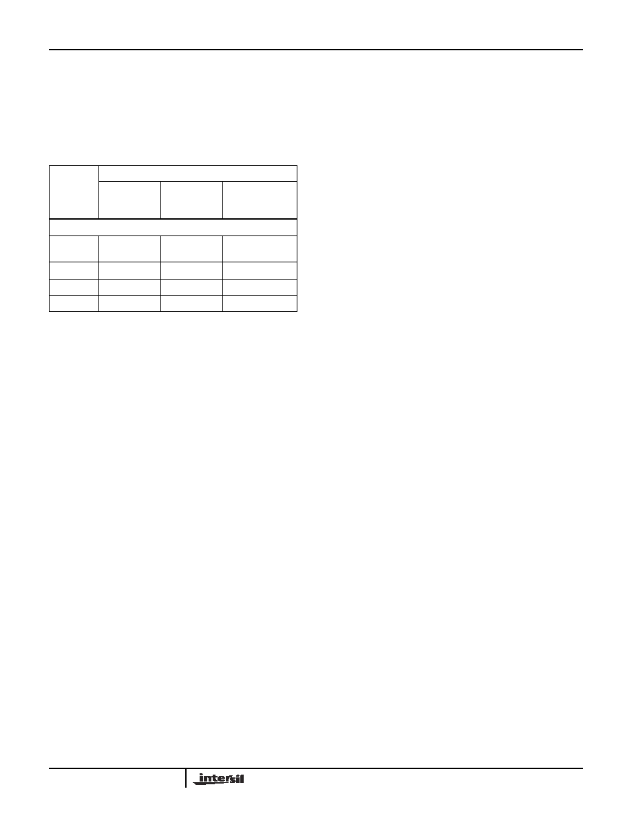
TABLE 1.
DIGITAL
INPUT
ANALOG OUTPUT
STRAIGHT
BINARY
OFFSET
BINARY
(NOTE 5)
TWO'S
COMPLEMENT
MSB...LSB
000...000
Zero
-FS
(Full Scale)
Zero
100...000
1
/
2
FS
Zero
-FS
111...111
+FS - 1 LSB
+FS - 1 LSB
Zero - 1 LSB
011...111
1/2FS - 1 LSB
Zero - 1 LSB
+FS - 1 LSB
NOTE:
5. Invert MSB with external inverter to obtain Two's Complement
Coding.
HI-565A
5
added to convert this current to a voltage. Refer to Table 2
for the voltage output case, along with Figure 1 or Figure 2.
Calibration is a two step process for each of the five output
ranges shown in Table 2. First adjust the negative full scale
(zero for unipolar ranges). This is an offset adjust which
translates the output characteristic, i.e., affects each code by
the same amount.
Next adjust positive FS. This is a gain error adjustment, which
rotates the output characteristic about the negative FS value.
For the bipolar ranges, this approach leaves an error at the
zero code, whose maximum value is the same as for integral
nonlinearity error. In general, only two values of output may
be calibrated exactly; all others must tolerate some error.
Choosing the extreme end points (plus and minus full scale)
minimizes this distributed error for all other codes.
TABLE 2. OPERATING MODES AND CALIBRATION
MODE
CIRCUIT CONNECTIONS
CALIBRATION
OUTPUT
PRANGE
PIN 10 TO
PIN 11 TO
RESlSTOR (R)
APPLY
INPUT CODE
ADJUST
TO SET
V
O
Unipolar
(See Figure 1)
0 to +10V
V
O
Pin 10
1.43K
All 0's
All 1's
R1
R2
0V
+9.99756V
0 to +5V
V
O
Pin 9
1.1K
All 0's
All 1's
R1
R2
0V
+4.99878V
Bipolar
(See Figure 2)
±
10V
NC
V
O
1.69K
All 0's
All 1's
R3
R4
-10V
+9.99512V
±
5V
V
O
Pin 10
1.43K
All 0's
All 1's
R3
R4
-5V
+4.99756V
±
2.5V
V
O
Pin 9
1.1K
All 0's
All 1's
R3
R4
-2.5V
+2.49878V
REF OUT
x CODE)
(4 x I REF
IO
3.5K
3K
CODE
INPUT
DAC
2.5K
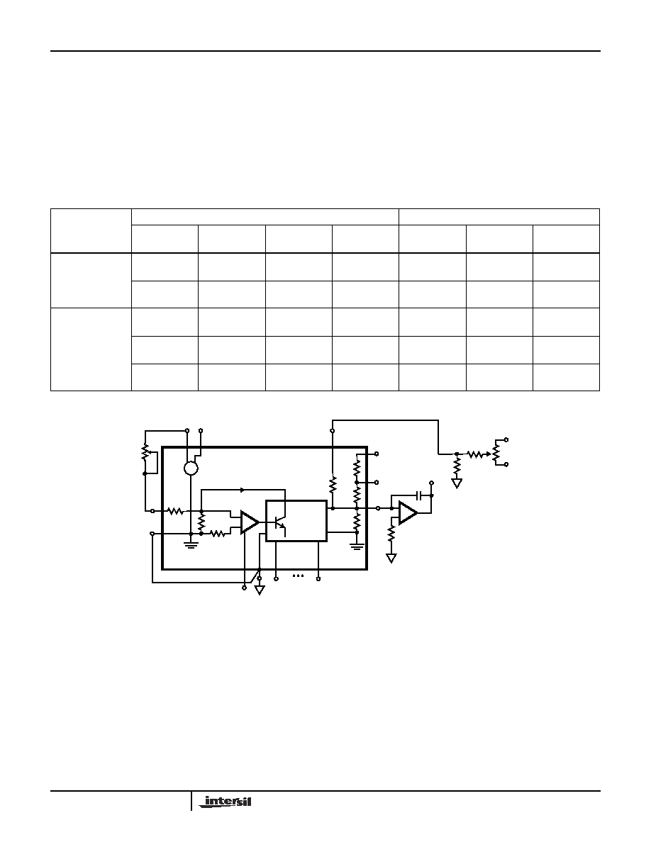
5K
9
DAC
OUT
C
9.95K
5K
10
11
20V SPAN
10V SPAN
VO
R (SEE
0.5mA
I REF
HI-565A
19.95K
+
-
4
3
6
5
8
BIP.
OFF.
VCC
7
12
24
13
MSB
LSB
REF
GND
REF
IN
10V
-V
EE
PWR
GND
R2
100
TABLE 2)
+
-
+
-
+15V
-15V
100k
100
50k
R1
FIGURE 1. UNIPOLAR VOLTAGE OUTPUT
HI-565A