HI-574A, HI-674A
1
TM
File Number
3096.5
CAUTION: These devices are sensitive to electrostatic discharge; follow proper IC Handling Procedures.
1-888-INTERSIL or 321-724-7143
|
Intersil and Design is a trademark of Intersil Americas Inc.
|
Copyright © Intersil Americas Inc. 2001
HI-574A, HI-674A
Complete, 12-Bit A/D Converters with
Microprocessor Interface
The HI-X74(A) is a complete 12-bit, Analog-to-Digital
Converter, including a +10V reference clock, three-state
outputs and a digital interface for microprocessor control.
Successive approximation conversion is performed by two
monolithic dice housed in a 28 lead package. The bipolar
analog die features the Intersil Dielectric Isolation process,
which provides enhanced AC performance and freedom
from latch-up.
Custom design of each IC (bipolar analog and CMOS digital)
has yielded improved performance over existing versions of
this converter. The voltage comparator features high PSRR
plus a high speed current-mode latch, and provides precise
decisions down to 0.1 LSB of input overdrive. More than 2X
reduction in noise has been achieved by using current
instead of voltage for transmission of all signals between the
analog and digital ICs. Also, the clock oscillator is current
controlled for excellent stability over temperature.
The HI-X74(A) offers standard unipolar and bipolar input
ranges, laser trimmed for specified linearity, gain and offset
accuracy. The low noise buried zener reference circuit is
trimmed for minimum temperature coefficient.
Power requirements are +5V and
±
12V to
±
15V, with typical
dissipation of 385mW (HI-574A/674A) at 12V.
Features
· Complete 12-Bit A/D Converter with Reference and Clock
· Full 8-Bit, 12-Bit or 16-Bit Microprocessor Bus Interface
· Bus Access Time . . . . . . . . . . . . . . . . . . . . . . . . . . . 150ns
· No Missing Codes Over Temperature
· Minimal Setup Time for Control Signals
· Fast Conversion Times
- HI-574A (Max) . . . . . . . . . . . . . . . . . . . . . . . . . . . . 25
µ
s
- HI-674A (Max) . . . . . . . . . . . . . . . . . . . . . . . . . . . . 15
µ
s
· Low Noise, via Current-Mode Signal Transmission
Between Chips
· Byte Enable/Short Cycle (A
O
Input)
- Guaranteed Break-Before-Make Action, Eliminating Bus
Contention During Read Operation. Latched by Start
Convert Input (To Set the Conversion Length)
· Supply Voltage . . . . . . . . . . . . . . . . . . . . . .
±
12V to
±
15V
Applications
· Military and Industrial Data Acquisition Systems
· Electronic Test and Scientific Instrumentation
· Process Control Systems
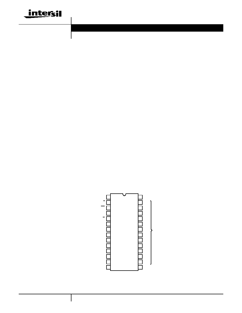
Pinout
(PDIP, SBDIP)
TOP VIEW
STATUS, STS
DB11
DB10
DB9
DB8
DB7
DB6
DB5
DB4
DB3
DB2
DB1
DB0
DIG COMMON,
DIGITAL
DATA
OUTPUTS
1
2
3
4
5
6
7
8
9
10
11
12
13
14
28
27
26
25
24
23
22
21
20
19
18
17
16
15
CHIP ENABLE, CE
+10V REF, REF OUT
REFERENCE INPUT
20V INPUT
ANALOG
COMMON, AC
+12V/+15V SUPPLY, V
CC
BYTE ADDR/SHORT
CYCLE, A
O
10V INPUT
+5V SUPPLY, V
LOGIC
CHIP SEL, CS
DATA MODE SEL, 12/8
READ/CONVERT, R/C
BIPOLAR OFFSET
BIP OFF
-12V/-15V SUPPLY, V
EE
MSB
LSB
DC
Data Sheet
June 2001
itle
I-
4A,
-
4A,
-
4)
bjec
omp
e,
-Bit
D
nver
s
th
crop
esso
erfa
utho
)
eyw
s
tersi
rpor
on,
ico
ucto
/D,
C,
sh,
nver
, bit,
le
dem
2
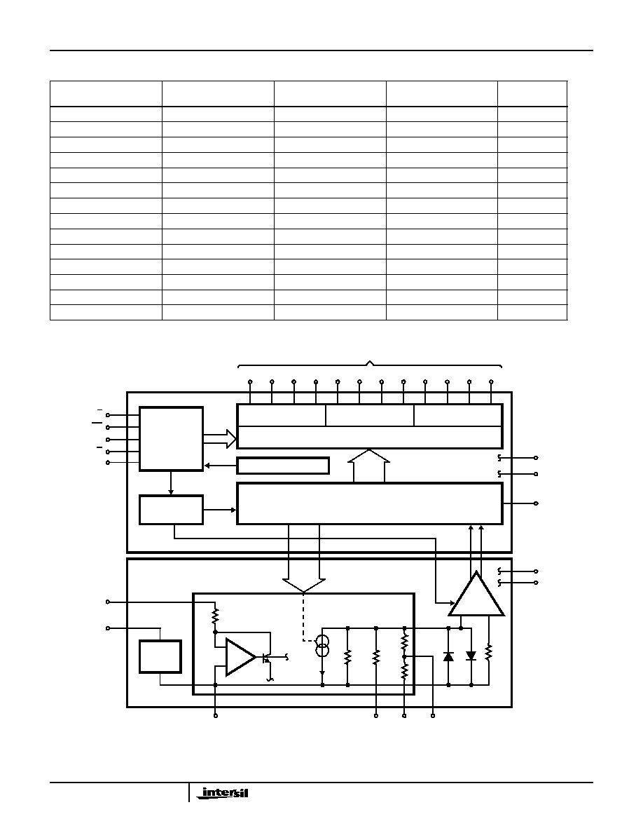
Functional Block Diagram
Ordering Information
PART NUMBER
INL
TEMPERATURE RANGE
(
o
C)
PACKAGE
PKG. NO.
HI3-574AJN-5
±
1.0 LSB
0 to 75
28 Ld PDIP
E28.6
HI3-574AKN-5
±
0.5 LSB
0 to 75
28 Ld PDIP
E28.6
HI1-574AJD-5
±
1.0 LSB
0 to 75
28 Ld SBDIP
D28.6
HI1-574AKD-5
±
0.5 LSB
0 to 75
28 Ld SBDIP
D28.6
HI1-574ASD-2
±
1.0 LSB
-55 to 125
28 Ld SBDIP
D28.6
HI1-574ATD-2
±
0.5 LSB
-55 to 125
28 Ld SBDIP
D28.6
HI1-574ASD/883
±
1.0 LSB
-55 to 125
28 Ld SBDIP
D28.6
HI1-574ATD/883
±
0.5 LSB
-55 to 125
28 Ld SBDIP
D28.6
HI3-674AJN-5
±
1.0 LSB
0 to 75
28 Ld PDIP
E28.6
HI3-674AKN-5
±
0.5 LSB
0 to 75
28 Ld PDIP
E28.6
HI1-674AJD-5
±
1.0 LSB
0 to 75
28 Ld SBDIP
D28.6
HI1-674AKD-5
±
0.5 LSB
0 to 75
28 Ld SBDIP
D28.6
HI1-674ASD-2
±
1.0 LSB
-55 to 125
28 Ld SBDIP
D28.6
HI1-674ATD/883
±
0.5 LSB
-55 to 125
28 Ld SBDIP
D28.6
BIT OUTPUTS
MSB
LSB
NIBBLE B (NOTE)
NIBBLE C (NOTE)
NIBBLE A (NOTE)
POWER-UP RESET
THREE-STATE BUFFERS AND CONTROL
12 BITS
SAR
STROBE
DIGITAL CHIP
CONTROL
CLK
OSCILLATOR
LOGIC
ANALOG CHIP
DAC
10K
+10V
REF
-
+
5K
5K
5K
2.5K
10V
INPUT
20V
INPUT
BIP
OFF
ANALOG
COMMON
COMP
-
+
12/8
CS
A
O
R/C
CE
V
REF
IN
V
REF
OUT
V
LOGIC
DIGITAL
COMMON
STS
V
CC
V
EE
10K
NOTE: "Nibble" is a 4-bit digital word.
12 BITS
HI-574A, HI-674A
3
Absolute Maximum Ratings
Thermal Information
Supply Voltage
V
CC
to Digital Common . . . . . . . . . . . . . . . . . . . . . . 0V to +16.5V
V
EE
to Digital Common . . . . . . . . . . . . . . . . . . . . . . . 0V to -16.5V
V
LOGIC
to Digital Common . . . . . . . . . . . . . . . . . . . . . . 0V to +7V
Analog Common to Digital Common
. . . . . . . . . . . . . . . . . . . . . . ±
1V
Control Inputs
(CE, CS, A
O
, 12/8, R/C) to Digital Common . . -0.5V to V
LOGIC
+0.5V
Analog Inputs
(REFIN, BIPOFF, 10VIN) to Analog Common . . . . . . . . . .
±
16.5V
20VIN to Analog Common . . . . . . . . . . . . . . . . . . . . . . . . . .
±
24V
REFOUT . . . . . Indefinite Short To Common, Momentary Short To V
CC
Operating Conditions
Temperature Range
HI3-574Axx-5, HI1-674Axx-5 . . . . . . . . . . . . . . . . . . . 0
o
C to 75
o
C
HI1-574AxD-2, HI1-674AxD-2 . . . . . . . . . . . . . . . -55
o
C to 125
o
C
Thermal Resistance (Typical, Note 1)
JA
(
o
C/W)
JC
(
o
C/W)
SBDIP Package. . . . . . . . . . . . . . . . . .
55
18
PDIP Package . . . . . . . . . . . . . . . . . . .
60
N/A
Maximum Junction Temperature
PDIP Package . . . . . . . . . . . . . . . . . . . . . . . . . . . . . . . . . . . 150
o
C
SBDIP Package . . . . . . . . . . . . . . . . . . . . . . . . . . . . . . . . . . 175
o
C
Maximum Storage Temperature Range
PDIP Package . . . . . . . . . . . . . . . . . . . . . . . . . . . . . -40
o
C to 85
o
C
SBDIP Package . . . . . . . . . . . . . . . . . . . . . . . . . . . -65
o
C to 150
o
C
Maximum Lead Temperature (Soldering, 10s) . . . . . . . . . . . . 300
o
C
Die Characteristics
Transistor Count
HI-574A, HI-674A . . . . . . . . . . . . . . . . . . . . . . . . . . . . . . . . . .1117
CAUTION: Stresses above those listed in "Absolute Maximum Ratings" may cause permanent damage to the device. This is a stress only rating and operation of the
device at these or any other conditions above those indicated in the operational sections of this specification is not implied.
NOTE:
1.
JA
is measured with the component mounted on a low effective thermal conductivity test board in free air. See Tech Brief TB379 for details.
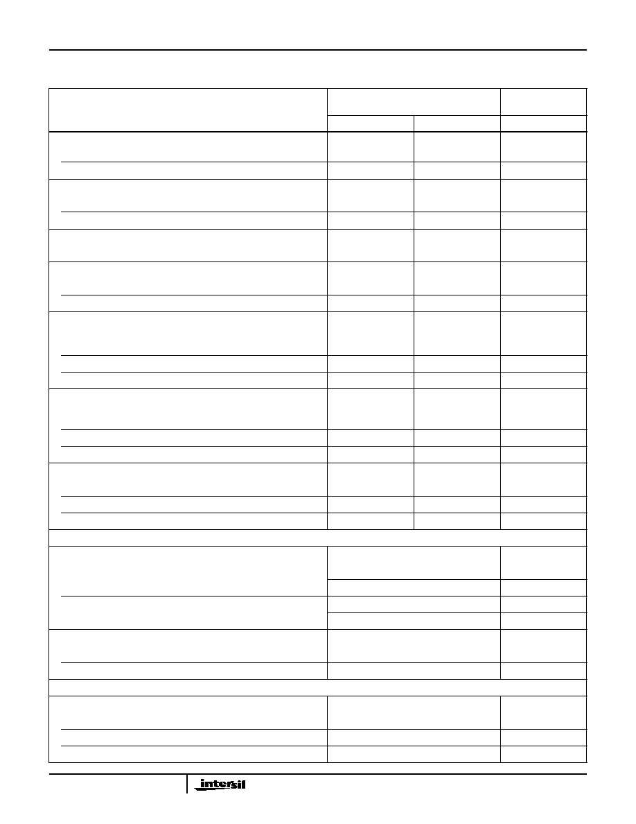
DC and Transfer Accuracy Specifications
Typical at 25
o
C with V
CC
= +15V or +12V, V
LOGIC
= +5V, V
EE
= -15V or -12V,
Unless Otherwise Specified
PARAMETER
TEMPERATURE RANGE
-5 (0
o
C to 75
o
C)
UNITS
J SUFFIX
K SUFFIX
DYNAMIC CHARACTERISTICS
Resolution (Max)
12
12
Bits
Linearity Error
25
o
C (Max)
±
1
±
1
/
2
LSB
0
o
C to 75
o
C (Max)
±
1
±
1
/
2
LSB
Max Resolution For Which No Missing Codes Is Guaranteed
25
o
C
12
12
Bits
T
MIN
to T
MAX
11
12
Bits
Unipolar Offset (Max)
Adjustable to Zero
±
2
±
1.5
LSB
Bipolar Offset (Max)
V
IN
= 0V (Adjustable to Zero)
±
4
±
4
LSB
V
IN
= -10V
±
0.15
±
0.1
% of FS
Full Scale Calibration Error
25
o
C (Max), With Fixed 50
Resistor From REF OUT To REF IN
(Adjustable to Zero)
±
0.25
±
0.25
% of FS
T
MIN
to T
MAX
(No Adjustment At 25
o
C)
±
0.475
±
0.375
% of FS
T
MIN
to T
MAX
(With Adjustment To Zero 25
o
C)
±
0.22
±
0.12
% of FS
Temperature Coefficients
Guaranteed Max Change, T
MIN
to T
MAX
(Using Internal Reference)
Unipolar Offset
±
2
±
1
LSB
Bipolar Offset
±
2
±
1
LSB
Full Scale Calibration
±
9
±
2
LSB
HI-574A, HI-674A
4
8
Power Supply Rejection Max Change In Full Scale Calibration
+13.5V < V
CC
< +16.5V or +11.4V < V
CC
< +12.6V
±
2
±
1
LSB
+4.5V < V
LOGIC
< +5.5V
±
1
/
2
±
1
/
2
LSB
-16.5V < V
EE
< -13.5V or -12.6V < V
EE
< -11.4V
±
2
±
1
LSB
ANALOG INPUTS
Input Ranges
Bipolar
-5 to +5 (Note 3)
V
-10 to +10 (Note 4)
V
Unipolar
0 to +10 (Note 3)
V
0 to +20 (Note 4)
V
Input Impedance
10V Span
5K,
±
25%
20V Span
10K,
±
25%
POWER SUPPLIES
Operating Voltage Range
V
LOGIC
+4.5 to +5.5
V
V
CC
+11.4 to +16.5
V
V
EE
-11.4 to -16.5
V
Operating Current
I
LOGIC
7 Typ, 15 Max
mA
I
CC
+15V Supply
11 Typ, 15 Max
mA
I
EE
-15V Supply
21 Typ, 28 Max
mA
Power Dissipation
±
15V, +5V
515 Typ, 720 Max
mW
±
12V, +5V
385 Typ
mW
Internal Reference Voltage
T
MIN
to T
MAX
+10.00
±
0.05 Max
V
Output Current, Available For External Loads (External Load Should Not
Change During Conversion).
2.0 Max
mA
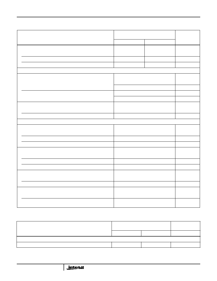
DC and Transfer Accuracy Specifications
Typical at 25
o
C with V
CC
= +15V or +12V, V
LOGIC
= +5V, V
EE
= -15V or -12V,
Unless Otherwise Specified (Continued)
PARAMETER
TEMPERATURE RANGE
-2 (-55
o
C to 125
o
C)
S SUFFIX
T SUFFIX
UNITS
DYNAMIC CHARACTERISTICS
Resolution (Max)
12
12
Bits
DC and Transfer Accuracy Specifications
Typical at 25
o
C with V
CC
= +15V or +12V, V
LOGIC
= +5V, V
EE
= -15V or -12V,
Unless Otherwise Specified (Continued)
PARAMETER
TEMPERATURE RANGE
-5 (0
o
C to 75
o
C)
UNITS
J SUFFIX
K SUFFIX
HI-574A, HI-674A
5
Linearity Error
25
o
C
±
1
±
1
/
2
LSB
-55
o
C to 125
o
C (Max)
±
1
±
1
LSB
Max Resolution For Which No Missing Codes Is Guaranteed
25
o
C
12
12
Bits
T
MIN
to T
MAX
11
12
Bits
Unipolar Offset (Max)
Adjustable to Zero
±
2
±
1.5
LSB
Bipolar Offset (Max)
V
IN
= 0V (Adjustable to Zero)
±
4
±
4
LSB
V
IN
= -10V
±
0.15
±
0.1
% of FS
Full Scale Calibration Error
25
o
C (Max), With Fixed 50
Resistor From REF OUT To REF IN
(Adjustable To Zero)
±
0.25
±
0.25
% of FS
T
MIN
to T
MAX
(No Adjustment At 25
o
C)
±
0.75
±
0.50
% of FS
T
MIN
to T
MAX
(With Adjustment To Zero At 25
o
C)
±
0.50
±
0.25
% of FS
Temperature Coefficients
Guaranteed Max Change, T
MIN
to T
MAX
(Using Internal Reference)
Unipolar Offset
±
2
±
1
LSB
Bipolar Offset
±
2
±
2
LSB
Full Scale Calibration
±
20
±
10
LSB
Power Supply Rejection Max Change In Full Scale Calibration
+13.5V < V
CC
< +16.5V or +11.4V < V
CC
< +12.6V
±
2
±
1
LSB
+4.5V < V
LOGIC
< +5.5V
±
1
/
2
±
1
/
2
LSB
-16.5V < V
EE
< -13.5V or -12.6V < V
EE
< -11.4V
±
2
±
1
LSB
ANALOG INPUTS
Input Ranges
Bipolar
-5 to +5 (Note 3)
V
-10 to +10 (Note 4)
V
Unipolar
0 to +10 (Note 3)
V
0 to +20 (Note 4)
V
Input Impedance
10V Span
5K,
±
25%
20V Span
10K,
±
25%
POWER SUPPLIES
Operating Voltage Range
V
LOGIC
+4.5 to +5.5
V
V
CC
+11.4 to +16.5
V
V
EE
-11.4 to -16.5
V
DC and Transfer Accuracy Specifications
Typical at 25
o
C with V
CC
= +15V or +12V, V
LOGIC
= +5V, V
EE
= -15V or -12V,
Unless Otherwise Specified (Continued)
PARAMETER
TEMPERATURE RANGE
-2 (-55
o
C to 125
o
C)
S SUFFIX
T SUFFIX
UNITS
HI-574A, HI-674A