 | –≠–ª–µ–∫—Ç—Ä–æ–Ω–Ω—ã–π –∫–æ–º–ø–æ–Ω–µ–Ω—Ç: HI2302JCQ | –°–∫–∞—á–∞—Ç—å:  PDF PDF  ZIP ZIP |
4-1
November 1997
HI2302
8-Bit, 50 MSPS, Video
A/D Converter with Clamp Function
Features
∑ Resolution . . . . . . . . . . . . . . . . . . 8-Bit
±
0.5 LSB (DNL)
∑ Maximum Sampling Frequency . . . . . . . . . . . 50 MSPS
∑ Low Power Consumption . . . . . . . . . . . . . . . . . .125mW
(Reference Current Excluded)
∑ Built-In Input Clamp Function (DC Restore)
∑ Clamp ON/OFF Function
∑ Internal Voltage Reference
∑ Input CMOS/TTL Compatible
∑ Three-State TTL Compatible Output
∑ Power Supply . . . . . . . . . . . . . . . . . . . . . . . . . +5V Single
or +5V/3.3V Dual
∑ Direct Replacement for Sony CXD2302Q
Applications
∑ Video Digitizing
∑ Wireless Receivers
∑ LCD Projectors/Panels
∑ Cable Modems
∑ RGB Graphics Processing
∑ Camcorders
∑ Instrumentation
Description
The HI2302 is an 8-bit CMOS A/D Converter for video with
synchronizing clamp function. The adoption of two-step
parallel method achieves low power consumption and a
maximum conversion rate of 50 MSPS. For pin compatible
lower sample rate converters refer to HI1179 (35 MSPS) or
HI1176 (20 MSPS) data sheets.
Pinout
HI2302 (MQFP)
TOP VIEW
Ordering Information
PART
NUMBER
TEMP.
RANGE (
o
C)
PACKAGE
PKG. NO.
HI2302JCQ
-40 to 85
32 Ld MQFP
Q32.7x7-S
AV
DD
CLP
NC
NC
CLK
TEST
DV
DD
TEST
V
RBS
V
REF
CCP
DV
SS
CLE
OE
DV
SS
NC
D0
D1
D2
D3
D4
D5
D6
D7
V
RB
AV
SS
AV
SS
V
IN
AV
DD
AV
DD
V
RT
V
RTS
1
2
3
4
5
6
7
8
16
15
14
13
12
11
10
9
17
18
19
20
21
22
23
24
32 31 30 29 28 27 26 25
File Number
4105.1
CAUTION: These devices are sensitive to electrostatic discharge; follow proper IC Handling Procedures.
1-888-INTERSIL or 321-724-7143 | Copyright © Intersil Corporation 1999
4-2
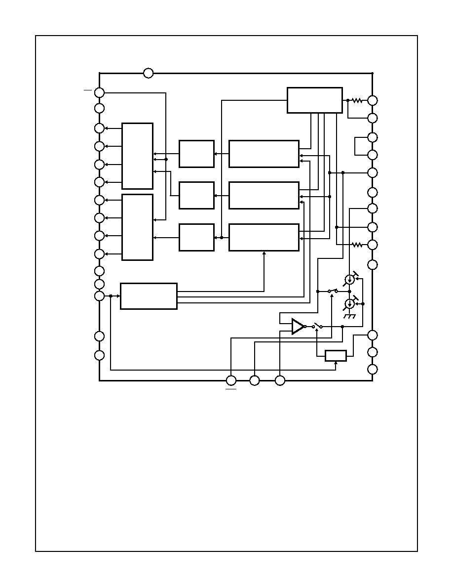
Functional Block Diagram
+
-
LOWER
SAMPLING COMPARATOR
(4-BIT)
LOWER
SAMPLING COMPARATOR
(4-BIT)
UPPER
SAMPLING COMPARATOR
(4-BIT)
LOWER
ENCODER
(4-BIT)
LOWER
ENCODER
(4-BIT)
UPPER
ENCODER
(4-BIT)
LOWER
DATA
LATCH
UPPER
DATA
LATCH
CLOCK GENERATOR
30
31
2
3
4
5
6
7
8
10
11
12
REFERENCE
SUPPLY
29
27
26
D-FF
28
25
24
23
22
21
20
19
18
17
16
15
14
13
V
RTS
AV
DD
V
RT
AV
DD
V
IN
AV
SS
AV
SS
V
RB
V
RBS
AV
DD
CLP
NC
NC
V
REF
CCP
CLE
9
32
NC
TEST (OPEN)
CLK
TEST (OPEN)
DV
DD
D7 (MSB)
D6
D5
D4
D3
D2
D1
D0 (LSB)
DV
SS
OE
DV
SS
1
HI2302
4-3
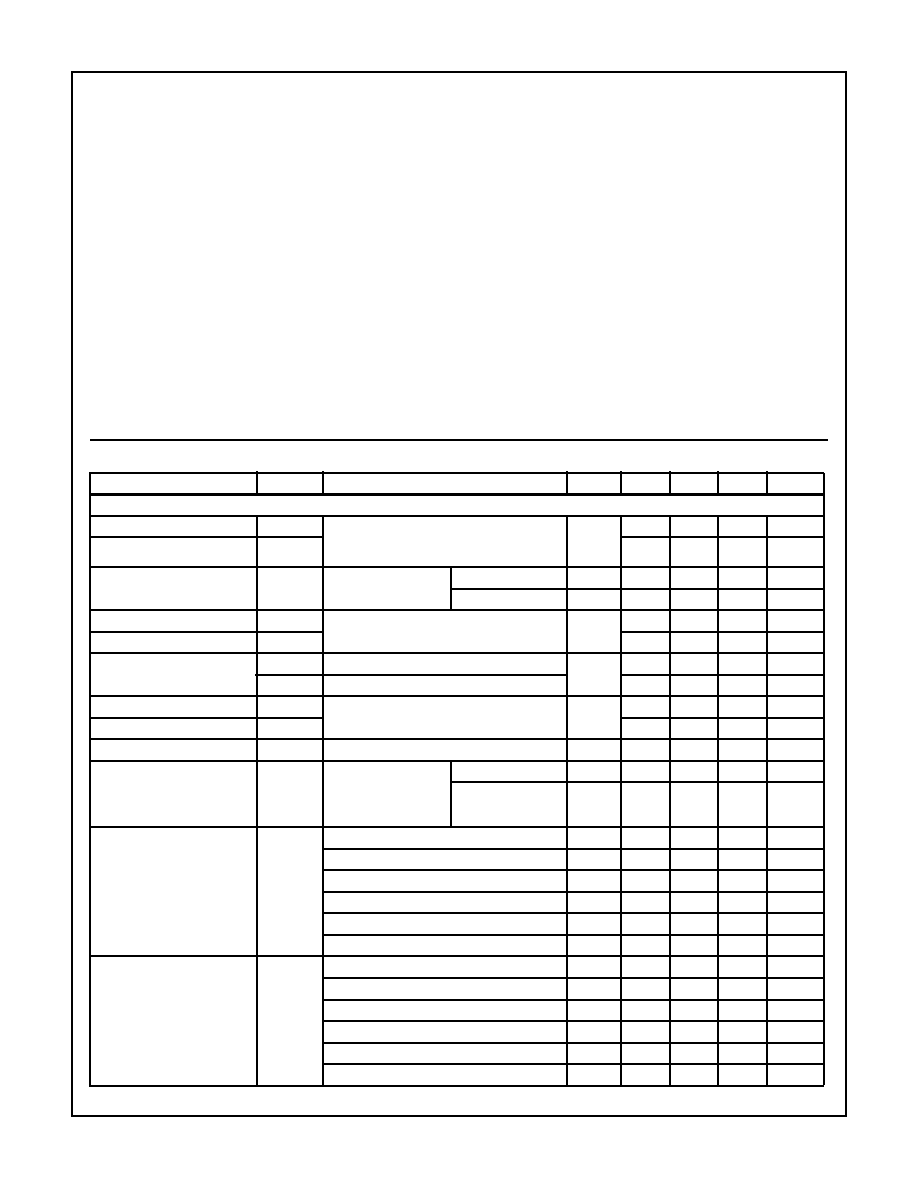
Absolute Maximum Ratings
T
A
= 25
o
C
Thermal Information
Supply Voltage (V
DD
) . . . . . . . . . . . . . . . . . . . . . . . . . . . . . . . . . . 7V
Reference Voltage (V
RT
, V
RB
) . . . . . . . . . . . V
DD
+0.5 to V
SS
-0.5V
Input Voltage (Analog) (V
IN
) . . . . . . . . . . . . . V
DD
+0.5 to V
SS
-0.5V
Input Voltage (Digital) (V
I
). . . . . . . . . . . . . . . V
DD
+0.5 to V
SS
-0.5V
Output Voltage (Digital) (V
O
) . . . . . . . . . . . . V
DD
+0.5 to V
SS
-0.5V
Operating Conditions
Supply Voltage
(AV
DD
, AV
SS
). . . . . . . . . . . . . . . . . . 4.75 to 5.25V
(DV
DD
, DV
SS
) . . . . . . . . . . . . . . . . . . . 3.0 to 5.5V
(
DV
SS
-AV
SS
) . . . . . . . . . . . . . . . . . 0 to 100mV
Reference Input Voltage
(V
RB
) . . . . . . . . . . . . . . . . . . . . . . . 0 and Above V
(V
RT
) . . . . . . . . . . . . . . . . . . . . . 2.7 and Below V
Analog Input
(V
IN
) . . . . . . . . . . . . . . . . . . . . . . . 1.7V
P-P
Above
Clock Pulse Width (t
PW1
, t
PW0
). . . . . . . . . . . . . . . . . . . . 10ns (Min)
Ambient Temperature (T
OPR
). . . . . . . . . . . . . . . . . . . -40
o
C to 85
o
C
Thermal Resistance (Typical, Note 1)
JA
(
o
C/W)
MQFP Package . . . . . . . . . . . . . . . . . . . . . . . . . . . .
122
Maximum Junction Temperature (Plastic Package) . . . . . . . . 150
o
C
Maximum Storage Temperature Range . . . . . . . . . .-55
o
C to 150
o
C
Maximum Lead Temperature (Soldering 10s) . . . . . . . . . . . . . 300
o
C
(MQFP - Lead Tips Only)
CAUTION: Stresses above those listed in "Absolute Maximum Ratings" may cause permanent damage to the device. This is a stress only rating and operation
of the device at these or any other conditions above those indicated in the operational sections of this specification is not implied.
NOTE:
1.
JA
is measured with the component mounted on an evaluation PC board in free air.
Electrical Specifications
f
C
= 50 MSPS, AV
DD
= 5V, DV
DD
= 3 to 5.5V, V
RB
= 0.5V, V
RT
= 2.5V, T
A
= 25
o
C
PARAMETER
SYMBOL
TEST CONDITIONS
NOTES
MIN
TYP
MAX
UNITS
ANALOG CHARACTERISTICS
Maximum Conversion Rate
f
C
Max
AV
DD
= 4.75 to 5.25V, T
A
= 20 to 75
o
C, V
IN
= 0.5 to 2.5V,
f
IN
= 1kHz Triangular Wave
50
65
-
MSPS
Minimum Conversion Rate
f
C
Min
-
-
0.5
MSPS
Input Bandwidth Full Scale
BW
Envelope
R
IN
= 33
-1dB
-
60
-
MHz
-3dB
-
100
-
MHz
Differential Nonlinearity Error
E
D
End Point
-
±
0.3
0.5
LSB
Integral Nonlinearity Error
E
L
-
+0.7
1.5
LSB
Offset Voltage
E
OT
Potential Difference to V
RT
Note 2
-70
-50
-30
mV
E
OB
Potential Difference to V
RB
20
40
60
mV
Differential Gain Error
DG
NTSC 40 IRE Mod Ramp
f
C
= 14.3 MSPS
-
3
-
%
Differential Phase Error
DP
-
1.5
-
Degrees
Sampling Delay
t
SD
-
0
-
ns
Clamp Offset Voltage
E
OC
V
IN
= DC, C
IN
= 10
µ
F
t
PCW
= 2.75
µ
s,
f
C
= 14.3 MSPS,
f
CLP
= 15.75kHz
V
REF
= 0.5V
0
20
40
mV
V
REF
= 2.5V
0
20
40
mV
Signal-To-Noise Ratio
SNR
f
IN
= 100kHz
-
45
-
dB
f
IN
= 500kHz
-
44
-
dB
f
IN
= 1MHz
-
44
-
dB
f
IN
= 3MHz
-
43
-
dB
f
IN
= 10MHz
-
38
-
dB
f
IN
= 25MHz
-
32
-
dB
Spurious Free Dynamic
SFDR
f
IN
= 100kHz
-
51
-
dB
f
IN
= 500kHz
-
46
-
dB
f
IN
= 1MHz
-
49
-
dB
f
IN
= 3MHz
-
46
-
dB
f
IN
= 10MHz
-
45
-
dB
f
IN
= 25MHz
-
45
-
dB
HI2302

4-4
DC CHARACTERISTICS
f
C
= 50 MSPS, AV
DD
= 5V, DV
DD
= 5V or 3.3V, V
RB
= 0.5V, V
RT
= 2.5V, T
A
= 25
o
C
Supply Current
I
AD
+ I
DD
NTSC Ramp,
Wave Input,
CLE = 0V
DV
DD
= 5V
-
25
36
mA
Analog
I
AD
DV
DD
= 3.3V
-
23
33
mA
Digital
I
DD
-
2
3
mA
Reference Current
I
REF
4.1
5.4
7.7
mA
Reference Resistance
(V
RT
- V
RB
)
R
REF
260
370
480
Self-Bias Voltage
V
RB
Shorts V
RTS
and A
VDD
Shorts V
RBS
and A
VSS
0.52
0.56
0.60
V
V
RT -
V
RB
1.80
1.92
2.04
V
Input Capacitance
C
AI1
V
IN
, V
IN
= 1.5V + 0.07V
RMS
-
15
-
pF
C
AI2
V
RTS
, V
RT
, V
RB
, V
RBS
, V
REF
-
-
11
pF
C
DIN
TEST, CLK, CLP, CLE, OE
-
-
11
pF
Output Capacitance
C
AO
CCP
-
-
11
pF
C
DO
D0 to D7, TEST
-
-
11
pF
Digital Input Voltage
V
IH
AV
DD
= 4.75 to 5.25V,
DV
DD
= 3 to 5.5V, T
A
= -20
o
C to 75
o
C
2.2
-
-
V
V
IL
-
-
0.8
V
Digital Input Current
I
IH
I
IL
V
I
= 0V to AV
DD
,
T
A
= 20
o
C to 75
o
C
CLK
-240
-
240
µ
A
TEST, CLP, CLE
-240
-
40
µ
A
OE
-40
-
240
µ
A
Digital Output Current
I
OH
OE = 0V, DV
DD
= 5V
T
A
= 20
o
C to 75
o
C
V
OH
= DV
DD
- 0.8V
-
-
-2
mA
I
OL
V
OL
= 0.4V
4
-
-
mA
I
OH
OE = 0V
DV
DD
= 3.3V
T
A
= -20
o
C to 75
o
C
V
OH
= DV
DD
- 0.8V
-
-
-1.2
mA
I
OL
V
OL
= 0.4V
2.4
-
-
mA
I
OZH
OE = 3V
DV
DD
= 3 to 5.5V
T
A
= -20
o
C to 75
o
C
V
OH
= DV
DD
-40
-
40
µ
A
I
OZL
V
OL
= 0V
-40
-
40
µ
A
TIMING
f
C
= 50 MSPS, AV
DD
= 5V, DV
DD
= 5V or 3.3V, V
RB
= 0.5V, V
RT
= 2.5V, T
A
= 25
o
C
Output Data Delay
t
PZH
CL = 15pF
OE = 0V
DV
DD
= 5V
5.5
9.5
12.0
ns
t
PHL
8.5
ns
t
PLH
DV
DD
= 3.3V
4.3
11.8
16.3
ns
t
PHL
7.6
ns
Three-State Output Enable
Time
t
PZH
R
L
= 1k
C
L
= 15pF
OE = 3V
0V
DV
DD
= 5V
2.5
4.5
8.0
ns
t
PZL
6.0
ns
t
PZH
DV
DD
= 3.3V
3.0
7.0
9.0
ns
t
PZL
5.0
ns
Three-State Output Enable
Time
t
PHZ
, t
PLZ
R
L
= 1k
, C
L
= 15pF
OE = 3V
0V
DV
DD
= 5V
3.5
5.5
7.5
ns
t
PZH
, t
PZL
DV
DD
= 3.3V
2.5
5.5
8.0
ns
Clamp Pulse Width
t
CPW
f
C
= 14.3MHz, C
IN
= 10
µ
F for NTSC Wave
Note 4
1.75
2.75
3.75
µ
s
NOTES:
2. The offset voltage E
OB
is a potential difference between V
RB
and a point of position where the voltage drops equivalent to
1
/
2
LSB of
the voltage when the output data changes from "00000000" to "00000001". E
OT
is a potential difference between V
RT
and a potential
point where the voltage rises equivalent to
1
/
2
LSB of the voltage when the output data changes from "11111111" to "11111110".
3. The voltage of up to (AV
DD
+ 0.5V) can be input when DV
DD
= 3.3V. But the output pin voltage is less than the DV
DD
voltage. When the
digital output is in the high impedance mode, the IC may be damaged by applying the voltage which is more than the (DV
DD
+ 0.5V)
voltage to the digital output.
4. The clamp pulse width is for NTSC as an example. Adjust the rate to the clamp pulse cycle (1/15.75kHz for NTSC) for other processing
systems to equal the values for NTSC.
Electrical Specifications
f
C
= 50 MSPS, AV
DD
= 5V, DV
DD
= 3 to 5.5V, V
RB
= 0.5V, V
RT
= 2.5V, T
A
= 25
o
C (Continued)
PARAMETER
SYMBOL
TEST CONDITIONS
NOTES
MIN
TYP
MAX
UNITS
HI2302
4-5
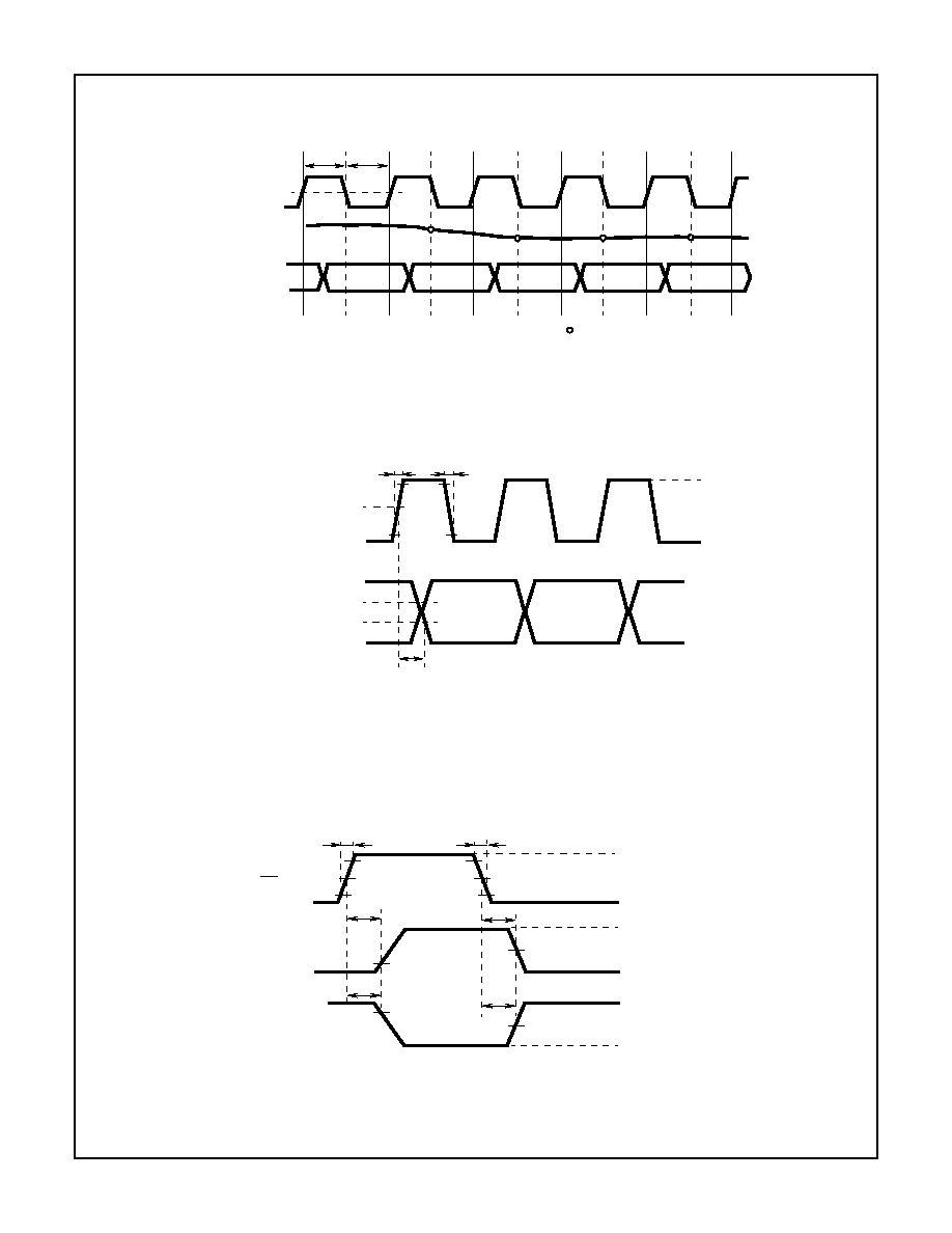
Timing Diagrams
FIGURE 1A. TIMING CHART
FIGURE 1B. TIMING CHART
FIGURE 1C. TIMING CHART
= ANALOG SIGNAL SAMPLING POINT
N + 1
N + 4
N + 3
N
N - 1
N + 2
N + 1
N - 2
N - 3
N
t
PW1
t
PW0
CLOCK 1.3V
ANALOG INPUT
DATA OUTPUT
t
r
4ns
t
f
4ns
1.3V
0.7 DV
DD
0.3 DV
DD
DATA OUTPUT
t
PLH,
t
PHL
CLOCK
90%
10%
3V
0V
t
r
= 4.5ns
t
f
= 4.5ns
OE INPUT
OUTPUT 1
OUTPUT 2
1.3V
t
PLZ
10%
90%
t
PHZ
t
PZH
1.3V
1.3V
t
PZL
10%
90%
3V
0V
V
OH
V
OL
(
DV
SS
)
V
OH
(
DV
DD
)
V
OL
HI2302