1
File Number
4754
CAUTION: These devices are sensitive to electrostatic discharge; follow proper IC Handling Procedures.
http://www.intersil.com or 407-727-9207 | Copyright © Intersil Corporation 1999
HI-390
CMOS Analog Switch
The Hl-390 switch is a monolithic device fabricated using
CMOS technology and the Intersil dielectric isolation process.
This device is TTL compatible and features low leakage and
supply currents, low and nearly constant ON resistance over
the analog signal range, break-before-make switching and
low power dissipation.
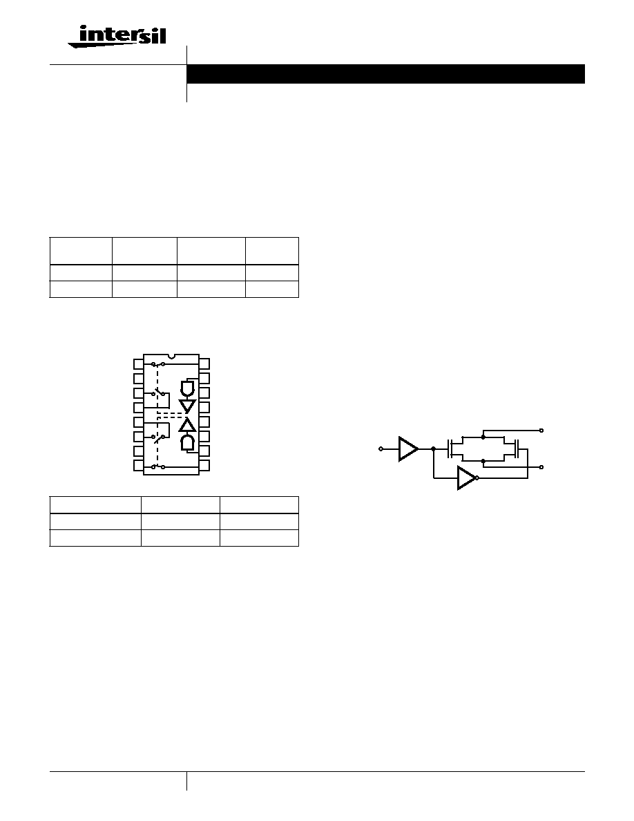
Pinout
Switch States shown for a Logic "1" Input
DUAL SPDT HI-390 (CERDIP, PDIP)
TOP VIEW
Features
∑ Analog Signal Range (
±
15V Supplies) . . . . . . . . . . .
±
15V
∑ Low Leakage . . . . . . . . . . . . . . . . . . . . . . . . . . . . . . 40pA
∑ Low On Resistance . . . . . . . . . . . . . . . . . . . . . . . . . . 35
∑ Break-Before-Make Delay . . . . . . . . . . . . . . . . . . . . 60ns
∑ Charge Injection . . . . . . . . . . . . . . . . . . . . . . . . . . . . 30pC
∑ TTL Compatible
∑ Symmetrical Switch Elements
∑ Low Operating Power . . . . . . . . . . . . . . . . . . . . . . . 1.0mW
Applications
∑ Sample and Hold (i.e., Low Leakage Switching)
∑ Op Amp Gain Switching (i.e., Low On Resistance)
∑ Portable, Battery Operated Circuits
∑ Low Level Switching Circuits
∑ Dual or Single Supply Systems
Functional Diagram
Ordering Information
PART
NUMBER
TEMP. RANGE
(
o
C)
PACKAGE
PKG. NO.
HI1-0390-2
-55 to 125
16 Ld CERDIP
F16.3
HI3-0390-5
0 to 75
16 Ld PDIP
E16.3
LOGIC
SW1, SW2
SW3, SW4
0
OFF
ON
1
ON
OFF
14
15
16
9
13
12
11
10
1
2
3
4
5
7
6
8
D
1
NC
D
3
S
3
S
4
D
4
D
2
NC
S
1
V-
GND
NC
V+
IN
2
S
2
IN
1
S
N
IN
P
D
Data Sheet
July 1999

2
Schematic Diagrams
SWITCH CELL
DIGITAL INPUT BUFFER AND LEVEL SHIFTER
MN2B
IN
MN3B
A
MP4B
MP3B
MP2B
MN4B
MP5B
V+
MN5B
V-
OUT
MP1B
A
MN1B
MP3A
MN3A
MP4A
MN4A
MP2A
MN2A
MP1A
MN1A
D2A
200
V+
LOGIC
GND
V-
IN
MP5A
MN5A
MP6A
MN6A
MP7A
MN7A
MP8A
MN8A
A
A
SWITCH CELL DRIVER
(ONE PER SWITCH CELL)
D1A
HI-390

3
Absolute Maximum Ratings
Thermal Information
Voltage Between Supplies (V+ to V-) . . . . . . . . . . . . . . . . . . . . . 44V
Digital Input Voltage . . . . . . . . . . . . . . . . . . . . . . (V+) +4V to (V-) -4V
Analog Input Voltage . . . . . . . . . . . . . . . . . . (V+) +1.5V to (V-) -1.5V
Operating Conditions
Temperature Ranges
HI-390-2 . . . . . . . . . . . . . . . . . . . . . . . . . . . . . . . . -55
o
C to 125
o
C
HI-390-5 . . . . . . . . . . . . . . . . . . . . . . . . . . . . . . . . . . . 0
o
C to 75
o
C
Thermal Resistance (Typical, Note 1)
JA
(
o
C/W)
JC
(
o
C/W)
CERDIP Package . . . . . . . . . . . . . . . . .
90
36
PDIP Package . . . . . . . . . . . . . . . . . . .
95
N/A
Maximum Junction Temperature
Hermetic Package . . . . . . . . . . . . . . . . . . . . . . . . . . . . . . . 175
o
C
Plastic Package . . . . . . . . . . . . . . . . . . . . . . . . . . . . . . . . . 150
o
C
Maximum Storage Temperature Range . . . . . . . . . . -65
o
C to 150
o
C
Maximum Lead Temperature (Soldering 10s) . . . . . . . . . . . . 300
o
C
CAUTION: Stresses above those listed in "Absolute Maximum Ratings" may cause permanent damage to the device. This is a stress only rating and operation of the
device at these or any other conditions above those indicated in the operational sections of this specification is not implied.
NOTE:
1.
JA
is measured with the component mounted on an evaluation PC board in free air.
Electrical Specifications
Supplies = +15V, -15V; V
IN
= Logic Input. V
IN
for Logic "1" = 4V, for Logic "0" = 0.8V,
Unless Otherwise Specified
PARAMETER
TEST CONDITIONS
TEMP
(
o
C)
-2
-5
UNITS
MIN
TYP
MAX
MIN
TYP
MAX
DYNAMIC CHARACTERISTICS
Switch ON Time, t
ON
25
-
210
300
-
210
300
ns
Switch OFF Time, t
OFF
25
-
160
250
-
160
250
ns
Break-Before-Make Delay, t
OPEN
25
-
60
-
-
60
-
ns
Charge Injection Voltage,
V
(Note 7)
25
-
3
-
-
3
-
mV
OFF Isolation
(Note 6)
25
-
60
-
-
60
-
dB
Input Switch Capacitance, C
S(OFF)
25
-
16
-
-
16
-
pF
Output Switch Capacitance, C
D(OFF)
25
-
14
-
-
14
-
pF
Output Switch Capacitance, C
D(ON)
25
-
35
-
-
35
-
pF
Digital Input Capacitance, C
IN
25
-
5
-
-
5
-
pF
DIGITAL INPUT CHARACTERISTICS
Input Low Level, V
INL
Full
-
-
0.8
-
-
0.8
V
Input High Level, V
INH
Full
4
-
-
4
-
-
V
Input Leakage Current (Low), I
INL
(Note 5)
Full
-
-
1
-
-
1
µ
A
Input Leakage Current (High), I
INH
(Note 5)
Full
-
-
1
-
-
1
µ
A
ANALOG SWITCH CHARACTERISTICS
Analog Signal Range
Full
-15
-
+15
-15
-
+15
V
ON Resistance, r
ON
(Note 2)
25
-
35
50
-
35
50
Full
-
40
75
-
45
75
OFF Input Leakage Current, I
S(OFF)
(Note 3)
25
-
0.04
1
-
0.04
5
nA
Full
-
1
100
-
0.2
100
nA
OFF Output Leakage Current, I
D(OFF)
(Note 3)
25
-
0.04
1
-
0.04
5
nA
Full
-
1
100
-
0.2
100
nA
ON Input Leakage Current, I
S(ON)
(Note 4)
25
-
0.03
1
-
0.03
5
nA
Full
-
0.5
100
-
0.2
100
nA
HI-390

4
POWER SUPPLY CHARACTERISTICS
Current, I+
(Note 8)
25
-
0.09
0.5
-
0.09
0.5
mA
Full
-
-
1
-
-
1
mA
Current, I-
(Note 8)
25
-
0.01
10
-
0.01
100
µ
A
Full
-
-
100
-
-
-
µ
A
Current, I+
(Note 9)
25
-
0.01
10
-
0.01
100
µ
A
Full
-
-
100
-
-
-
µ
A
Current, I-
(Note 9)
25
-
0.01
10
-
0.01
100
µ
A
Full
-
-
100
-
-
-
µ
A
NOTES:
2. V
S
=
±
10V, I
OUT
=
10mA. On resistance derived from the voltage measured across the switch under these conditions.
3. V
S
=
±
14V, V
D
=
14V.
4. V
S
= V
D
=
±
14V.
5. The digital inputs are diode protected MOS gates and typical leakages of 1nA or less can be expected.
6. V
S
= 1V
RMS
, f = 500kHz, C
L
= 15pF, R
L
= 1K, C
L
= C
FIXTURE
+ C
PROBE
, OFF Isolation = 20 Log V
S
/V
D
.
7. V
S
= 0V, C
L
= 10nF, Logic Drive = 5V pulse. Switches are symmetrical; S and D may be interchanged. Charge Injection = Q = C
L
x
V.
8. V
IN
= 4V (one input, all other inputs = 0V).
9. V
IN
= 0.8V (all inputs).
Electrical Specifications
Supplies = +15V, -15V; V
IN
= Logic Input. V
IN
for Logic "1" = 4V, for Logic "0" = 0.8V,
Unless Otherwise Specified (Continued)
PARAMETER
TEST CONDITIONS
TEMP
(
o
C)
-2
-5
UNITS
MIN
TYP
MAX
MIN
TYP
MAX
±
±
Test Circuits and Waveforms
FIGURE 1A. TEST CIRCUIT
FIGURE 1B. LOGIC INPUT
FIGURE 1C. V
ANALOG
= 10V
FIGURE 1D. V
ANALOG
= 5V
15V
V+
D
R
L
10k
C
L
10pF
V-
-15V
GND
V
LOGIC
V
GEN
R
GEN
= 0
S
IN
TIME (
µ
s)
6
4
2
0
0
0.4
0.8
1.2
1.6
LOGIC INPUT (V)
LOGIC INPUT
TIME (
µ
s)
10
5
0
0
0.4
0.8
1.2
1.6
OUTPUT V
O
L
T
A
GE (V)
V
GEN
= 10V
(NOTE 10)
TIME (
µ
s)
5
0
0
0.4
0.8
1.2
1.6
OUTPUT V
O
L
T
A
GE (V)
V
GEN
= 5V
HI-390
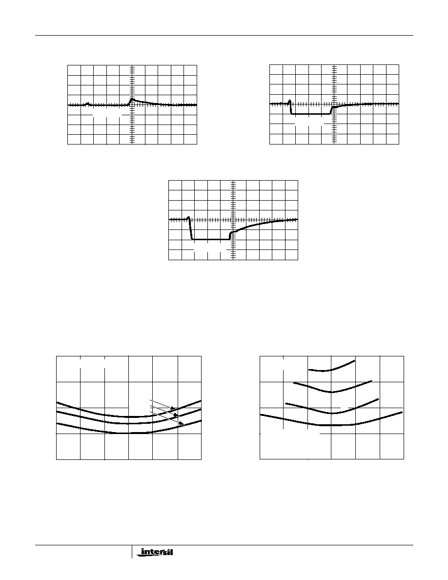
5
FIGURE 1E. V
ANALOG
= 0V
FIGURE 1F. V
ANALOG
= -5V
FIGURE 1G. V
ANALOG
= -10V
NOTE:
10. If R
GEN
, R
L
or C
L
is increased, there will be proportional increases in rise and/or fall RC times.
FIGURE 1. SWITCHING WAVEFORMS FOR VARIOUS ANALOG INPUT VOLTAGES
Test Circuits and Waveforms
(Continued)
TIME (
µ
s)
5
0
0
0.4
0.8
1.2
1.6
OUTPUT V
O
L
T
A
GE (V)
V
GEN
= 0V
-5
TIME (
µ
s)
0
0
0.4
0.8
1.2
1.6
OUTPUT V
O
L
T
A
GE (V)
V
GEN
= -5V
-5
TIME (
µ
s)
0
0
0.4
0.8
1.2
1.6
OUTPUT V
O
L
T
A
GE (V)
V
GEN
= -10V
-5
-10
Typical Performance Curves
FIGURE 2. r
DS(ON)
vs V
D
FIGURE 3. r
DS(ON)
vs V
D
DRAIN VOLTAGE (V)
r
DS(ON)
(
)
80
60
40
20
0
-15
-10
-5
0
5
10
15
V+ = +15V, V- = -15V
125
o
C
25
o
C
-55
o
C
DRAIN VOLTAGE (V)
80
60
40
20
0
-15
-10
-5
0
5
10
15
T
A
= 25
o
C
A V+ = +15V, V- = -15V
B V+ = +10V, V- = -10V
C V+ = +7.5V, V- = -7.5V
D V+ = +5V, V- = -5V
A
B
C
D
r
DS(ON)
(
)
HI-390