10-1034
Features
∑ DAC 80V/DAC 85V Alternative Source
∑ Monolithic Construction
∑ Fast Settling Time (Typ) . . . . . . . . . . . . . . . . . . . . 1.5
µ
s
∑ Guaranteed Monotonicity
∑ Wafer Laser Trimmed Linearity, Gain, Offset
∑ Span Resistors On-Chip
∑ On-Board Reference
∑ Supply Operation . . . . . . . . . . . . . . . . . . . . . . . . . .
±
12V
Applications
∑ High Speed A/D Converters
∑ Precision Instrumentation
∑ CRT Display Generation
Description
The Hl-DAC80V is a monolithic direct replacement for the
popular DAC80 and AD DAC80. The HI-DAC85V is a mono-
lithic direct replacement for the popular DAC85 and AD
DAC85 as well as the HI-5685V. Single chip construction
along with several design innovations make the Hl-DAC80V
the optimum choice for low cost, high reliability applications.
Intersil' unique Dielectric Isolation (Dl) processing reduces
internal parasitics resulting in fast switching times and mini-
mum glitch. On board span resistors are provided for good
tracking over temperature, and are laser trimmed to high
accuracy.
Internally the Hl-DAC80V/HI-DAC85V eliminates code
dependent ground currents by routing current from the posi-
tive supply to the internal ground node, as determined by an
auxiliary R2R ladder. This results in a cancellation of code
dependent ground currents allowing virtually zero variation
in current through the package common, pin 21.
The Hl-DAC80V is available as a voltage output device which
is guaranteed over the 0
o
C to 75
o
C temperature range. The
HI-DAC85V is available as a voltage output device which is
guaranteed over the -25
o
C to 85
o
C temperature range. It
includes a buried zener reference featuring a low temperature
coefficient as well as an on board operational amplifier. The
Hl-DAC80V requires only two power supplies and will operate
in the range of
±
(11.4V to 16.5V).
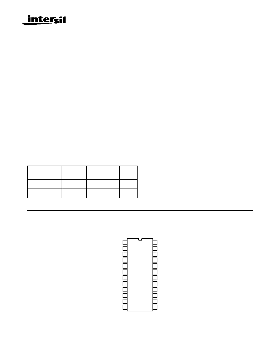
Pinout
HI-DAC80V/HI-DAC85V
(PDIP)
TOP VIEW
Ordering Information
PART NUMBER
TEMP.
RANGE (
o
C)
PACKAGE
PKG.
NO.
HI3-DAC80V-5
0 to 75
24 Ld PDIP
E24.6
HI3-DAC85V-4
-25 to 85
24 Ld PDIP
E24.6
1
2
3
4
5
6
7
8
9
10
11
12
(MSB) BIT 1
BIT 2
BIT 3
BIT 4
BIT 5
BIT 6
BIT 7
BIT 8
BIT 9
BIT 10
BIT 11
(LSB) BIT 12
16
17
18
19
20
21
22
23
24
15
14
13
6.3V REF OUT
+V
S
COMMON
JUNCTION
20V RANGE
BIPOLAR OFFSET
V
OUT
-V
S
NC
GAIN ADJUST
10V RANGE
REF INPUT
August 1997
HI-DAC80V,
HI-DAC85V
12-Bit, Low Cost, Monolithic D/A Converters
File Number
3110.1
CAUTION: These devices are sensitive to electrostatic discharge; follow proper IC Handling Procedures.
http://www.intersil.com or 407-727-9207
|
Copyright
©
Intersil Corporation 1999

10-1035
Functional Block Diagram
8K
1K
1K
8K
1K
2K
8K
1K
2K
8K
1K
2K
8K
1K
2K
8K
1K
2K
8K
1K
2K
8K
1K
2K
8K
1K
2K
8K
1K
2K
8K
8K
8K
GROUND
CURRENT
CANCEL-
LATION
CIRCUIT
+
-
V
OUT
5K
SPAN
JUNCTION
CONTROL
AMP
12.6K
8K
GAIN
ADJUST
6.3K
12.6K
BIPOLAR
OFFSET
REF
OUT
COMMON
IN
+
-
+V
S
BIT 1 IN
(MSB)
DIGITAL INPUT LEVEL SHIFTERS AND SWITCH DRIVERS
BIT 12 IN
(LSB)
5K
20V
SPAN R
10V
SPAN R
-V
S
+
-
HI-DAC80V, HI-DAC85V

10-1036
Absolute Maximum Ratings
Thermal Information
Power Supply Inputs
+V
S
. . . . . . . . . . . . . . . . . . . . . . . . . . . . . . . . . . . . . . . . . . . . +20V
-V
S
. . . . . . . . . . . . . . . . . . . . . . . . . . . . . . . . . . . . . . . . . . . . .-20V
Reference
Input (Pin 16) . . . . . . . . . . . . . . . . . . . . . . . . . . . . . . . . . . . . . +V
S
Output Drain . . . . . . . . . . . . . . . . . . . . . . . . . . . . . . . . . . . . 2.5mA
Digital Inputs (Bits 1 to 12) . . . . . . . . . . . . . . . . . . . . . . . . -1V to +V
S
Operating Conditions
Operating Temperature Range
HI-DAC80V . . . . . . . . . . . . . . . . . . . . . . . . . . . . . . . . .0
o
C to 75
o
C
HI-DAV85V . . . . . . . . . . . . . . . . . . . . . . . . . . . . . . . -25
o
C to 85
o
C
Thermal Resistance (Typical, Note 1)
JA
(
o
C/W)
PDIP Package . . . . . . . . . . . . . . . . . . . . . . . . . . . . .
60
Maximum Power Dissipation
PDIP Package . . . . . . . . . . . . . . . . . . . . . . . . . . . . . . . . . . 550mW
Maximum Junction Temperature . . . . . . . . . . . . . . . . . . . . . . . 150
o
C
Maximum Storage Temperature Range . . . . . . . . . .-65
o
C to 150
o
C
Maximum Lead Temperature (Soldering 10s) . . . . . . . . . . . . . 300
o
C
Die Characteristics
Process . . . . . . . . . . . . . . . . . . . . . . . . . . . . . . . . . . . . . . . Bipolar-DI
Transistor Count . . . . . . . . . . . . . . . . . . . . . . . . . . . . . . . . . . . . . 214
CAUTION: Stresses above those listed in "Absolute Maximum Ratings" may cause permanent damage to the device. This is a stress only rating and operation
of the device at these or any other conditions above those indicated in the operational sections of this specification is not implied.
NOTE:
1.
JA
is measured with the component mounted on an evaluation PC board in free air.
Electrical Specifications
T
A
= 25
o
C, V
S
±
12V to
±
15V (Note 4), Pin 16 to Pin 24, Unless Otherwise Specified
PARAMETER
TEST CONDITIONS
HI-DAC80V-5, HI-DAC85V-5
UNITS
MIN
TYP
MAX
SYSTEM PERFORMANCE
Resolution
-
-
12
Bits
ACCURACY (Note 2)
Linear Error
Full Temperature
-
±
1
/
4
±
1
/
2
LSB
Differential Linearity Error
Full Temperature
-
±
1
/
2
±
3
/
4
LSB
Monotonicity
Full Temperature
Guaranteed
Gain Error
Full Temperature (Notes 1, 3)
-
±
0.1
±
0.3
% FSR
Offset Error
Full Temperature (Note 1)
±
0.05
±
0.15
% FSR
ANALOG OUTPUT
Output Ranges
-
±
2.5
-
V
-
±
5
-
V
-
±
10
-
V
-
0 to 5
-
V
-
0 to 10
-
V
Output Current
±
5
-
-
mA
Output Resistance
-
0.05
-
Short Circuit Duration
To Common
Continuous
-
DRIFT (Note 2)
Total Bipolar Drift (Includes Gain,
Offset and Linearity Drifts)
Full Temperature
-
-
±
20
ppm/
o
C
Total Error
Unipolar
Full Temperature (Note 5)
-
±
0.08
±
0.15
% FSR
Bipolar
Full Temperature (Note 5)
-
±
0.06
±
0.1
% FSR
Gain
With Internal Reference
-
±
15
±
30
ppm/
o
C
Without Internal Reference
-
±
7
-
ppm/
o
C
Unipolar Offset
-
±
1
±
3
ppm/
o
C
Bipolar Offset
-
±
5
±
10
ppm/
o
C
CONVERSION SPEED
Settling Time
Full Scale Transition All Bits ON
to OFF or OFF to ON to
±
0.01%
or FSR (Note 2)
With 10K Feedback
-
3
-
µ
s
With 5K Feedback
-
1.5
-
µ
s
For 1 LSB Change
-
1.5
-
µ
s
HI-DAC80V, HI-DAC85V

10-1037
Definitions of Specifications
Digital Inputs
The Hl-DAC80V accepts digital input codes in complementary
binary, complementary offset binary, and complementary
two's complement binary.
Settling Time
That interval between application of a digital step input, and
final entry of the analog output within a specified window
about the settled value. Intersil Corporation usually specifies
a unipolar 10V full scale step, to be measured from 50% of
the input digital transition, and a window of
±
1
/
2
LSB about
the final value. The device output is then rated according to
the worst (longest settling) case: low to high, or high to low.
In a 12-bit system
±
1
/
2
LSB =
±
0.012% of FSR.
Slew Rate
10
15
-
V/
µ
s
INTERNAL REFERENCE
Output Voltage
6.250
+6.3
6.350
V
Output Impedance
-
1.5
-
External Current
-
-
+2.5
mA
Tempco of Drift
-
5
-
ppm/
o
C
DIGITAL INPUT (Note 2)
Logic Levels
Logic "1"
TTL Compatible At +1
µ
A
+2
-
+5.5
V
Logic "0"
TTL Compatible At -100
µ
A
0
-
+0.8
V
POWER SUPPLY SENSITIVITY (Notes 2, 4)
+15V Supply
-
0.001
0.002
% FSR / %V
S
-15V Supply
-
0.001
0.002
% FSR / %V
S
POWER SUPPLY CHARACTERISTICS (Note 4)
Voltage Range
+V
S
Full Temperature
+11.4
+15
+16.5
V
-V
S
Full Temperature
-11.4
-15
-16.5
V
Current
+I
S
Full Temperature, V
S
=
±
15V
-
+12
+15
mA
-I
S
Full Temperature, V
S
=
±
15V
-
-15
-20
mA
NOTES:
1. Adjustable to zero using external potentiometers.
2. See Definitions.
3. FSR is "Full Scale Range: and is 20V for
±
10V range, 10V for
±
5V range, etc.
4. The HI-DAC80V/HI-DAC85V will operate with supply voltages as low as
±
11.4V. It is recommended that output voltage range -10V to
+10V not be used if the supply voltages are less than
±
12.5V.
5. With Gain and Offset errors adjusted to zero at 25
o
C.
Electrical Specifications
T
A
= 25
o
C, V
S
±
12V to
±
15V (Note 4), Pin 16 to Pin 24, Unless Otherwise Specified (Continued)
PARAMETER
TEST CONDITIONS
HI-DAC80V-5, HI-DAC85V-5
UNITS
MIN
TYP
MAX
TABLE 1.
DIGITAL
INPUT
ANALOG OUTPUT
COMPLE-
MENTARY
STRAIGHT
BINARY
COMPLE-
MENTARY
OFFSET
BINARY
COMPLE-
MENTARY
TWO'S
COMPLEMENT
MSB...LSB
000...000
+ Full Scale
+ Full Scale
-LSB
100...000
Mid Scale-1 LSB
-1 LSB
+ Full Scale
111...111
Zero
- Full Scale
Zero
011...111
+
1
/
2
Full Scale
Zero
- Full Scale
Invert MSB with external inverter to obtain CTC Coding
HI-DAC80V, HI-DAC85V

10-1038
Thermal Drift
Thermal drift is based on measurements at 25
o
C, at high
(T
H
) and low (T
L
) temperatures. Drift calculations are made
for the high (T
H
-25
o
C) and low (25
o
C-T
L
) ranges, and the
larger of the two values is given as a specification represent-
ing worst case drift.
Gain Drift, Offset Drift, Reference Drift and Total Bipolar Drift
are calculated in parts per million per
o
C as follows:
NOTE: FSR = Full Scale Output Voltage - Zero Scale Output
Voltage
FSR = FSR (T
H
) - FSR (25
o
C),
or FSR (25
o
C) - FSR (T
L
).
V
O
= Steady State response to any input code.
Total Bipolar Drift is the variation of output voltage with
temperature, in the bipolar mode of operation. It represents
the net effect of drift in Gain, Offset, Linearity and Reference
Voltage. Total Bipolar Drift values are calculated, based on
measurements as explained above. Gain and Offset need
not be calibrated to zero at 25
o
C. The specified limits for
TBD apply for any input code and for any power supply set-
ting within the specified operating range.
Accuracy
Linearity Error (Short for "Integral Linearity Error." Also,
sometimes called "Integral Nonlinearity" and "Nonlinearity".)
The maximum deviation of the actual transfer characteristic
from an ideal straight line. The ideal line is positioned
according to end-point linearity for D/A converter products
from Intersil Corporation , i.e., the line is drawn between the
end-points of the actual transfer characteristic (codes 00...0
and 11...1).
Differential Linearity Error The difference between one
LSB and the output voltage change corresponding to any
two consecutive codes. A Differential Nonlinearity of
±
1 LSB
or less guarantees monotonicity.
Monotonicity The property of a D/A converter's transfer
function which guarantees that the output derivative will not
change sign in response to a sequence of increasing (or
decreasing) input codes. That is, the only output response to
a code change is to remain constant, increase for Increasing
code, or decrease for decreasing code.
Total Error The net output error resulting from all internal
effects (primarily non-ideal Gain, Offset, Linearity and
Reference Voltage). Supply voltages may be set to any
values within the specified operating range. Gain and offset
errors must be calibrated to zero at 25
o
C. Then the specified
limits for Total Error apply for any input code and for any
temperature within the specified operating range.
Power Supply Sensitivity
Power Supply Sensitivity is a measure of the change in gain
and offset of the D/A converter resulting from a change in
-V
S
, or +V
S
supplies. It is specified under DC conditions and
expressed as full scale range percent of change divided by
power supply percent change.
Glitch
A glitch on the output of a D/A converter is a transient spike
resulting from unequal internal ON-OFF switching times.
Worst case glitches usually occur at half-scale, i.e., the
major carry code transition from 011...1 to 100...0 or vice
versa. For example, if turn ON is greater than OFF for
011...1 to 100...0, an intermediate state of 000...0 exists,
such that, the output momentarily glitches toward zero out-
put. Matched switching times and fast switching will reduce
glitches considerably. (Measured as one half the Product of
duration and amplitude.)
Decoupling and Grounding
For best accuracy and high frequency performance, the
grounding and decoupling scheme shown in Figure 1 should
be used. Decoupling capacitors should be connected close
to the HI-DAC80V/HI-DAC85V (preferably to the device pins)
and should be tantalum or electrolytic bypassed with
ceramic types for best high frequency noise rejection.
GainDrift
FSR
∞
C
/
FSR
--------------------------------
10
6
◊
=
OffsetDrift
Offset
∞
C
/
FSR
-------------------------------------
10
6
◊
=
ReferenceDrift
V
REF
∞
C
(
)
/
V
REF
---------------------------------------
10
6
◊
=
To talBipolarDrift
V
O
∞
C
(
)
/
FSR
--------------------------------
10
6
◊
=
PSS
FullScaleRange
100
◊
FSR Nominal
(
)
-------------------------------------------------------------------
V
S
100
◊
V
S
(Nominal)
----------------------------------
-------------------------------------------------------------------
=
18
19
20
15
-
+
-V
S
+V
S
0.01
µ
F
1
µ
F
14
21
22
0.01
µ
F
1
µ
F
24
16
FIGURE 1.
HI-DAC80V, HI-DAC85V