1
File Number
3142.2
HI-506, HI-507, HI-508, HI-509
Single 16 and 8/Differential 8-Channel and
4-Channel CMOS Analog Multiplexers
The HI-506/HI-507 and HI-508/HI-509 monolithic CMOS
multiplexers each include an array of sixteen and eight
analog switches respectively, a digital decoder circuit for
channel selection, voltage reference for logic thresholds, and
an enable input for device selection when several
multiplexers are present. The Dielectric Isolation (DI)
process used in fabrication of these devices eliminates the
problem of latchup. DI also offers much lower substrate
leakage and parasitic capacitance than conventional
junction isolated CMOS (see Application Notes AN520 and
AN521).
The switching threshold for each digital input is established by
an internal +5V reference, providing a guaranteed minimum
2.4V for logic "1" and maximum 0.8V for logic "0". This allows
direct interface without pullup resistors to signals from most
logic families: CMOS, TTL, DTL and some PMOS. For
protection against transient overvoltage, the digital inputs
include a series 200
resistor and diode clamp to each
supply.
The HI-506 is a single 16-Channel, the HI-507 is an
8-Channel differential, the HI-508 is a single 8-Channel and
the HI-509 is a 4-Channel differential multiplexer.
If input overvoltages are present, the HI-546/HI-547/HI-548/
HI-549 multiplexers are recommended.
Features
∑ Low ON Resistance . . . . . . . . . . . . . . . . . . . . . . . . . 180
∑ Wide Analog Signal Range
. . . . . . . . . . . . . . . . . . . . . ±
15V
∑ TTL/CMOS Compatible
∑ Access Time . . . . . . . . . . . . . . . . . . . . . . . . . . . . . 250ns
∑ Maximum Power Supply . . . . . . . . . . . . . . . . . . . . . . . .44V
∑ Break-Before-Make Switching
∑ No Latch-Up
∑ Replaces DG506A/DG506AA and DG507A/DG507AA
∑ Replaces DG508A/DG508AA and DG509A/DG509AA
Applications
∑ Data Acquisition Systems
∑ Precision Instrumentation
∑ Demultiplexing
∑ Selector Switch
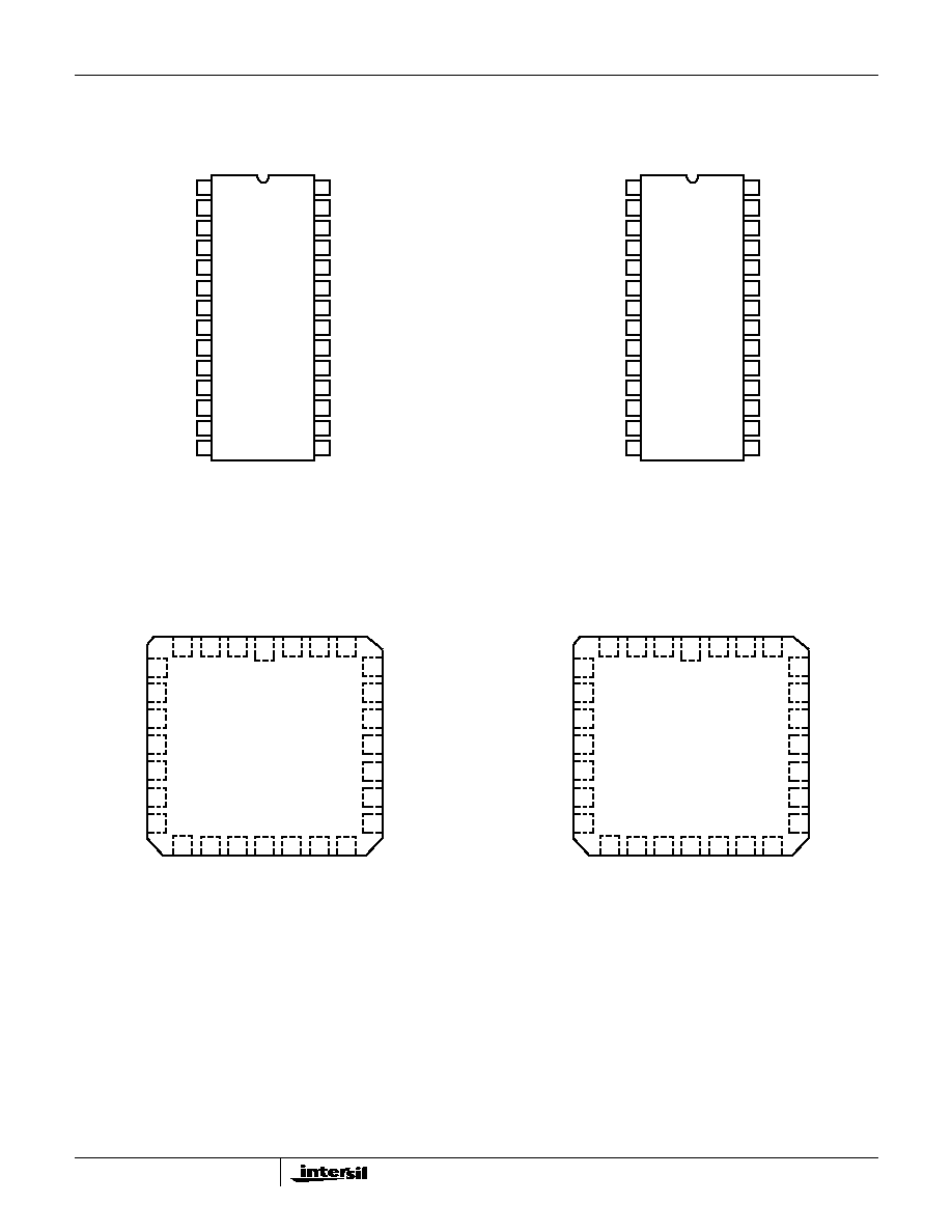
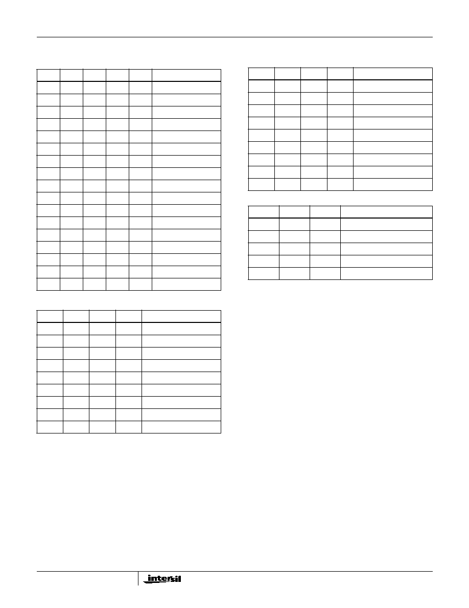
Ordering Information
PART NUMBER
TEMP.
RANGE (
o
C)
PACKAGE
PKG.
NO.
HI9P0506-9
-40 to 85
28 Ld SOIC
M28.3
HI3-0506-5
0 to 75
28 Ld PDIP
E28.6
HI4P0506-5
0 to 75
28 Ld PLCC
N28.45
HI1-0506-5
0 to 75
28 Ld CERDIP
F28.6
HI1-0506-4
-25 to 85
28 Ld CERDIP
F28.6
HI1-0506-2
-55 to 125
28 Ld CERDIP
F28.6
HI4P0507-5
0 to 75
28 Ld PLCC
N28.45
HI3-0507-5
0 to 75
28 Ld PDIP
E28.6
HI1-0507-2
-55 to 125
28 Ld CERDIP
F28.6
HI1-0508-5
0 to 75
16 Ld CERDIP
F16.3
HI3-0508-5
0 to 75
16 Ld PDIP
E16.3
HI1-0508-4
-25 to 85
16 Ld CERDIP
F16.3
HI1-0508-2
-55 to 125
16 Ld CERDIP
F16.3
HI4P0508-5
0 to 75
20 Ld PLCC
N20.35
HI9P0508-9
-40 to 85
16 Ld SOIC
M16.15
HI9P0508-5
0 to 75
16 Ld SOIC
M16.15
HI9P0509-5
0 to 75
16 Ld SOIC
M16.15
HI1-0509-4
-25 to 85
16 Ld CERDIP
F16.3
HI1-0509-5
0 to 75
16 Ld CERDIP
F16.3
HI3-0509-5
0 to 75
16 Ld PDIP
E16.3
HI4P0509-5
0 to 75
20 Ld PLCC
N20.35
HI1-0509-2
-55 to 125
16 Ld CERDIP
F16.3
Data Sheet
June 1999
CAUTION: These devices are sensitive to electrostatic discharge; follow proper IC Handling Procedures.
http://www.intersil.com or 407-727-9207
|
Copyright
©
Intersil Corporation 1999