1
Æ
CAUTION: These devices are sensitive to electrostatic discharge; follow proper IC Handling Procedures.
1-888-INTERSIL or 321-724-7143
|
Intersil (and design) is a registered trademark of Intersil Americas Inc.
Copyright © Intersil Americas Inc. 2003. All Rights Reserved
All other trademarks mentioned are the property of their respective owners.
8-Bit, 40/60/75/80 MSPS A/D Converter
The HI5714 is a high precision, monolithic, 8-bit, Analog-to-
Digital Converter fabricated in Intersil' advanced HBC10
BiCMOS process.
The HI5714 is optimized for a wide range of applications such as
ultrasound imaging, mass storage, instrumentation, and video
digitizing, where accuracy and low power consumption are
essential. The HI5714 is offered in 40 MSPS, 60 MSPS, and 75
MSPS sample rates.
The HI5714 delivers
±
0.4 LSB differential nonlinearity while
consuming only 325mW power (Typical) at 75 MSPS. The
digital inputs and outputs are TTL compatible, as well as
allowing for a low-level sine wave clock input.
Features
∑ Sampling Rate . . . . . . . . . . . . . . . . . . . 40/60/75/80 MSPS
∑ Low Power . . . . . . . . . . . . . . . . . . . . . . . . . . . . . .325mW
∑ 7.65 ENOB at 4.43MHz
∑ Overflow/Underflow Three-State TTL Output
∑ Operates with Low Level AC Clock
∑ Very Low Analog Input Capacitance
∑ No Buffer Amplifier Required
∑ No Sample and Hold Required
∑ TTL Compatible I/O
∑ Pin-Compatible to Philips TDA8714
Applications
∑ Video Digitizing
∑ QAM Demodulator
∑ Digital Cable Setup Box
∑ Tape Drive/Mass Storage
∑ Medical Ultrasound Imaging
∑ Communication Systems
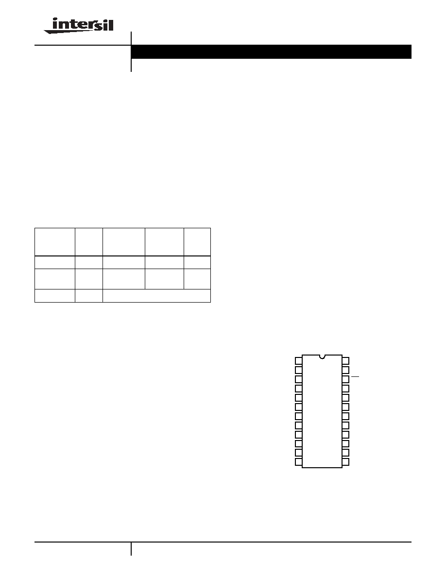
PinoutPinout
HI5714 (SOIC)
TOP VIEW
Ordering Information
PART
NUMBER
TEMP.
RANGE
(
o
C)
PACKAGE
SAMPLING
FREQUENCY
(MHz)
PKG.
NO.
HI5714/4CB
0 to 70 24 Ld SOIC
40
M24.3
HI5714/7CB-T 0 to 70 24 Ld SOIC
Tape & Reel
75
M24.3
HI5714EVAL
25
Evaluation Board
1
2
3
4
5
6
7
8
9
10
11
12
D1
D0
NC
V
RB
NC
AGND
V
CCA
V
IN
V
RT
NC
O/UF
D7
16
17
18
19
20
21
22
23
24
15
14
13
D2
OE
V
CCO2
OGND
V
CCO1
DGND
D4
D5
D6
D3
V
CCD
CLK
FN3973.5
HI5714
Data Sheet
April 2003
2
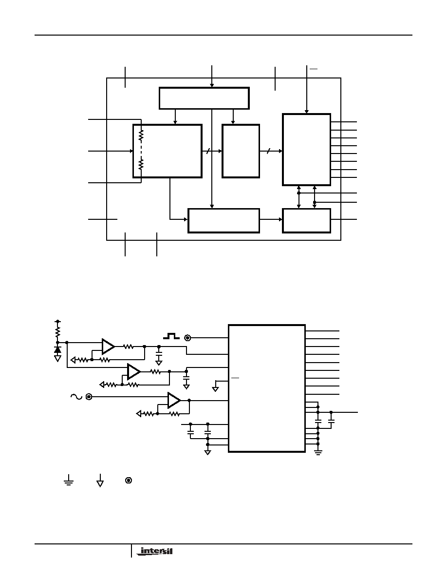
Functional Block Diagram
Typical Application Schematic
NOTES:
1. Pin 5 should be connected to AGND and pins 3 and 10 to DGND to reduce noise coupling into the device.
2. Analog and Digital supplies should be separated and decoupled to reduce digital noise coupling into the analog supply.
ANALOG TO DIGITAL
CONVERTER
LATCHES
TTL OUTPUTS
TTL OUTPUT
OVERFLOW/UNDERFLOW
LATCH
CLOCK DRIVER
V
CCA
CLK
V
CCD
OE
V
RT
V
RB
OGND
AGND
DGND
V
CCO1
V
CCO2
O/UF
V
IN
1
2
4
6
7
8
9
11
12
13
14
15
16
17
18
19
20
21
22
23
24
D7
D6
D5
D4
D3
D2
D1
D0
12
13
14
15
23
24
1
2
V
RB
HI5714
V
RT
CLK
DGND
NC
NC
AGND
V
CCA
V
CCD
D7
D6
D5
D4
D3
D2
D1
D0
as close to part as possible.
1nF and 0.1
µ
F CAPS are placed
CLOCK
V
IN
NC
V
IN
OGND
V
CCO
V
CCO
+5VA
O/UF
BNC
DGND
AGND
OE
11
19
21
18
20
3
17
10
16
9
4
8
7
5
6
22
3.6V
1.3V
+5VA
+5VD
1nF
0.1
µ
F
1nF
0.1
µ
F
0.1
0.1
-
+
-
+
-
+
HI5714
3
Absolute Maximum Ratings
T
A
= 25
o
C
Thermal Information
V
CCA
, V
CCD
, V
CCO
. . . . . . . . . . . . . . . . . . . . . . . . . . -0.3V to +6.0V
V
CCA
- V
CCD
. . . . . . . . . . . . . . . . . . . . . . . . . . . . . . . . . . . . . . ±0.3V
V
CCO
- V
CCD
. . . . . . . . . . . . . . . . . . . . . . . . . . . . . . . . . . . . . . ±0.3V
V
CCA
- V
CCO
. . . . . . . . . . . . . . . . . . . . . . . . . . . . . . . . . . . . . . ±0.3V
V
IN
, V
CLK
, V
RT
, V
RB
, OE . . . . . . . . . . . . . . . . . . . . . . -0.3V to +6.0V
I
OUT
, Digital Pins. . . . . . . . . . . . . . . . . . . . . . . . . . . . . . . . . . . 10mA
Input Current, All Pins . . . . . . . . . . . . . . . . . . . . . . . . . . . . . . . . 1mA
Digital I/O Pins . . . . . . . . . . . . . . . . . . . . . . . . . . . . . OGND to V
CCO
Operating Conditions
Temperature Range
HI5714/XCB . . . . . . . . . . . . . . . . . . . . . . . . . . . . . . . 0
o
C to 70
o
C
Thermal Resistance (Typical, Note 1)
JA
(
o
C/W)
SOIC Package . . . . . . . . . . . . . . . . . . . . . . . . . . . . .
75
Maximum Junction Temperature (Plastic Package) . . . . . . . .150
o
C
Maximum Storage Temperature Range . . . . . . . . . -65
o
C to 150
o
C
Maximum Lead Temperature (Soldering 10s) . . . . . . . . . . . . .300
o
C
(SOIC - Lead Tips Only)
CAUTION: Stresses above those listed in "Absolute Maximum Ratings" may cause permanent damage to the device. This is a stress only rating and operation of the
device at these or any other conditions above those indicated in the operational sections of this specification is not implied.
NOTE:
1.
JA
is measured with the component mounted on an evaluation PC board in free air.
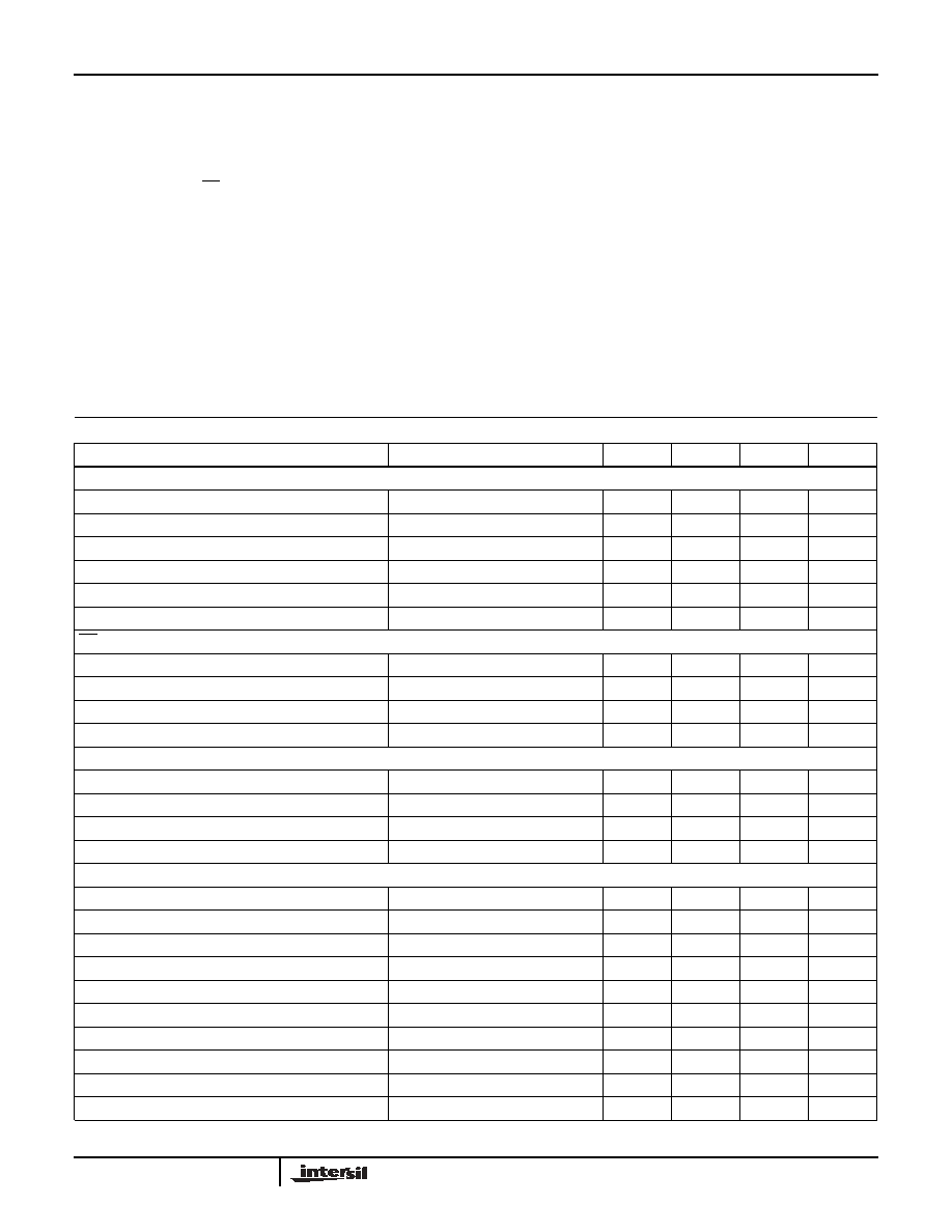
Electrical Specifications
V
CCA
= V
CCD
= V
CCO
= +5V; V
RB
= 1.3V; V
RT
= 3.6V; T
A
= 25
o
C, Unless Otherwise Specified
PARAMETER
TEST CONDITION
MIN
TYP
MAX
UNITS
CLOCK (Referenced to DGND) (Note 2)
Logic Input Voltage Low, V
IL
0
-
0.8
V
Logic Input Voltage High, V
IH
2.0
-
V
CCD
V
Logic Input Current Low, I
IL
V
CLK
= 0.4V
-400
-
-
µ
A
Logic Input Current High, I
IH
V
CLK
= 2.7V
-
-
300
µ
A
Input Impedance, Z
IN
f
CLK
= 75MHz (Note 9)
-
2
-
k
Input Capacitance, C
IN
f
CLK
= 75MHz (Note 9)
-
4.5
-
pF
OE (Referenced to DGND)
Logic Input Voltage Low, V
IL
0
-
0.8
V
Logic Input Voltage High, V
IH
2.0
-
V
CCD
V
Logic Input Current Low, I
IL
V
IL
= 0.4V
-400
-
-
µ
A
Logic Input Current High, I
IH
V
IH
= 2.7V
-
-
20
µ
A
V
IN
(Referenced to AGND)
Input Current Low, I
IL
V
IN
= 1.2V
-
0
-
µ
A
Input Current High, I
IH
V
IN
= 3.5V
-
100
180
µ
A
Input Impedance, Z
IN
f
IN
= 4.43MHz
-
10
-
k
Input Capacitance, C
IN
f
IN
= 4.43MHz
-
14
-
pF
REFERENCE INPUT
Bottom Reference Range, V
RB
1.2
1.3
1.6
V
Top Reference Range, V
RT
3.5
3.6
3.9
V
Reference Range, V
REF
(V
RT
- V
RB
)
1.9
2.3
2.7
V
Reference Current, I
REF
-
10
-
mA
Reference Ladder Resistance, R
LAD
-
240
-
R
LADTC
-
0.24
-
/
o
C
Bottom Offset Voltage, V
OB
(Note 5)
-
255
-
mV
V
OBTC
(Note 5)
-
136
-
µ
V/
o
C
Top Offset Voltage, V
OT
(Note 5)
-
-300
-
mV
V
OTTC
(Note 5)
-
480
-
µ
V/
o
C
HI5714

4
DIGITAL OUTPUTS (D0 to D7 and O/UF Referenced to OGND)
Logic Output Voltage Low, V
OL
I
O
= 1mA
0
-
0.4
V
Logic Output Voltage High, V
OH
I
O
= -0.4mA
2.7
-
V
CCO
V
Output Leakage Current, I
D
0.4V < V
OUT
< V
CCO
-20
-
+20
µ
A
SWITCHING CHARACTERISTICS (Notes 4, 5) See Figure 1
Sample Rate, f
CLK
HI5714/7
75
-
-
MHz
HI5714/4
40
-
-
MHz
Clock Pulse Width High, t
CPH
6
-
-
ns
Clock Pulse Width Low, t
CPL
6
-
-
ns
ANALOG SIGNAL PROCESSING (f
CLK
= 40MHz)
Differential Gain, DG
(Notes 6, 9)
-
1.0
-
%
Differential Phase, DP
(Notes 6, 9)
-
0.05
-
degree
HARMONICS (f
CLK
= 75MHz)
Second Harmonic, H2
f
IN
= 4.43MHz
-
-63
-
dB
Third Harmonic, H3
f
IN
= 4.43MHz
-
-65
-
dB
Total Harmonic Distortion, THD
f
IN
= 4.43MHz
-
-59
-
dB
Spurious Free Dynamic Range, SFDR
f
IN
= 4.43MHz
-
62
-
dB
Analog Input Bandwidth (-3dB)
-
18
-
MHz
TRANSFER FUNCTION
Differential Linearity Error, DNL
(Note 7)
-
±
0.4
-
LSB
Integral Linearity Error, INL
(Note 7)
-
±
0.75
-
LSB
EFFECTIVE NUMBER OF BITS
ENOB
HI5714/4 (f
CLK
= 40MHz)
f
IN
= 4.43MHz
-
7.65
-
Bits
f
IN
= 7.5MHz
-
7.5
-
Bits
HI5714/7 (f
CLK
= 75MHz)
f
IN
= 4.43MHz
-
7.4
-
Bits
f
IN
= 7.5MHz
-
7.15
-
Bits
f
IN
= 10MHz
-
6.8
-
Bits
Bit Error Rate, BER
(Note 8)
-
10
-11
-
Times/
Sample
TIMING (f
CLK
= 75MHz) See Figures 1, 2
Sampling Delay, t
SD
-
-
2
ns
Output Hold Time, t
HD
5
-
-
ns
Output Delay Time, t
D
HI5714/4/7
-
10
13
ns
Output Enable Delay, t
PZH
Enable to High
-
14.6
-
ns
Output Enable Delay, t
PZL
Enable to Low
-
17.8
-
ns
Output Disable Delay, t
PHZ
Disable from High
-
5.3
-
ns
Output Disable Delay, t
PLZ
Disable from Low
-
6.7
-
ns
Aperture Jitter, t
AJ
-
50
-
ps
Electrical Specifications
V
CCA
= V
CCD
= V
CCO
= +5V; V
RB
= 1.3V; V
RT
= 3.6V; T
A
= 25
o
C, Unless Otherwise Specified (Continued)
PARAMETER
TEST CONDITION
MIN
TYP
MAX
UNITS
HI5714

5
POWER SUPPLY CHARACTERISTICS
Analog Power Supply Range, V
CCA
4.75
5.0
5.25
V
Digital Power Supply Range, V
CCD
4.75
5.0
5.25
V
Output Power Supply Range, V
CCO
4.75
5.0
5.25
V
Total Supply Current
-
65
75
mA
Supply Current, I
CCA
-
30
-
mA
Supply Current, I
CCD
-
26
-
mA
Supply Current, I
CCO
-
9
-
mA
Power Dissipation
-
325
375
mW
NOTES:
2. Dissipation rating assumes device is mounted with all leads soldered to printed circuit board.
3. The supply voltages V
CCA
and V
CCD
may have any value between -0.3V and +6V as long as the difference V
CCA
- V
CCD
lies between
-0.3V and +0.3V.
4. In addition to a good layout of the digital and analog ground, it is recommended that the rise and fall times of the clock not be less than 1ns.
5. Analog input voltages producing code 00 up to and including FF. V
OB
(Bottom Offset Voltage) is the difference between the analog input which
produces data equal to 00 and the Bottom Reference Voltage (V
RB
). V
OBTC
(Bottom Offset Voltage Temperature Coefficient) is the variation
of V
OB
with temperature. V
OT
(Top Offset Voltage) is the difference between the Top Reference Voltage (V
RT
) and the analog input which
produces data output equal to FF. V
OTTC
(Top Offset Voltage Temperature Coefficient) is the variation of V
OT
with temperature.
6. Input is standard 5 step video test signal. A 12-bit R reconstruct DAC and VM700 are used for measurement.
7. Full scale sinewave, f
IN
= 4.43MHz.
8. f
CLK
= 75MHz, f
IN
= 4.43MHz, V
IN
=
±
8 LSB at code 128, 50% Clock duty cycle.
9. Parameter is guaranteed by design, not production tested.
Electrical Specifications
V
CCA
= V
CCD
= V
CCO
= +5V; V
RB
= 1.3V; V
RT
= 3.6V; T
A
= 25
o
C, Unless Otherwise Specified (Continued)
PARAMETER
TEST CONDITION
MIN
TYP
MAX
UNITS
HI5714