 | –≠–ª–µ–∫—Ç—Ä–æ–Ω–Ω—ã–π –∫–æ–º–ø–æ–Ω–µ–Ω—Ç: HI5760IA | –°–∫–∞—á–∞—Ç—å:  PDF PDF  ZIP ZIP |
1
HI5760
10-Bit, 125/60MSPS, High Speed D/A
Converter
The HI5760 is a 10-bit, 125MSPS, high speed, low power,
D/A converter which is implemented in an advanced CMOS
process. Operating from a single +3V to +5V supply, the
converter provides 20mA of full scale output current and
includes edge-triggered CMOS input data latches. Low glitch
energy and excellent frequency domain performance are
achieved using a segmented current source architecture. For
an equivalent performance dual version, see the HI5728.
This device complements the CommLinkTM HI5X60 family of
high speed converters offered by Intersil, which includes 8,
10, 12, and 14-bit devices.
Contact factory for availability.
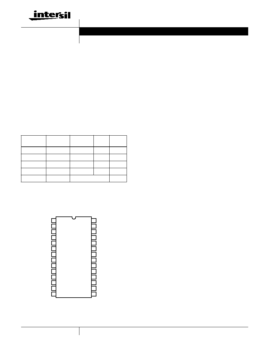
Pinout
HI5760 (SOIC, TSSOP)
TOP VIEW
Features
∑ Throughput Rate . . . . . . . . . . . . . . . . . . . . . . . .125MSPS
∑ Low Power . . . . . . . . . . . . . . . 165mW at 5V, 27mW at 3V
∑ Power Down Mode . . . . . . . . . . 23mW at 5V, 10mW at 3V
∑ Integral Linearity Error . . . . . . . . . . . . . . . . . . . . .
±
1 LSB
∑ Adjustable Full Scale Output Current . . . . . 2mA to 20mA
∑ SFDR to Nyquist at 5MHz Output . . . . . . . . . . . . . .68dBc
∑ Internal 1.2V Temperature Compensated Bandgap
Voltage Reference
∑ Single Power Supply from +5V to +3V
∑ CMOS Compatible Inputs
∑ Excellent Spurious Free Dynamic Range
Applications
∑ Cable Modems
∑ Set Top Boxes
∑ Wireless Communications
∑ Direct Digital Frequency Synthesis
∑ Signal Reconstruction
∑ Test Instrumentation
∑ High Resolution Imaging Systems
∑ Arbitrary Waveform Generators
Ordering Information
PART
NUMBER
TEMP.
RANGE (
o
C)
PACKAGE
PKG.
NO.
CLOCK
SPEED
HI5760BIB
-40 to 85
28 Ld SOIC
M28.3
125MHz
HI5760IA
-40 to 85
28 Ld TSSOP M28.173 125MHz
HI5760/6IB
-40 to 85
28 Ld SOIC
M28.3
60MHz
HI5760/6IA
-40 to 85
28 Ld TSSOP M28.173 60MHz
HI5760EVAL1
25
Evaluation Platform
125MHz
28
27
26
25
24
23
22
21
20
19
18
17
16
15
D9 (MSB)
D8
D7
D6
D5
D4
D3
D2
D1
D0 (LSB)
NC
NC
NC
NC
1
2
3
4
5
6
7
8
9
10
11
12
13
14
CLK
DCOM
NC
AV
DD
NC
IOUTB
COMP1
FSADJ
REFIO
REFLO
SLEEP
DV
DD
IOUTA
ACOM
Data Sheet
November 1999
File Number
4320.5
CAUTION: These devices are sensitive to electrostatic discharge; follow proper IC Handling Procedures.
1-888-INTERSIL or 321-724-7143
|
Copyright
©
Intersil Corporation 1999
CommLinkTM is a trademark of Intersil Corporation.
2
Typical Applications Circuit
Functional Block Diagram
D7 (3)
D6 (4)
D5 (5)
D4 (6)
D3 (7)
D2 (8)
D1 (9)
D0 (LSB) (10)
D7
D6
D5
D4
D3
D2
D1
D0
(11-14, 25)
DCOM (26)
CLK (28)
(19) COMP1
D/A OUT
(22) IOUTA
(21) IOUTB
50
(18) FSADJ
(16) REFLO
HI5760
D8
D9
D9 (MSB) (1)
D8 (2)
50
(20) ACOM
50
NC
(15) SLEEP
(17) REFIO
0.1
µ
F
2k
0.1
µ
F
(23) NC
D/A OUT
R
SET
(24) AV
DD
DV
DD
(27)
+5V OR +3V (V
DD
)
0.1
µ
F
10
µ
F
FERRITE
10
µ
H
0.1
µ
F
+
BEAD
10
µ
F
+
FERRITE
10
µ
H
BEAD
DCOM
ACOM
UPPER
VOLTAGE
REFERENCE
(LSB) D0
D1
D2
D3
D4
D5
D6
(MSB) D9
CLK
D7
D8
5-BIT
DECODER
REFIO
LATCH
AV
DD
ACOM
DV
DD
DCOM
LATCH
CASCODE
CURRENT
SOURCE
SWITCH
MATRIX
BIAS
GENERATION
INT/EXT
FSADJ
REFERENCE
INT/EXT
SELECT
REFLO
31
36
36
31 MSB
SEGMENTS
5 LSBs
+
COMP1
SLEEP
IOUTA
IOUTB
HI5760
3
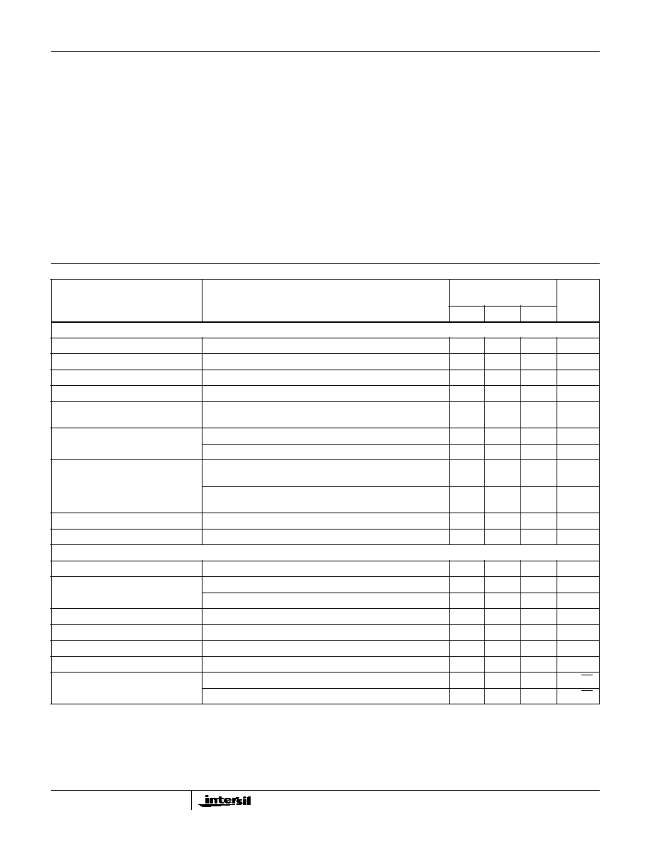
Absolute Maximum Ratings
Thermal Information
Digital Supply Voltage DV
DD
to DCOM . . . . . . . . . . . . . . . . . . +5.5V
Analog Supply Voltage AV
DD
to ACOM . . . . . . . . . . . . . . . . . . +5.5V
Grounds, ACOM TO DCOM. . . . . . . . . . . . . . . . . . . -0.3V To + 0.3V
Digital Input Voltages (D9-D0, CLK, SLEEP) . . . . . . DV
DD
+ 0.3V
Internal Reference Output Current
. . . . . . . . . . . . . . . . . . . . . . . ±
50
µ
A
Reference Input Voltage Range . . . . . . . . . . . . . . . . . . AV
DD
+ 0.3V
Analog Output Current (I
OUT
) . . . . . . . . . . . . . . . . . . . . . . . . . 24mA
Operating Conditions
Temperature Range . . . . . . . . . . . . . . . . . . . . . . . . . . -40
o
C to 85
o
C
Thermal Resistance (Typical, Note 1)
JA
(
o
C/W)
SOIC Package . . . . . . . . . . . . . . . . . . . . . . . . . . . . .
70
SSOP Package . . . . . . . . . . . . . . . . . . . . . . . . . . . .
117
Maximum Junction Temperature
HI5760 . . . . . . . . . . . . . . . . . . . . . . . . . . . . . . . . . . . . . . . . .150
o
C
Maximum Storage Temperature Range . . . . . . . . . . -65
o
C to 150
o
C
Maximum Lead Temperature (Soldering 10s) . . . . . . . . . . . . .300
o
C
(SOIC - Lead Tips Only)
CAUTION: Stresses above those listed in "Absolute Maximum Ratings" may cause permanent damage to the device. This is a stress only rating and operation of the
device at these or any other conditions above those indicated in the operational sections of this specification is not implied.
NOTE:
1.
JA
is measured with the component mounted on an evaluation PC board in free air.
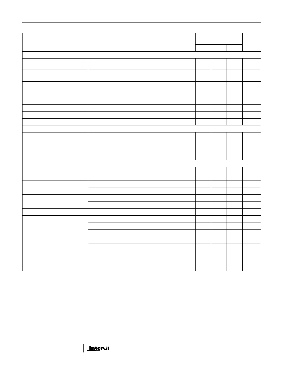
Electrical Specifications
AV
DD
= DV
DD
= +5V, V
REF
= Internal 1.2V, IOUTFS = 20mA, T
A
= 25
o
C for All Typical Values
PARAMETER
TEST CONDITIONS
HI5760
T
A
= -40
o
C TO 85
o
C
UNITS
MIN
TYP
MAX
SYSTEM PERFORMANCE
Resolution
10
-
-
Bits
Integral Linearity Error, INL
"Best Fit" Straight Line (Note 7)
-1
±
0.5
+1
LSB
Differential Linearity Error, DNL
(Note 7)
-0.5
±
0.25
+0.5
LSB
Offset Error, I
OS
(Note 7)
-0.025
+0.025
% FSR
Offset Drift Coefficient
(Note 7)
-
0.1
-
ppm
FSR/
o
C
Full Scale Gain Error, FSE
With External Reference (Notes 2, 7)
-10
±
2
+10
% FSR
With Internal Reference (Notes 2, 7)
-10
±
1
+10
% FSR
Full Scale Gain Drift
With External Reference (Note 7)
-
±
50
-
ppm
FSR/
o
C
With Internal Reference (Note 7)
-
±
100
-
ppm
FSR/
o
C
Full Scale Output Current, I
FS
2
-
20
mA
Output Voltage Compliance Range
(Note 3)
-0.3
-
1.25
V
DYNAMIC CHARACTERISTICS
Maximum Clock Rate, f
CLK
(Note 3)
125
-
-
MHz
Output Settling Time, (t
SETT
)
0.2% (
±
1 LSB, equivalent to 9 Bits) (Note 7)
-
20
-
ns
0.1% (
±
1/2 LSB, equivalent to 10 Bits) (Note 7)
-
35
-
ns
Singlet Glitch Area (Peak Glitch)
R
L
= 25
(Note 7)
-
5
-
pV∑s
Output Rise Time
Full Scale Step
-
1.0
-
ns
Output Fall Time
Full Scale Step
-
1.5
-
ns
Output Capacitance
-
10
-
pF
Output Noise
IOUTFS = 20mA
-
50
-
pA/
Hz
IOUTFS = 2mA
-
30
-
pA/
Hz
HI5760
4
AC CHARACTERISTICS - HI5760BIB, HI5760IA - 125MHz
Spurious Free Dynamic Range,
SFDR Within a Window
f
CLK
= 125MSPS, f
OUT
= 32.9MHz, 10MHz Span (Notes 4, 7)
-
75
-
dBc
f
CLK
= 100MSPS, f
OUT
= 5.04MHz, 4MHz Span (Notes 4, 7)
-
76
-
dBc
f
CLK
= 60MSPS, f
OUT
= 10.1MHz, 10MHz Span (Notes 4, 7)
-
75
-
dBc
f
CLK
= 50MSPS, f
OUT
= 5.02MHz, 2MHz Span (Notes 4, 7)
-
76
-
dBc
f
CLK
= 50MSPS, f
OUT
= 1.00MHz, 2MHz Span (Notes 4, 7)
-
78
-
dBc
Total Harmonic Distortion (THD) to
Nyquist
f
CLK
= 100MSPS, f
OUT
= 2.00MHz (Notes 4, 7)
-
71
-
dBc
f
CLK
= 50MSPS, f
OUT
= 2.00MHz (Notes 4, 7)
-
71
-
dBc
f
CLK
= 50MSPS, f
OUT
= 1.00MHz (Notes 4, 7)
-
76
-
dBc
Spurious Free Dynamic Range,
SFDR to Nyquist
f
CLK
= 125MSPS, f
OUT
= 32.9MHz, 62.5MHz Span (Notes 4, 7)
-
54
-
dBc
f
CLK
= 125MSPS, f
OUT
= 10.1MHz, 62.5MHz Span (Notes 4, 7)
-
64
-
dBc
f
CLK
= 100MSPS, f
OUT
= 40.4MHz, 50MHz Span (Notes 4, 7)
-
52
-
dBc
f
CLK
= 100MSPS, f
OUT
= 20.2MHz, 50MHz Span (Notes 4, 7)
-
60
-
dBc
f
CLK
= 100MSPS, f
OUT
= 5.04MHz, 50MHz Span (Notes 4, 7)
-
68
-
dBc
f
CLK
= 100MSPS, f
OUT
= 2.51MHz, 50MHz Span (Notes 4, 7)
-
74
-
dBc
f
CLK
= 60MSPS, f
OUT
= 10.1MHz, 30MHz Span (Notes 4, 7)
-
63
-
dBc
f
CLK
= 50MSPS, f
OUT
= 20.2MHz, 25MHz Span (Notes 4, 7)
-
55
-
dBc
f
CLK
= 50MSPS, f
OUT
= 5.02MHz, 25MHz Span (Notes 4, 7)
-
68
-
dBc
f
CLK
= 50MSPS, f
OUT
= 2.51MHz, 25MHz Span (Notes 4, 7)
-
73
-
dBc
f
CLK
= 50MSPS, f
OUT
= 1.00MHz, 25MHz Span (Notes 4, 7)
-
73
-
dBc
AC CHARACTERISTICS - HI5760/6IB, HI5760/6IA - 60MHz
Spurious Free Dynamic Range,
SFDR Within a Window
f
CLK
= 60MSPS, f
OUT
= 10.1MHz, 10MHz Span (Notes 4, 7)
-
75
-
dBc
f
CLK
= 50MSPS, f
OUT
= 5.02MHz, 2MHz Span (Notes 4, 7)
-
76
-
dBc
f
CLK
= 50MSPS, f
OUT
= 1.00MHz, 2MHz Span (Notes 4, 7)
-
78
-
dBc
Total Harmonic Distortion (THD) to
Nyquist
f
CLK
= 50MSPS, f
OUT
= 2.00MHz (Notes 4, 7)
-
71
-
dBc
f
CLK
= 50MSPS, f
OUT
= 1.00MHz (Notes 4, 7)
-
76
-
dBc
Spurious Free Dynamic Range,
SFDR to Nyquist
f
CLK
= 60MSPS, f
OUT
= 20.2MHz, 30MHz Span (Notes 4, 7)
-
56
-
dBc
f
CLK
= 60MSPS, f
OUT
= 10.1MHz, 30MHz Span (Notes 4, 7)
-
63
-
dBc
f
CLK
= 50MSPS, f
OUT
= 20.2MHz, 25MHz Span (Notes 4, 7)
-
55
-
dBc
f
CLK
= 50MSPS, f
OUT
= 5.02MHz, 25MHz Span (Notes 4, 7)
-
68
-
dBc
f
CLK
= 50MSPS, f
OUT
= 2.51MHz, 25MHz Span (Notes 4, 7)
-
73
-
dBc
f
CLK
= 50MSPS, f
OUT
= 1.00MHz, 25MHz Span (Notes 4, 7)
-
73
-
dBc
f
CLK
= 25MSPS, f
OUT
= 5.02MHz, 25MHz Span (Notes 4, 7)
-
71
-
dBc
VOLTAGE REFERENCE
Internal Reference Voltage, V
FSADJ
Pin 18 Voltage with Internal Reference
1.04
1.16
1.28
V
Internal Reference Voltage Drift
-
±
60
-
ppm
/
o
C
Internal Reference Output Current
Sink/Source Capability
-
0.1
-
µ
A
Reference Input Impedance
-
1
-
M
Reference Input Multiplying Bandwidth (Note 7)
-
1.4
-
MHz
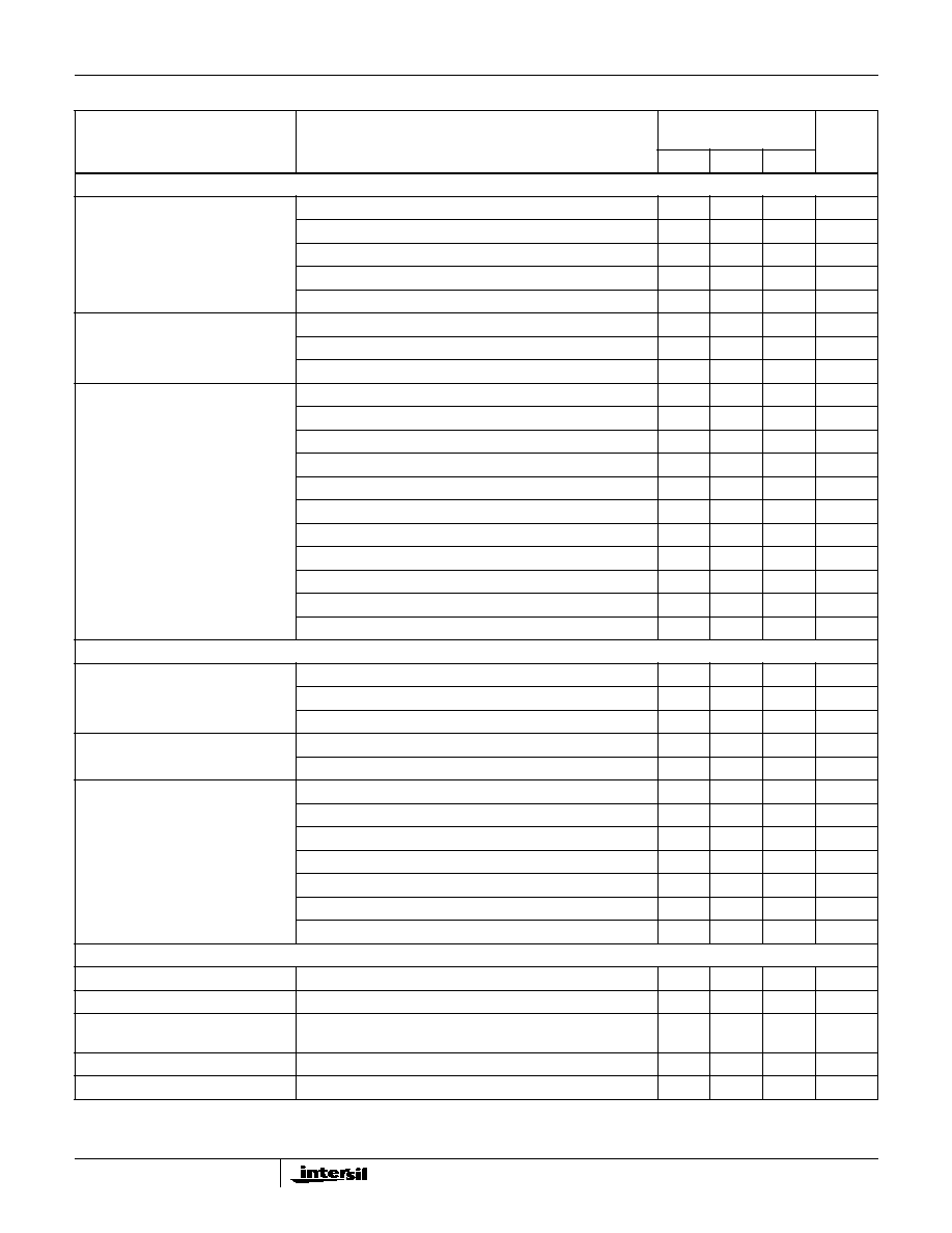
Electrical Specifications
AV
DD
= DV
DD
= +5V, V
REF
= Internal 1.2V, IOUTFS = 20mA, T
A
= 25
o
C for All Typical Values (Continued)
PARAMETER
TEST CONDITIONS
HI5760
T
A
= -40
o
C TO 85
o
C
UNITS
MIN
TYP
MAX
HI5760
5
DIGITAL INPUTS
D9-D0, CLK
Input Logic High Voltage with
5V Supply, V
IH
(Note 3)
3.5
5
-
V
Input Logic High Voltage with
3V Supply, V
IH
(Note 3)
2.1
3
-
V
Input Logic Low Voltage with
5V Supply, V
IL
(Note 3)
-
0
1.3
V
Input Logic Low Voltage with
3V Supply, V
IL
(Note 3)
-
0
0.9
V
Input Logic Current, I
IH
-10
-
+10
µ
A
Input Logic Current, I
IL
-10
-
+10
µ
A
Digital Input Capacitance, C
IN
-
5
-
pF
TIMING CHARACTERISTICS
Data Setup Time, t
SU
See Figure 41 (Note 3)
3
-
-
ns
Data Hold Time, t
HLD
See Figure 41 (Note 3)
3
-
-
ns
Propagation Delay Time, t
PD
See Figure 41
-
1
-
ns
CLK Pulse Width, t
PW1
, t
PW2
See Figure 41 (Note 3)
4
-
-
ns
POWER SUPPLY CHARACTERISTICS
AV
DD
Power Supply
(Note 8)
2.7
5.0
5.5
V
DV
DD
Power Supply
(Note 8)
2.7
5.0
5.5
V
Analog Supply Current (I
AVDD
)
(5V or 3V, IOUTFS = 20mA)
-
23
30
mA
(5V or 3V, IOUTFS = 2mA)
-
4
-
mA
Digital Supply Current (I
DVDD
)
(5V, IOUTFS = Don't Care) (Note 5)
-
3
5
mA
(3V, IOUTFS = Don't Care) (Note 5)
-
1.5
-
mA
Supply Current (I
AVDD
) Sleep Mode
(5V or 3V, IOUTFS = Don't Care)
-
1.6
3
mA
Power Dissipation
(5V, IOUTFS = 20mA) (Note 6)
-
165
-
mW
(5V, IOUTFS = 2mA) (Note 6)
-
70
-
mW
(5V, IOUTFS = 20mA) (Note 9)
-
150
-
mW
(3.3V, IOUTFS = 20mA) (Note 9)
-
75
-
mW
(3V, IOUTFS = 20mA) (Note 6)
-
85
-
mW
(3V, IOUTFS = 20mA) (Note 9)
-
67
-
mW
(3V, IOUTFS = 2mA) (Note 6)
-
27
-
mW
Power Supply Rejection
Single Supply (Note 7)
-0.2
-
+0.2
% FSR/V
NOTES:
2. Gain Error measured as the error in the ratio between the full scale output current and the current through R
SET
(typically 625
µ
A). Ideally the
ratio should be 31.969.
3. Parameter guaranteed by design or characterization and not production tested.
4. Spectral measurements made with differential coupled transformer.
5. Measured with the clock at 50MSPS and the output frequency at 1MHz.
6. Measured with the clock at 100MSPS and the output frequency at 40MHz.
7. See `Definition of Specifications'.
8. It is recommended that the output current be reduced to 12mA or less to maintain optimum performance for operation below 3V. DV
DD
and
AV
DD
do not have to be equal.
9. Measured with the clock at 60MSPS and the output frequency at 10MHz.
Electrical Specifications
AV
DD
= DV
DD
= +5V, V
REF
= Internal 1.2V, IOUTFS = 20mA, T
A
= 25
o
C for All Typical Values (Continued)
PARAMETER
TEST CONDITIONS
HI5760
T
A
= -40
o
C TO 85
o
C
UNITS
MIN
TYP
MAX
HI5760