
3-1
TM
CAUTION: These devices are sensitive to electrostatic discharge; follow proper IC Handling Procedures.
1-888-INTERSIL or 321-724-7143
|
Intersil and Design is a trademark of Intersil Corporation.
|
Copyright
©
Intersil Corporation 2000
HI5762
Dual 10-Bit, 60MSPS A/D Converter with
Internal Voltage Reference
The HI5762 is a monolithic, dual 10-bit, 60MSPS analog-to-
digital converter fabricated in an advanced CMOS process.
It is designed for high speed applications where integration,
bandwidth and accuracy are essential. Built by combining
two cores of the HI5767 single channel 10-bit 60MSPS
analog-to-digital converter, the HI5762 reaches a new level
of multi-channel integration. The fully pipeline architecture
and an innovative input stage enable the HI5762 to accept a
variety of input configurations, single-ended or fully
differential. Only one external clock is necessary to drive
both converters and an internal band-gap voltage reference
is provided. This allows the system designer to realize an
increased level of system integration resulting in decreased
cost and power dissipation.
The HI5762 has excellent dynamic performance while
consuming only 650mW of power at 60MSPS. The A/D only
requires a single +5V power supply and encode clock. Data
output latches are provided which present valid data to the
output bus with a latency of 6 clock cycles.
For those customers needing dual channel 8-bit resolution,
please refer to the HI5662. For single channel 10-bit
applications, please refer to the HI5767.
Features
∑ Sampling Rate . . . . . . . . . . . . . . . . . . . . . . . . . . .60MSPS
∑ 8.8 Bits at f
IN
= 10MHz
∑ Low Power at 60MSPS. . . . . . . . . . . . . . . . . . . . . 650mW
∑ Wide Full Power Input Bandwidth. . . . . . . . . . . . . 250MHz
∑ Excellent Channel-to-Channel Isolation . . . . . . . . . >75dB
∑ On-Chip Sample and Hold Amplifiers
∑ Internal Band-Gap Voltage Reference . . . . . . . . . . . . 2.5V
∑ Fully Differential or Single-Ended Analog Inputs
∑ Single Supply Voltage Operation . . . . . . . . . . . . . . . . +5V
∑ TTL/CMOS Compatible Sampling Clock Input
∑ CMOS Compatible Digital Outputs . . . . . . . . . . . . 3.0/5.0V
∑ Offset Binary Digital Data Output Format
∑ Dual 10-Bit A/D Converters on a Monolithic Chip
Applications
∑ Wireless Local Loop
∑ PSK and QAM I&Q Demodulators
∑ Medical Imaging
∑ High Speed Data Acquisition
Pinout
HI5762 (MQFP)
TOP VIEW
Ordering Information
PART
NUMBER
TEMP.
RANGE (
o
C)
PACKAGE
PKG. NO.
HI5762/6IN
-40 to 85
44 Ld MQFP
Q44.10x10
HI5762EVAL2
25
Evaluation Platform
1
2
3
4
5
6
7
8
9
10
11
12 13 14 15 16 17
28
27
26
25
24
23
22
21
20
19
18
39 38 37 36 35 34
33
32
31
30
29
44 43 42 41 40
A
GND
AV
CC2
ID8
ID7
ID6
ID5
DV
CC3
D
GND
ID4
ID3
ID9
A
GND
AV
CC2
QD8
QD7
QD6
QD5
DV
CC3
D
GND
QD4
QD3
QD9
ID2
ID1
ID0
D
GND
DV
CC1
CLK
DV
CC2
D
GND
QD0
QD1
QD2
IV
DC
I
IN-
I
IN+
A
GND
V
RIN
NC
V
R
OUT
AV
CC1
Q
IN+
Q
IN-
QV
DC
Data Sheet
February 1999
File Number
4318.2

3-2
Functional Block Diagram
DV
CC3
+
-
STAGE 1
STAGE 8
CLOCK
BIAS
I/QV
DC
I/Q
IN
-
I/Q
IN
+
I/QD0 (LSB)
I/QD1
I/QD2
I/QD3
I/QD4
I/QD5
I/QD6
I/QD7
I/QD8
I/QD9 (MSB)
CLK
AV
CC1,2
AGND
DV
CC1,2
DGND
STAGE 9
X2
S/H
2-BIT
FLASH
2-BIT
DAC
+
-
X2
2-BIT
FLASH
2-BIT
DAC
2-BIT
FLASH
DIGITAL DELAY
AND
DIGITAL ERROR
CORRECTION
REFERENCE
V
REFOUT
V
REFIN
I or Q CHANNEL
HI5762
3-3
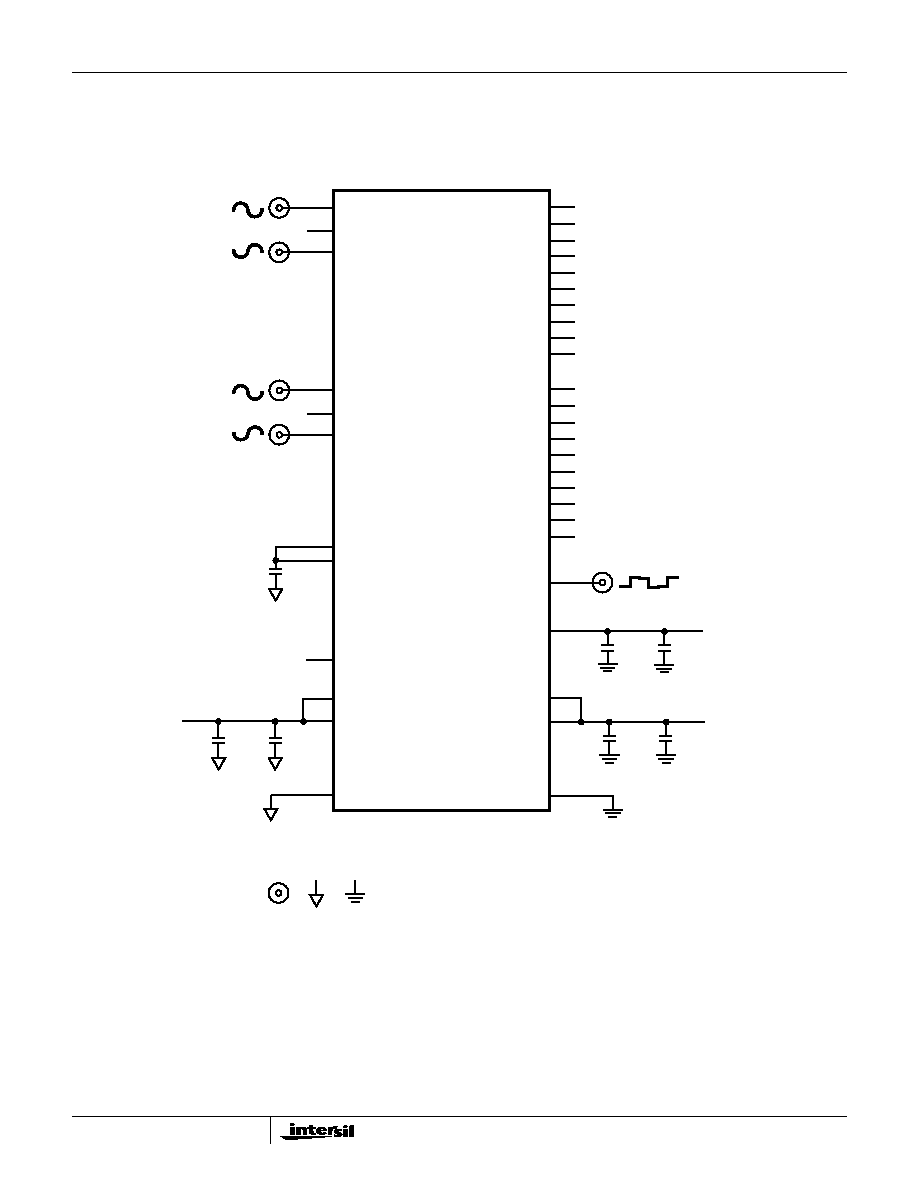
Typical Application Schematic
ARE PLACED AS CLOSE
10
µ
F AND 0.1
µ
F CAPS
QD9
QD8
QD7
QD6
QD5
QD4
QD3
QD2
QD1
QD0
BNC
CLOCK
10
µ
F
0.1
µ
F
10
µ
F
+
+
DGND
AGND
(38) V
ROUT
(40) V
RIN
CLK (17)
DGND (9,15,19,25)
(1,33,41) AGND
(LSB) QD0 (20)
QD1 (21)
QD2 (22)
QD3 (23)
QD4 (24)
QD5 (27)
QD6 (28)
QD7 (29)
QD8 (30)
(MSB) QD9 (31)
(2,32) AV
CC2
(37) AV
CC1
DV
CC1
(16)
TO PART AS POSSIBLE
0.1
µ
F
+5V
+5V
0.1
µ
F
ID9
ID8
ID7
ID6
ID5
ID4
ID3
ID2
ID1
ID0
(LSB) ID0 (14)
ID1 (13)
ID2 (12)
ID3 (11)
ID4 (10)
ID5 (7)
ID6 (6)
ID7 (5)
ID8 (4)
(MSB) ID9 (3)
I
IN
+
I
IN
-
(43) I
IN
-
(42) I
IN
+
(44) IV
DC
0.1
µ
F
10
µ
F
+
DV
CC3
(8,26)
+5V or +3V
DV
CC2
(18)
(39) NC
Q
IN
+
Q
IN
-
(35) Q
IN
-
(36) Q
IN
+
(34) QV
DC
HI5762
HI5762

3-4
Pin Descriptions
PIN NO.
NAME
DESCRIPTION
1
A
GND
Analog Ground
2
AV
CC2
Analog Supply (+5.0V)
3
ID9
I-Channel, Data Bit 9 Output (MSB)
4
ID8
I-Channel, Data Bit 8 Output
5
ID7
I-Channel, Data Bit 7 Output
6
ID6
I-Channel Data Bit 6 Output
7
ID5
I-Channel, Data Bit 5 Output
8
DV
CC3
Digital Output Supply
(+3.0V or +5.0V)
9
D
GND
Digital Ground
10
ID4
I-Channel, Data Bit 4 Output
11
ID3
I-Channel, Data Bit 3 Output
12
ID2
I-Channel, Data Bit 2 Output
13
ID1
I-Channel, Data Bit 1 Output
14
ID0
I-Channel, Data Bit 0 Output (LSB)
15
D
GND
Digital Ground
16
DV
CC1
Digital Supply (+5.0V)
17
CLK
Sample Clock Input
18
DV
CC2
Digital Supply (+5.0V)
19
D
GND
Digital Ground
20
QD0
Q-Channel, Data Bit 0 Output (LSB)
21
QD1
Q-Channel, Data Bit 1 Output
22
QD2
Q-Channel, Data Bit 2 Output
23
QD3
Q-Channel, Data Bit 3 Output
24
QD4
Q-Channel, Data Bit 4 Output
25
DGND
Digital Ground
26
DV
CC3
Digital Output Supply
(+3.0V or +5.0V)
27
QD5
Q-Channel, Data Bit 5 Output
28
QD6
Q-Channel, Data Bit 6 Output
29
QD7
Q-Channel, Data Bit 7 Output
30
QD8
Q-Channel, Data Bit 8 Output
31
QD9
Q-Channel, Data Bit 9 Output
(MSB)
32
AV
CC2
Analog Supply (+5.0V)
33
A
GND
Analog Ground
34
QV
DC
Q-Channel DC Bias Voltage Output
35
Q
IN-
Q-Channel Negative Analog Input
36
Q
IN+
Q-Channel Positive Analog Input
37
AV
CC1
Analog Supply (+5.0V)
38
V
ROUT
+2.5V Reference Voltage Output
39
NC
No Connect
40
V
RIN
+2.5V Reference Voltage Input
41
A
GND
Analog Ground
42
I
IN+
I-Channel Positive Analog Input
43
I
IN-
I-Channel Negative Analog Input
44
IV
DC
I-Channel DC Bias Voltage Output
PIN NO.
NAME
DESCRIPTION
HI5762

3-5
Absolute Maximum Ratings
T
A
= 25
o
C
Thermal Information
Supply Voltage, AV
CC
or DV
CC
to AGND or DGND . . . . . . . . . . .6V
DGND to AGND . . . . . . . . . . . . . . . . . . . . . . . . . . . . . . . . . . . . . 0.3V
Digital I/O Pins . . . . . . . . . . . . . . . . . . . . . . . . . . . . . DGND to DV
CC
Analog I/O Pins . . . . . . . . . . . . . . . . . . . . . . . . . . . . AGND to AV
CC
Operating Conditions
Temperature Range
HI5762/6IN . . . . . . . . . . . . . . . . . . . . . . . . . . . . . . . -40
o
C to 85
o
C
Thermal Resistance (Typical, Note 1)
JA
(
o
C/W)
HI5762/6IN . . . . . . . . . . . . . . . . . . . . . . . . . . . . . . . .
75
Maximum Junction Temperature . . . . . . . . . . . . . . . . . . . . . . .150
o
C
Maximum Storage Temperature Range . . . . . . . . . . -65
o
C to 150
o
C
Maximum Lead Temperature (Soldering 10s) . . . . . . . . . . . . .300
o
C
(Lead Tips Only)
CAUTION: Stresses above those listed in "Absolute Maximum Ratings" may cause permanent damage to the device. This is a stress only rating and operation of the
device at these or any other conditions above those indicated in the operational sections of this specification is not implied.
NOTE:
1.
JA
is measured with the component mounted on an evaluation PC board in free air.
Electrical Specifications
AV
CC1,2
= DV
CC1,2
= +5.0V, DV
CC3
= +3.0V; V
RIN
= 2.50V; f
S
= 60MSPS at 50% Duty Cycle;
C
L
= 10pF; T
A
= 25
o
C; Differential Analog Input; Unless Otherwise Specified
PARAMETER
TEST CONDITIONS
MIN
TYP
MAX
UNITS
ACCURACY
Resolution
10
-
-
Bits
Integral Linearity Error, INL
f
IN
= 10MHz
-
2
-
LSB
Differential Linearity Error, DNL
(Guaranteed No Missing Codes)
f
IN
= 10MHz
-
±
0.4
±
1.0
LSB
Offset Error, V
OS
f
IN
= DC
-40
-
+40
LSB
Full Scale Error, FSE
f
IN
= DC
-
4
-
LSB
DYNAMIC CHARACTERISTICS
Minimum Conversion Rate
No Missing Codes
-
1
-
MSPS
Maximum Conversion Rate
No Missing Codes
60
-
-
MSPS
Effective Number of Bits, ENOB
f
IN
= 10MHz
8.4
8.8
-
Bits
Signal to Noise and Distortion Ratio, SINAD
f
IN
= 10MHz
-
54.7
-
dB
Signal to Noise Ratio, SNR
f
IN
= 10MHz
-
54.7
-
dB
Total Harmonic Distortion, THD
f
IN
= 10MHz
-
-68
-
dBc
2nd Harmonic Distortion
f
IN
= 10MHz
-
-70
-
dBc
3rd Harmonic Distortion
f
IN
= 10MHz
-
-73
-
dBc
Spurious Free Dynamic Range, SFDR
f
IN
= 10MHz
-
70
-
dBc
Intermodulation Distortion, IMD
f
1
= 1MHz, f
2
= 1.02MHz
-
64
-
dBc
I/Q Channel Crosstalk
-
-75
-
dBc
I/Q Channel Offset Match
-
10
-
LSB
I/Q Channel Full Scale Error Match
-
10
-
LSB
Transient Response
(Note 2)
-
1
-
Cycle
Over-Voltage Recovery
0.2V Overdrive (Note 2)
-
1
-
Cycle
ANALOG INPUT
Maximum Peak-to-Peak Differential Analog Input
Range (V
IN
+ - V
IN
-)
-
±
0.5
-
V
Maximum Peak-to-Peak Single-Ended
Analog Input Range
-
1.0
-
V
RMS Signal
RMS Noise + Distortion
--------------------------------------------------------------
=
RMS Signal
RMS Noise
-------------------------------
=
HI5762