 | –≠–ª–µ–∫—Ç—Ä–æ–Ω–Ω—ã–π –∫–æ–º–ø–æ–Ω–µ–Ω—Ç: HIP4011IS | –°–∫–∞—á–∞—Ç—å:  PDF PDF  ZIP ZIP |
6-11
CAUTION: These devices are sensitive to electrostatic discharge; follow proper IC Handling Procedures.
407-727-9207
|
Copyright
©
Intersil Corporation 1999
[ /Title (HIP4011)
/Subject (Three Phase Brushless DC Motor Controller)
/Author ()
/Keywords ()
/Creator ()
/DOCINFO pdfmark
[ /PageMode /UseOutlines
/DOCVIEW pdfmark
HIP4011
Three Phase Brushless DC Motor Controller
Description
The HIP4011 motor driver is intended for three phase Brush-
less motor control at continuous output currents up to 3A. It
accepts inputs from buffered Hall effect sensors and drives
three motor windings, regulating the current through an
external current sensing resistor, according to an analog
control input. Output "freewheeling" diodes are built in and
output dv/dt is limited to decrease the generated EMI.
Thermal and current limiting are used to protect the device
from locked rotor conditions. A brake control input forces all
outputs to ground simultaneously to provide dynamic
braking, and an internal voltage sensor does the same when
the supply drops below a predetermined switch point. Power
down braking energy is stored in an external capacitor.
Ordering Information
PART
NUMBER
TEMPERATURE
RANGE
PACKAGE
HIP4011IS
-40
o
C to +85
o
C
15 Pin Plastic SIP
Surface Mount
Features
∑ 3A DC, 5A Peak Output Current
∑ 16V Max. Rated Supply Voltage
∑ Built-in "Free-Wheeling" Diodes
∑ Output dv/dt Limited to Reduce EMI
∑ External Dynamic Brake Control Switch With
Undervoltage Sense
∑ Thermal and Current Limiting Protects Against
Locked Rotor Conditions
∑ Provides Analog Current Sense and Reference Inputs
∑ Decode Logic with Illegal Code Rejection
Applications
∑ Drive Spindle Motor Controller
∑ 3 Phase Brushless DC Motor Controller
∑ Brushless DC Motor Driver for 12V Battery Powered
Appliances
∑ Phased Driver for 12V DC Applications
∑ Logic Controlled Driver for Solenoids, Relays and
Lamps
File Number
2939.3
April 1994
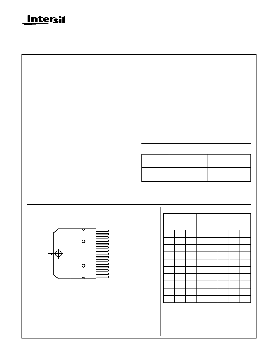
Pinout
HIP4011 (SIP)
TOP VIEW
PGND PIN
(TAB) MUST BE
ELECTRICALLY
CONNECTED
15
14
13
12
11
10
9
8
7
6
5
4
3
2
1
SGND = SIGNAL GROUND
SENA = SENSE INPUT A
SENB = SENSE INPUT B
SENC = SENSE INPUT C
PV+
= POWER V+
FBRK = FORCED BRAKE
OUTC = OUTPUT C
ISEN
= ISENSE
OUTB = OUTPUT B
PV+
= POWER V+
BCAP = BRAKING CAPACITOR
OUTA = OUTPUT A
ISEN
= ISENSE
SV+
= SIGNAL V+
SPD
= SPEED CONTROL
* Undervoltage and Force Brake logic truth table
entries are identical.
"X" = Don't Care
OUTPUT TRUTH TABLE
SENSOR
INPUTS
FORCE
BRAKE
INPUT*
OUTPUTS
A
B
C
FBRK
A
B
C
0
0
0
0
OFF
OFF
OFF
1
0
0
0
1
OFF
0
0
1
0
0
0
1
OFF
1
1
0
0
OFF
1
0
0
0
1
0
OFF
0
1
1
0
1
0
1
0
OFF
0
1
1
0
0
OFF
1
1
1
1
0
OFF
OFF
OFF
X
X
X
1
0
0
0
6-12
Specifications HIP4011
Absolute Maximum Ratings
Thermal Information
Supply Voltage, SV+ or PV+. . . . . . . . . . . . . . . . . . . . . . -1V to +16V
Referred to SGND or PGND (Note 1)
Output Current, Continuous . . . . . . . . . . . . . . . . . . . . . . . . . . . . . 3A
Output Current, Peak (Note 2) . . . . . . . . . . . . . . . . . . . . . . . . . . . 5A
Substrate (PGND) Current . . . . . . . . . . . . . . . . . . . . . . . . . . . . . . 1A
Logic Input Current . . . . . . . . . . . . . . . . . . . . . . . . . -20mA to +20mA
(Clamped to SV+ and SGND)
Thermal Resistance
JA
JC
15 Lead SIP Power Package. . . . . . . . . .
45
o
C/W
3
o
C/W
Power Dissipation (Note 3) . . . . . . . . . . . . . . . . . . . . . . . . . . . . 25W
Junction Temperature Range, Operating . . . . . . . . . . . . . . . +150
o
C
Storage Temperature Range. . . . . . . . . . . . . . . . . . -55
o
C to +150
o
C
Power Dissipation
Up to +125
o
C without heat sink . . . . . . . . . . . . . . . . . . . . . 0.56W
Above +125
o
C without Heat Sink . . Derate Linearly at 22mW/
o
C
Up to +125
o
C with Infinite Heat Sink . . . . . . . . . . . . . . . . . 8.33W
Above +125
o
C with Infinite Heat Sink . . . . . . . . . . . . . . . . . . . . . .
. . . . . . . . . . . . . . . . . . . . . . . . . . . . .Derate Linearly at 333mW/
o
C
Lead Temperature (During Soldering)
At a Distance 1/16 inch
±
1/32 inch (1.59mm
±
0.79mm)
from Case for 10s Max. . . . . . . . . . . . . . . . . . . . . . . . . . +265
o
C
NOTES:
1. PV+ and SV+ are to be tied together, as are PGND and SGND.
2. Operating above the continuous current rating causes a decrease in operating life.
3. Derate power dissipation above case temperature of +75
o
C at 0.33 Watts/
o
C.
CAUTION: Stresses above those listed in "Absolute Maximum Ratings" may cause permanent damage to the device. This is a stress only rating and operation
of the device at these or any other conditions above those indicated in the operational sections of this specification is not implied.
Electrical Specifications
T
A
= +25
o
C and SV+ = PV+ = 10.4V to 13.2V, Unless Otherwise Specified
PARAMETERS
TEST CONDITION
MIN
TYP
MAX
UNITS
SUPPLY (SV+) CURRENT
No Drive
Outputs Off
-
-
10
mA
With Drive
Outputs On
-
-
15
mA
LOGIC INPUT CURRENT
Sensor Inputs
SENA, SENB & SENC = 0V to 3V
-0.5
-
-1.5
mA
Brake Input
FBRK = 0.8V to 2.4V
50
-
150
µ
A
LOGIC INPUT THRESHOLDS
Sensor Inputs
Logic "0" Input Voltage
-
-
1.8
V
Sensor Inputs
Logic "1" Input Voltage
3
-
-
V
Brake Input
Logic "0" Input Voltage
-
-
0.8
V
Brake Input
Logic "1" Input Voltage
2.4
-
-
V
AMPLIFIER INPUT (SPD)
Bias Current
-
-
700
nA
Offset Voltage
-
-
3
mV
Input Range (Linear)
0
-
1
V
Input Impedance
1
-
-
M
System Bandwidth
(Note 1)
-
35
-
kHz
Current Limit
Rsense = 0.20
-
5
-
A
THERMAL LIMIT
Threshold
-
155
-
o
C
Hysteresis
-
40
-
o
C
OUTPUT DRIVERS
On Saturation (See Note 5)
I
OUT
= 3A, V
PMOS
+ V
NMOS
-
-
2.2
V
On Saturation (See Note 5)
I
OUT
= 0.6A, V
PMOS
+ V
NMOS
-
-
0.44
V
Off Leakage
PV+ > V
OUT
> PGND or I
SEN
-
-
1
mA
Slew Rate
(See Note 2)
-
0.5
-
V/
µ
S

6-13
HIP4011
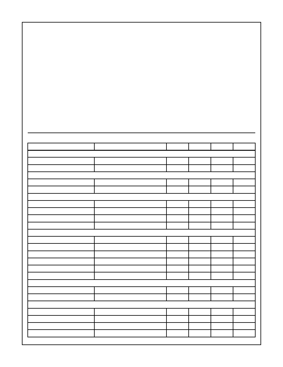
Functional Block Diagram
FREEWHEEL DIODES
Forward Drop
I
OUT
= 1A
-
-
1.5
V
INTERNAL BRAKE DRIVER
Undervoltage Trip Point, PV+
(See Note 3)
2.7
-
3.3
V
Hysteresis
(See Note 4)
40
-
60
%
On Saturation
Each N
MOS
, I
OUT
= 3A
-
-
0.4
V
BRAKE CAPACITOR (BCAP)
Discharge Leakage
SV+ = PV+ = 3V to 12V, BCAP = 10V
-
-
5
µ
A
NOTES:
1. The system bandwidth is fixed by an internal RC network around the amplifier.
2. Internal limiting of turn on and turn off drive is used to limit output dv/dt.
3. The braking action starts at the given trip point with a falling supply voltage.
4. Hysteresis causes the brake to be removed at a higher trip point with a rising supply voltage.
5. This value includes the combined voltage drops of one upper plus one lower switch at the indicated current.
Electrical Specifications
T
A
= +25
o
C and SV+ = PV+ = 10.4V to 13.2V, Unless Otherwise Specified
(Continued)
PARAMETERS
TEST CONDITION
MIN
TYP
MAX
UNITS
SENA
1
HALL
SENSOR
A
SENB
2
HALL
SENSOR
B
SENC
3
HALL
SENSOR
C
FBRK
6
FORCE
BRAKE
13
SIGNAL
V+
1mA
V+
V+
1mA
1mA
BREAK
BEFORE
MAKE
THERMAL
SENSING
DECODE
LOGIC
WITH
ILLEGAL
CODE
REJECTION
100
µ
A
V+
VBS (BRAKE
(SENSE REF)
V
CL
CURRENT
SENSE
RESISTOR
(CURRENT LIMITING
REF)
CURRENT
LIMITING
+
-
V+
BCAP
10
4 PV+
OUTA
11
OUTB
8
9 PV+
BRAKE
CAP.
POWER V+
MOTOR
A
MOTOR
C
MOTOR
B
OUTC
5
ISEN
12
ISEN
7
IREF
14
SIGNAL
GND
15
SGND
PGND
TAB
SUBSTRATE
GND
39K
R
1
39K
C
1
100pF
38.5K
1K 1K
R
2

6-14
All Intersil semiconductor products are manufactured, assembled and tested under ISO9000 quality systems certification.
Intersil products are sold by description only. Intersil Corporation reserves the right to make changes in circuit design and/or specifications at any time without
notice. Accordingly, the reader is cautioned to verify that data sheets are current before placing orders. Information furnished by Intersil is believed to be accurate
and reliable. However, no responsibility is assumed by Intersil or its subsidiaries for its use; nor for any infringements of patents or other rights of third parties which
may result from its use. No license is granted by implication or otherwise under any patent or patent rights of Intersil or its subsidiaries.
For information regarding Intersil Corporation and its products, see web site http://www.intersil.com
Sales Office Headquarters
NORTH AMERICA
Intersil Corporation
P. O. Box 883, Mail Stop 53-204
Melbourne, FL 32902
TEL: (407) 727-9207
FAX: (407) 724-7240
EUROPE
Intersil SA
Mercure Center
100, Rue de la Fusee
1130 Brussels, Belgium
TEL: (32) 2.724.2111
FAX: (32) 2.724.22.05
ASIA
Intersil (Taiwan) Ltd.
Taiwan Limited
7F-6, No. 101 Fu Hsing North Road
Taipei, Taiwan
Republic of China
TEL: (886) 2 2716 9310
FAX: (886) 2 2715 3029
HIP4011
File Number