188
TM
March 1997
HM-65162/883
2K x 8 Asynchronous
CMOS Static RAM
Features
∑ This Circuit is Processed in Accordance to MIL-STD-
883 and is Fully Conformant Under the Provisions of
Paragraph 1.2.1.
∑ Fast Access Time . . . . . . . . . . . . . . . . . . . 70/90ns Max
∑ Low Standby Current. . . . . . . . . . . . . . . . . . . .50
µ
A Max
∑ Low Operating Current . . . . . . . . . . . . . . . . . 70mA Max
∑ Data Retention at 2.0V . . . . . . . . . . . . . . . . . . .20
µ
A Max
∑ TTL Compatible Inputs and Outputs
∑ JEDEC Approved Pinout (2716, 6116 Type)
∑ No Clocks or Strobes Required
∑ Wide Temperature Range . . . . . . . . . . -55
o
C to +125
o
C
∑ Equal Cycle and Access Time
∑ Single 5V Supply
∑ Gated Inputs
- No Pull-Up or Pull-Down Resistors Required
Description
The HM-65162/883 is a CMOS 2048 x 8 Static Random
Access Memory manufactured using the Intersil Advanced
SAJI V process. The device utilizes asynchronous circuit
design for fast cycle time and ease of use. The pinout is the
JEDEC 24 pin DIP, and 32 pad 8-bit wide standard which
allows easy memory board layouts flexible to accommodate
a variety of industry standard PROMs, RAMs, ROMs and
EPROMs. The HM-65162/883 is ideally suited for use in
microprocessor based systems with its 8-bit word length
organization. The convenient output enable also simplifies
the bus interface by allowing the data outputs to be con-
trolled independent of the chip enable. Gated inputs lower
operating current and also eliminate the need for pull-up or
pull-down resistors.
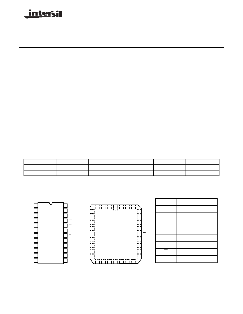
Pinouts
Ordering Information
70ns/20
µ
A
90ns/40
µ
A
90ns/300
µ
A
TEMP. RANGE
PACKAGE
PKG. NO.
HM1-65162B/883
HM1-65162/883
HM1-65162C/883
-55
o
C to 125
o
C
CERDIP
F24.6
HM4-65162B/883
HM4-65162/883
-
-55
o
C to 125
o
C
CLCC
J32.A
HM-65162/883 (CERDIP)
TOP VIEW
HM-65162/883 (CLCC)
TOP VIEW
1
2
3
4
5
6
7
8
9
10
11
12
16
17
18
19
20
21
22
23
24
15
14
13
VCC
A9
W
G
A10
DQ7
DQ5
DQ4
DQ3
A8
E
DQ6
A7
A6
A5
A4
A3
A2
A1
A0
DQ0
DQ1
DQ2
GND
5
6
7
8
11
10
9
13
12
27
28
29
26
25
24
23
22
21
3
2
1
4
32 31 30
16 17 18 19 20
14 15
A6
A5
A4
A3
A2
A1
A0
NC
DQ0
DQ
1
DQ
2
GN
D
NC
DQ
3
DQ
4
DQ
5
VC
C
NC
NC
A7
NC
NC
NC
A8
A9
NC
G
A10
E
DQ7
DQ6
W
PIN
DESCRIPTION
NC
No Connect
A0 - A10
Address Input
E
Chip Enable/Power Down
VSS/GND
Ground
DQ0 - DQ7
Data In/Data Out
VCC Power
(+5V)
W
Write Enable
G
Output Enable
FN3001.1
CAUTION: These devices are sensitive to electrostatic discharge; follow proper IC Handling Procedures.
1-888-INTERSIL or 321-724-7143
|
Intersil (and design) is a trademark of Intersil Americas Inc.
Copyright © Intersil Americas Inc. 2002. All Rights Reserved

190
Absolute Maximum Ratings
Thermal Information
Supply Voltage . . . . . . . . . . . . . . . . . . . . . . . . . . . . . . . . . . . . . +7.0V
Input, Output or I/O Voltage . . . . . . . . . . . GND -0.3V to VCC +0.3V
Typical Derating Factor . . . . . . . . . .1.5mA/MHz Increase in ICCOP
ESD Classification . . . . . . . . . . . . . . . . . . . . . . . . . . . . . . . . Class 1
Thermal Resistance
JA
JC
CERDIP Package . . . . . . . . . . . . . . . .
48
o
C/W
8
o
C/W
CLCC Package . . . . . . . . . . . . . . . . . .
66
o
C/W
12
o
C/W
Maximum Storage Temperature Range . . . . . . . . .-65
o
C to +150
o
C
Maximum Junction Temperature. . . . . . . . . . . . . . . . . . . . . . +175
o
C
Maximum Lead Temperature (Soldering 10s). . . . . . . . . . . . +300
o
C
Die Characteristics
Gate Count . . . . . . . . . . . . . . . . . . . . . . . . . . . . . . . . . . 26000 Gates
CAUTION: Stresses above those listed in "Absolute Maximum Ratings" may cause permanent damage to the device. This is a stress only rating
and operation of the device at these or any other conditions above those indicated in the operational sections of this specification is not implied.
Operating Conditions
Operating Voltage Range . . . . . . . . . . . . . . . . . . . . . +4.5V to +5.5V
Operating Temperature Range. . . . . . . . . . . . . . . . -55
o
C to +125
o
C
Input Low Voltage. . . . . . . . . . . . . . . . . . . . . . . . . . . . . . 0V to +0.8V
Chip Enable High/Low Time . . . . . . . . . . . . . . . . . . . . . . . 40ns (Min)
Input High Voltage. . . . . . . . . . . . . . . . . . . . . . . . . . . . -2.2V to VCC
Data Retention Supply Voltage . . . . . . . . . . . . . . . . . . . 2.0V to 4.5V
Input Rise and Fall Time . . . . . . . . . . . . . . . . . . . . . . . . . . 40ns Max
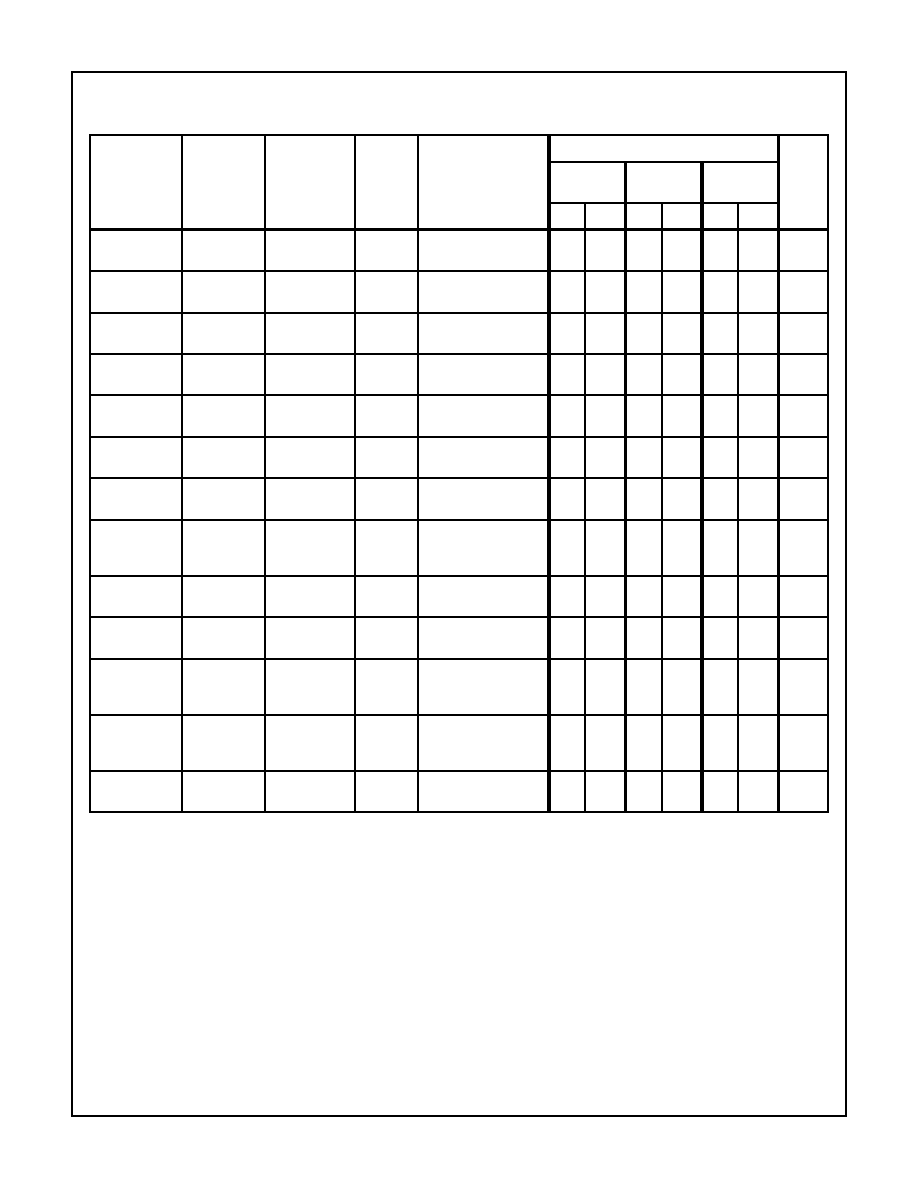
TABLE 1. 65162/883 DC ELECTRICAL PERFORMANCE SPECIFICATIONS
Device Guaranteed and 100% Tested
PARAMETER
SYMBOL
(NOTE 1)
CONDITIONS
GROUP A
SUBGROUPS
TEMPERATURE
LIMITS
UNITS
MIN
MAX
High Level Out-
put Voltage
VOH1
VCC = 4.5V, IO = -1.0mA
1, 2, 3
-55
o
C
T
A
+125
o
C
2.4
-
V
Low Level Output
Voltage
VOL
VCC = 4.5V, IO = 4.0mA
1, 2, 3
-55
o
C
T
A
+125
o
C
-
0.4
V
High Impedance
Output Leakage
Current
IIOZ
VCC = 5.5V, G = 2.2V, or
E = 2.2V, VI/O = GND or VCC
1, 2, 3
-55
o
C
T
A
+125
o
C
-1.0
1.0
µ
A
Input Leakage
Current
II
VCC = 5.5V,
VI = GND or VCC
1, 2, 3
-55
o
C
T
A
+125
o
C
-1.0
1.0
µ
A
Standby Supply
Current
ICCSB1
HM-65162B/883, IO = 0mA,
VCC = 5.5V, E = VCC -0.3V
1, 2, 3
-55
o
C
T
A
+125
o
C
-
50
µ
A
HM-65162/883, IO = 0mA,
VCC = 5.5V, E = VCC - 0.3V
1, 2, 3
-55
o
C
T
A
+125
o
C
-
100
µ
A
HM-65162C/883, IO = 0mA,
VCC = 5.5V, E = VCC - 0.3V
1, 2, 3
-55
o
C
T
A
+125
o
C
-
900
µ
A
Standby Supply
Current
ICCSB
VCC = 5.5V, IO = 0mA,
E = 2.2V
1, 2, 3
-55
o
C
T
A
+125
o
C
-
8
mA
Operating Supply
Current
ICCOP
VCC = 5.5V, G = 5.5V,
(Note 2), f = 1MHz, E = 0.8V
1, 2, 3
-55
o
C
T
A
+125
o
C
-
70
mA
Enable Supply
Current
ICCEN
VCC = 5.5V, IO = 0mA,
E = 0.8V
1, 2, 3
-55
o
C
T
A
+125
o
C
-
70
mA
Data Retention
Supply Current
ICCDR
HM-65162B/883, IO = 0mA,
VCC = 2.0V, E = VCC - 0.3V
1, 2, 3
-55
o
C
T
A
+125
o
C
-
20
µ
A
HM-65162/883, IO = 0mA,
VCC = 2.0V, E = VCC - 0.3V
1, 2, 3
-55
o
C
T
A
+125
o
C
-
40
µ
A
HM-65162C/883, IO = 0mA,
VCC = 2.0V, E = VCC - 0.3V
1, 2, 3
-55
o
C
T
A
+125
o
C
-
300
µ
A
Functional Test
FT
VCC = 4.5V (Note 3)
7, 8A, 8B
-55
o
C
T
A
+125
o
C
-
-
-
NOTES:
1. All voltages referenced to device GND.
2. Input pulse levels: 0.8V to VCC - 2.0V; Input rise and fall times: 5ns (max); Input and output timing reference level: 1.5V; Output load: 1
TTL gate equivalent, CL = 50pF (min) - for CL greater than 50pF, access time by 0.15ns per pF.
3. TAVQV = TELQV + TAVEL.
HM-65162/883
191
TABLE 2. HM-65162/883 AC ELECTRICAL PERFORMANCE SPECIFICATIONS
Device Guaranteed and 100% Tested.
PARAMETER
SYMBOL
(NOTES 1, 2)
CONDITIONS
GROUP
A SUB-
GROUPS
TEMPERA-
TURE
LIMITS
UNITS
HM-65162B
/883
HM-65162
/883
HM-65162C
/883
MIN
MAX
MIN
MAX
MIN
MAX
Read/Write/
Cycle Time
(1) TAVAX
VCC = 4.5V
and 5.5V
9, 10, 11
-55
o
C
T
A
+125
o
C
70
-
90
-
90
-
ns
Address
Access Time
(2) TAVQV
VCC = 4.5V
and 5.5V
9, 10, 11
-55
o
C
T
A
+125
o
C
-
70
-
90
-
90
ns
Chip Enable
Access Time
(3) TELQV
VCC = 4.5V
and 5.5V
9, 10, 11
-55
o
C
T
A
+125
o
C
-
70
-
90
-
90
ns
Output Enable
Access Time
(5) TGLQV
VCC = 4.5V
and 5.5V
9, 10, 11
-55
o
C
T
A
+125
o
C
-
50
-
65
-
65
ns
Chip Selection
to End of Write
(11) TELWH
VCC = 4.5V
and 5.5V
9, 10, 11
-55
o
C
T
A
+125
o
C
45
-
55
-
55
-
ns
Address Setup
Time
(12) TAVWL
VCC = 4.5V
and 5.5V
9, 10, 11
-55
o
C
T
A
+125
o
C
10
-
10
-
10
-
ns
Write Enable
Pulse Write
(13) TWLWH
VCC = 4.5V
and 5.5V
9, 10, 11
-55
o
C
T
A
+125
o
C
40
-
55
-
55
-
ns
Write Enable
Read Setup
Time
(14) TWHAX
VCC = 4.5V
and 5.5V
9, 10, 11
-55
o
C
T
A
+125
o
C
10
-
10
-
10
-
ns
Data Setup
Time
(17) TDVWH
VCC = 4.5V
and 5.5V
9, 10, 11
-55
o
C
T
A
+125
o
C
30
-
30
-
30
-
ns
Data Hold Time (18) TWHDX
VCC = 4.5V
and 5.5V
9, 10, 11
-55
o
C
T
A
+125
o
C
10
-
15
-
15
-
ns
Write Enable
Pulse Setup
Time
(20) TWLEH
VCC = 4.5V
and 5.5V
9, 10, 11
-55
o
C
T
A
+125
o
C
40
-
55
-
55
-
ns
Chip Enable
Data Setup
Time
(21) TDVEH
VCC = 4.5V
and 5.5V
9, 10, 11
-55
o
C
T
A
+125
o
C
30
-
30
-
30
-
ns
Address Valid
to End of Write
(22) TAVWH
VCC = 4.5V
and 5.5V
9, 10, 11
-55
o
C
T
A
+125
o
C
50
-
65
-
65
-
ns
NOTES:
1. All voltages referenced to device GND.
2. Input pulse levels: 0.8V to VCC -2.0V; Input rise and fall times: 5ns (max); Input and output timing reference level: 1.5V; Output load: 1 TTL
gate equivalent, CL = 50pF (min) - for CL greater than 50pF, access time is derated by 0.15ns per pF.
3. TAVQV = TELQV + TAVEL.
HM-65162/883

192
TABLE 3. HM-65162/883 ELECTRICAL PERFORMANCE SPECIFICATIONS, AC AND DC
PARAMETER
SYMBOL
CONDITIONS
NOTES TEMPERATURE
LIMITS
UNITS
HM-
65162B/883
HM-
65162/883
HM-
65162C/883
MIN
MAX
MIN
MAX
MIN
MAX
Input
Capacitance
CIN
VCC = Open,
F = 1MHz, All
Measurements
Referenced To
Device Ground
1, 2
+25
o
C
-
10
-
10
-
10
pF
1, 3
+25
o
C
-
8
-
8
-
8
pF
I/O
Capacitance
CI/O
VCC = Open,
F = 1MHz, All
Measurements
Referenced To
Device Ground
1, 2
+25
o
C
-
12
-
12
-
12
pF
1, 3
+25
o
C
-
10
-
10
-
10
pF
Chip Enable to
Output ON
(4) TELQX
VCC = 4.5V and
5.5V
1
-55
o
C
T
A
+125
o
C
5
-
0
-
5
-
ns
Output Enable
to Output ON
(6) TGLQX
VCC = 4.5V and
5.5V
1
-55
o
C
T
A
+125
o
C
5
-
5
-
5
-
ns
Chip Enable
High to Output
In High Z
(7) TEHQZ
VCC = 4.5V and
5.5V
1
-55
o
C
T
A
+125
o
C
-
35
-
50
-
50
ns
Output Disable
to Output in
High Z
(8) TGHQZ
VCC = 4.5V and
5.5V
1
-55
o
C
T
A
+125
o
C
-
35
-
40
-
40
ns
Output Hold
from Address
Change
(9) TAVQX
VCC = 4.5V and
5.5V
1
-55
o
C
T
A
+125
o
C
5
-
5
-
5
-
ns
Write Enable to
Output in High Z
(16) TWLQZ
VCC = 4.5V and
5.5V
1
-55
o
C
T
A
+125
o
C
-
40
-
50
-
50
ns
Write Enable
High to Output
ON
(19) TWHQX VCC = 4.5V and
5.5V
1
-55
o
C
T
A
+125
o
C
0
-
0
-
0
-
ns
Output High
Voltage
VOH2
VCC = 4.5V,
IO = -100
µ
A
1
-55
o
C
T
A
+125
o
C
VCC
-
0.4V
-
VCC
-
0.4V
-
VCC
-
0.4V
-
V
NOTES:
1. The parameters listed in Table 3 are controlled via design or process parameters and are not directly tested. These parameters are
characterized upon initial design release and upon design changes which would affect these characteristics.
2. Applies to DIP device types only.
3. Applies to LCC device types only.
TABLE 4. APPLICABLE SUBGROUPS
CONFORMANCE GROUPS
METHOD
SUBGROUPS
Initial Test
100%/5004
-
Interim Test
100%/5004
1, 7, 9
PDA
100%/5004
1
Final Test
100%/5004
2, 3, 7, 8A, 8B, 10, 11
Group A
Samples/5005
1, 2, 3, 7, 8A, 8B, 9, 10, 11
Groups C & D
Samples/5005
1, 7, 9
HM-65162/883
