
1
Æ
May 2002
HM-65642
8K x 8 Asynchronous
CMOS Static RAM
Features
∑ Full CMOS Design
∑ Six Transistor Memory Cell
∑ Low Standby Supply Current . . . . . . . . . . . . . . . . 100
µA
∑ Low Operating Supply Current. . . . . . . . . . . . . . . 20mA
∑ Fast Address Access Time . . . . . . . . . . . . . . . . . . 150ns
∑ Low Data Retention Supply Voltage . . . . . . . . . . . 2.0V
∑ CMOS/TTL Compatible Inputs/Outputs
∑ JEDEC Approved Pinout
∑ Equal Cycle and Access Times
∑ No Clocks or Strobes Required
∑ Gated Inputs
∑ No Pull-Up or Pull-Down Resistors Required
∑ Easy Microprocessor Interfacing
∑ Dual Chip Enable Control
Description
The HM-65642 is a CMOS 8192 x 8-bit Static Random
Access Memory. The pinout is the JEDEC 28 pin, 8-bit wide
standard, which allows easy memory board layouts which
accommodate a variety of industry standard ROM, PROM,
EPROM, EEPROM and RAMs. The HM-65642 is ideally
suited for use in microprocessor based systems. In particu-
lar, interfacing with the Intersil 80C86 and 80C88 micropro-
cessors is simplified by the convenient output enable (G)
input.
The HM-65642 is a full CMOS RAM which utilizes an array
of six transistor (6T) memory cells for the most stable and
lowest possible standby supply current over the full military
temperature range.
Ordering Information
PACKAGE
TEMPERATURE
RANGE
(NOTE 1)
150ns/75
µA
(NOTE 1)
150ns/150
µA
(NOTE 1)
200ns/250
µA
PKG. NO.
CERDIP
-40
o
C to +85
o
C
-
HM1-65642-9
-
F28.6
JAN#
-55
o
C to +125
o
C
29205BXA
-
-
F28.6
NOTE:
1. Access Time/Data Retention Supply Current.
Pinout
HM-65642 (CERDIP)
TOP VIEW
28
27
26
25
24
23
22
21
20
19
18
17
16
15
NC
A12
A7
A6
A5
A4
A3
A2
A1
A0
DQ0
DQ1
DQ2
GND
1
2
3
4
5
6
7
8
9
10
11
12
13
14
V
CC
E2
A8
A9
A11
A10
DQ7
DQ6
DQ5
DQ4
DQ3
W
G
E1
PIN
DESCRIPTION
A
Address Input
DQ
Data Input/Output
E1
Chip Enable
E2
Chip Enable
W
Write Enable
G
Output Enable
NC
No Connections
GND
Ground
V
CC
Power
FN3005.2
CAUTION: These devices are sensitive to electrostatic discharge; follow proper IC Handling Procedures.
1-888-INTERSIL or 321-724-7143
|
Intersil (and design) is a registered trademark of Intersil Americas Inc.
Copyright © Intersil Americas Inc. 2002. All Rights Reserved
2
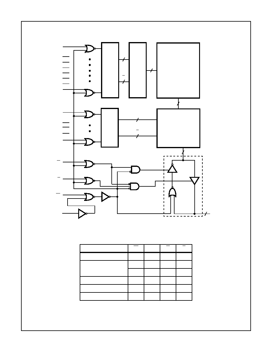
Functional Diagram
TRUTH TABLE
MODE
E1
E2
W
G
Standby (CMOS)
X
GND
X
X
Standby (TTL)
V
IH
X
X
X
X
V
IL
X
X
Enable (High Z)
V
IL
V
IH
V
IH
V
IH
Write
V
IL
V
IH
V
IL
X
Read
V
IL
V
IH
V
IH
V
IL
256
A9
A8
A12
A7
A6
A5
A4
A3
RO
W
ADDRESS BUF
F
E
RS
RO
W
DE
C
O
DER
256 x 256
MEMORY ARRAY
A
8
A
8
256
CO
L
U
M
N
ADDRESS BUF
F
E
RS
COLUMN SELECT
(8 OF 256)
A
5
A
5
8
A2
A1
A0
A10
A11
W
G
E1
E2
1 OF 8
8
DQ
HM-65642
3
Absolute Maximum Ratings
Thermal Information
Supply Voltage . . . . . . . . . . . . . . . . . . . . . . . . . . . . . . . . . . . . . +7.0V
Input or Output Voltage Applied for All Grades . . . . . . GND -0.3V to
V
CC
+0.3V
Typical Derating Factor . . . . . . . . . . . 5mA/MHz Increase in ICCOP
ESD Classification . . . . . . . . . . . . . . . . . . . . . . . . . . . . . . . . Class 1
Thermal Resistance (Typical)
JA
JC
CERDIP Package . . . . . . . . . . . . . . . .
45
o
C/W
8
o
C/W
Maximum Storage Temperature Range . . . . . . . . .-65
o
C to +150
o
C
Maximum Junction Temperature. . . . . . . . . . . . . . . . . . . . . . +175
o
C
Maximum Lead Temperature (Soldering 10s). . . . . . . . . . . . +300
o
C
Die Characteristics
Gate Count . . . . . . . . . . . . . . . . . . . . . . . . . . . . . . . . 101,000 Gates
CAUTION: Stresses above those listed in "Absolute Maximum Ratings" may cause permanent damage to the device. This is a stress only rating and operation
of the device at these or any other conditions above those indicated in the operational sections of this specification is not implied.
Operating Conditions
Operating Voltage Range . . . . . . . . . . . . . . . . . . . . . +4.5V to +5.5V
Operating Temperature Range
HM-65642-9 . . . . . . . . . . . . . . . . . . . . . . . . . . . . . -40
o
C to +85
o
C
Input Low Voltage . . . . . . . . . . . . . . . . . . . . . . . . . . . .-0.3V to +0.8V
Input High Voltage. . . . . . . . . . . . . . . . . . . . . . . +2.2V to V
CC
+0.3V
DC Electrical Specifications
V
CC
= 5V
±10%; T
A
= -40
o
C to +85
o
C (HM-65642-9)
SYMBOL
PARAMETER
LIMITS
UNITS
TEST CONDITIONS
MIN
MAX
ICCSB1
Standby Supply Current (CMOS)
-
250
µA
E2 = GND, V
CC
= 5.5V
ICCSB2
Standby Supply Current (TTL)
-
5
mA
E2 = 0.8V or E1 = 2.2V, V
CC
= 5.5V
ICCDR
Data Retention Supply Current
-
150
µA
E2 = GND, V
CC
= 2.0V
ICCEN
Enabled Supply Current
-
5
mA
E2 = 2.2V, E1 = 0.8V, V
CC
= 5.5V,
IIO = 0mA
ICCOP
Operating Supply Current (Note 1)
-
20
mA
f = 1MHz, E1 = 0.8V, E2 = 2.2V,
V
CC
= 5.5V, IIO = 0mA
II
Input Leakage Current
-1.0
+1.0
µA
VI = V
CC
or GND, V
CC
= 5.5V
IIOZ
Input/Output Leakage Current
-1.0
+1.0
µA
E2 = GND, VIO = V
CC
or GND,
V
CC
= 5.5V
VCCDR
Data Retention Supply Voltage
2.0
-
V
VOH1
Output High Voltage
2.4
-
V
IOH = -1.0mA, V
CC
= 4.5V
VOH2
Output High Voltage (Note 2)
V
CC
-0.4
-
V
IOH = -100
µA, V
CC
= 4.5V
VOL
Output Low Voltage
-
0.4
V
IOL = 4.0mA, V
CC
= 4.5V
Capacitance
T
A
= +25
o
C
SYMBOL
PARAMETER
MAX
UNITS
TEST CONDITIONS
CI
Input Capacitance (Note 2)
12
pF
f = 1MHz, All measurements are
referenced to device GND
CIO
Input/Output Capacitance (Note 2)
14
pF
NOTES:
1. Typical derating 5mA/MHz increase in ICCOP.
2. Tested at initial design and after major design changes.
HM-65642
4
AC Electrical Specifications
V
CC
= 5V
±10%; T
A
= -40
o
C to +85
o
C (HM-65642-9)
SYMBOL
PARAMETER
LIMITS
UNITS
TEST
CONDITIONS
MIN
MAX
READ CYCLE
(1) TAVAX
Read Cycle Time
150
-
ns
(Notes 1, 3)
(2) TAVQV
Address Access Time
-
150
ns
(Notes 1, 3)
(3) TE1LQV
Chip Enable Access Time
E1
-
150
ns
(Notes 2, 3)
(4) TE2HQV
Chip Enable Access Time
E2
-
150
ns
(Notes 1, 3)
(5) TGLQV
Output Enable Access Time
-
70
ns
(Notes 1, 3)
(6) TE1LQX
Chip Enable Valid to Output On
E1
10
-
ns
(Notes 2, 3)
(7) TE2HQX
Chip Enable Valid to Output On
E2
10
-
ns
(Notes 2, 3)
(8) TGLQX
Output Enable Valid to Output On
5
-
ns
(Notes 2, 3)
(9) TE1HQZ
Chip Enable Not Valid to Output Off
E1
-
50
ns
(Notes 2, 3)
(10) TE2LQZ
Chip Enable Not Valid to Output Off
E2
-
60
ns
(Notes 2, 3)
(11) TGHQZ
Output Enable Not Valid to Output Off
-
50
ns
(Notes 2, 3)
(12) TAXQX
Output Hold From Address Change
10
-
ns
(Notes 2, 3)
WRITE CYCLE
(13) TAVAX
Write Cycle Time
150
-
ns
(Notes 1, 3)
(14) TWLWH
Write Pulse Width
90
-
ns
(Notes 1, 3)
(15) TE1LE1H
Chip Enable to End of Write
E1
90
-
ns
(Notes 1, 3)
(16) TE2HE2L
Chip Enable to End of Write
E2
90
-
ns
(Notes 1, 3)
(17) TAVWL
Address Setup Time
Late Write
0
-
ns
(Notes 1, 3)
(18) TAVE1L
Address Setup Time
Early Write
E1
0
-
ns
(Notes 1, 3)
(19) TAVE2H
Address Setup Time
Early Write
E2
0
-
ns
(Notes 1, 3)
(20) TWHAX
Write Recovery Time
Late Write
10
-
ns
(Notes 1, 3)
(21) TE1HAX
Write Recovery Time
Early Write
E1
10
-
ns
(Notes 1, 3)
(22) TE2LAX
Write Recovery Time
Early Write
E2
10
-
ns
(Notes 1, 3)
(23) TDVWH
Data Setup Time
Late Write
60
-
ns
(Notes 1, 3)
(24) TDVE1H
Data Setup Time
Early Write
E1
60
-
-
(Notes 1, 3)
(25) TDVE2L
Data Setup Time
Early Write
E2
60
-
ns
(Notes 1, 3)
(26) TWHDX
Data Hold Time
Late Write
5
-
ns
(Notes 1, 3)
(27) TE1HDX
Data Hold Time
Early Write
E1
10
-
ns
(Notes 1, 3)
(28) TE2LDX
Data Hold Time
Early Write
E2
10
-
ns
(Notes 1, 3)
(29) TWLQZ
Write Enable Low to Output Off
-
50
ns
(Notes 2, 3)
(30) TWHQX
Write Enable High to Output On
5
-
ns
(Notes 2, 3)
NOTES:
1. Input pulse levels: 0V to 3.0V; Input rise and fall times: 5ns (max); Input and output timing reference level: 1.5V; Output load:
1 TTL gate equivalent, C
L
= 50pF (min) - for C
L
greater than 50pF, access time is derated by 0.15ns per pF.
2. Tested at initial design and after major design changes.
3. V
CC
= 4.5V and 5.5V.
HM-65642
5
Low Voltage Data Retention
Intersil CMOS RAMs are designed with battery backup in
mind. Data Retention voltage and supply current are guaran-
teed over the operating temperature range. The following
rules ensure data retention:
1. The RAM must be kept disabled during data retention. This is ac-
complished by holding the E2 pin between -0.3V and GND.
2. During power-up and power-down transitions, E2 must be held
between -0.3V and 10% of V
CC
.
3. The RAM can begin operating one TAVAX after V
CC
reaches the
minimum operating voltage of 4.5V.
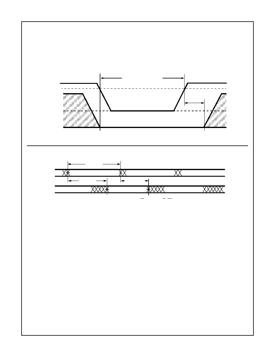
Read Cycles
FIGURE 2. READ CYCLE I: W, E2 HIGH; G, E1 LOW
4.5V
V
CC
V
IH
E2
VCCOR
GND
DATA RETENTION MODE
FIGURE 1. DATA RETENTION
TAVAX
A
ADDRESS 1
Q
TAVAX (1)
TAVQV (2)
TAXQX (12)
ADDRESS 2
DATA 1
DATA 2
HM-65642