
1
February 1998
HS-OP470ARH
Radiation Hardened, Very Low Noise
Quad Operational Amplifier
Features
∑ QML Qualified Per MIL-PRF-38535 Requirements
∑ Radiation Environment
- Total Dose . . . . . . . . . . . . . . . . . . . . . . 1 x 10
5
RAD(Si)
∑ Low Noise
- At 1kHz . . . . . . . . . . . . . . . . . . . . . . . . 4.3nV/
Hz (Typ)
- At 1kHz . . . . . . . . . . . . . . . . . . . . . . . .0.6pA/
Hz (Typ)
∑ Low Offset Voltage. . . . . . . . . . . . . . . . . . . 2.1mV (Max)
∑ High Slew Rate . . . . . . . . . . . . . . . . . . . . . 1.7V/
µ
s (Min)
∑ Gain Bandwidth Product . . . . . . . . . . . . . 8.0MHz (Typ)
Applications
∑ High Q, Active Filters
∑ Voltage Regulators
∑ Integrators
∑ Signal Generators
∑ Voltage References
∑ Space Environments
Description
The HS-OP470ARH is a radiation hardened, monolithic quad
operational amplifier that provides highly reliable performance
in harsh radiation environments. Its excellent noise characteris-
tics coupled with an unique array of dynamic specifications
make this amplifier well-suited for a variety of satellite system
applications. Dielectrically isolated, bipolar processing makes
this device immune to Single Event Latch-up.
The HS-OP470ARH shows almost no change in offset voltage
after exposure to 100K RAD(Si) gamma radiation, with only a
minor increase in current. Complementing these specifications
is a post radiation open loop gain in excess of 40kV/V.
This quad operational amplifier is available in an industry
standard pinout, allowing for immediate interchangeability
with most other quad operational amplifiers.
Specifications for Rad Hard QML devices are controlled
by the Defense Supply Center in Columbus (DSCC).
SMD numbers must be used when ordering.
Detailed Electrical Specifications for this are contained
in SMD 5962-98533. A "hot-link" is provided on our
homepage with instructions for downloading.
http://www.intersil.com/data/sm/index.htm
Ordering Information
Pinout
HS-OP470ARH (FLATPACK)
TOP VIEW
SMD PART NUMBER
INTERSIL PART NUMBER
TEMP. RANGE (
o
C)
PACKAGE
CASE OUTLINE
5962R9853301VXC
HS9-OP470ARH-Q
-55 to 125
14 Ld Flatpack
CDFP3-F14
N/A
HS9-OP470ARH/Sample
25
14 Ld Flatpack
CDFP3-F14
V+
OUT 1
-IN1
+IN1
+IN2
-IN2
OUT 2
V-
OUT 3
OUT 4
-IN3
+IN3
+IN4
-IN4
14
13
12
11
10
9
8
2
3
4
5
6
7
1
File Number
4471
CAUTION: These devices are sensitive to electrostatic discharge; follow proper IC Handling Procedures.
1-888-INTERSIL or 321-724-7143 | Copyright © Intersil Corporation 1999
2
All Intersil semiconductor products are manufactured, assembled and tested under ISO9000 quality systems certification.
Intersil products are sold by description only. Intersil Corporation reserves the right to make changes in circuit design and/or specifications at any time without
notice. Accordingly, the reader is cautioned to verify that data sheets are current before placing orders. Information furnished by Intersil is believed to be accurate
and reliable. However, no responsibility is assumed by Intersil or its subsidiaries for its use; nor for any infringements of patents or other rights of third parties which
may result from its use. No license is granted by implication or otherwise under any patent or patent rights of Intersil or its subsidiaries.
For information regarding Intersil Corporation and its products, see web site http://www.intersil.com
Sales Office Headquarters
NORTH AMERICA
Intersil Corporation
P. O. Box 883, Mail Stop 53-204
Melbourne, FL 32902
TEL: (321) 724-7000
FAX: (321) 724-7240
EUROPE
Intersil SA
Mercure Center
100, Rue de la Fusee
1130 Brussels, Belgium
TEL: (32) 2.724.2111
FAX: (32) 2.724.22.05
ASIA
Intersil (Taiwan) Ltd.
Taiwan Limited
7F-6, No. 101 Fu Hsing North Road
Taipei, Taiwan
Republic of China
TEL: (886) 2 2716 9310
FAX: (886) 2 2715 3029
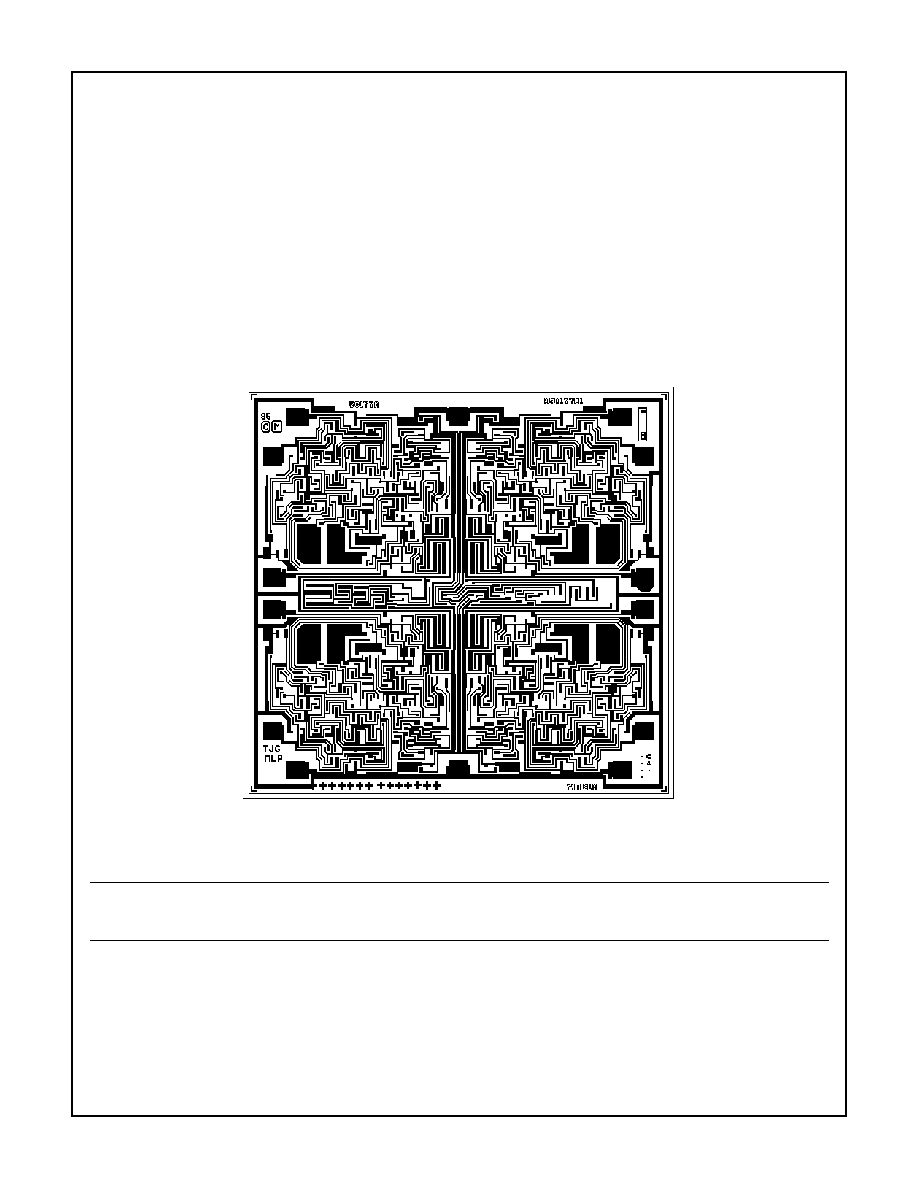
Metallization Mask Layout
DIE DIMENSIONS:
95 mils x 99 mils x 19 mils
±
1 mil
(2420
µ
m x 2530
µ
m x 483
µ
m
±
25.4
µ
m)
METALLIZATION:
Type: Al, 1% Cu
Thickness: 16k
≈
±
2k
≈
SUBSTRATE POTENTIAL (Powered Up):
Unbiased
BACKSIDE FINISH:
Silicon
PASSIVATION:
Type: Nitride (SI3N4) over Silox (SIO2, 5% Phos.)
Silox Thickness: 12k
≈
±
2k
≈
Nitride Thickness: 3.5k
≈
±
1.5k
≈
WORST CASE CURRENT DENSITY:
<2.0 x 10
5
A/cm
2
TRANSISTOR COUNT:
175
PROCESS:
Bipolar Dielectric Isolation
+IN2
V+
+IN1
-IN1
OUT1
OUT4
-IN4
-IN3
OUT3
OUT2
-IN2
+IN4
V-
+IN3
HS-OP470ARH