1
TM
FN2485.7
HSP45116
Numerically Controlled
Oscillator/Modulator
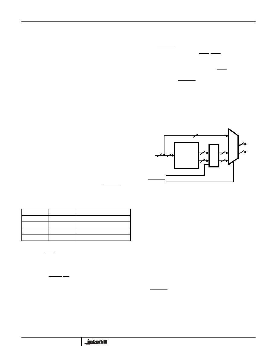
The Intersil HSP45116 combines a high performance
quadrature Numerically Controlled Oscillator (NCO) and a
high speed 16-bit Complex Multiplier/Accumulator (CMAC)
on a single IC. This combination of functions allows a
complex vector to be multiplied by the internally generated
(cos, sin) vector for quadrature modulation and
demodulation. As shown in the Block Diagram, the
HSP45116 is divided into three main sections. The
Phase/Frequency Control Section (PFCS) and the
Sine/Cosine Section together form a complex NCO. The
CMAC multiplies the output of the Sine/ Cosine Section with
an external complex vector.
The inputs to the Phase/Frequency Control Section consist
of a microprocessor interface and individual control lines.
The phase resolution of the PFCS is 32 bits, which results in
frequency resolution better than 0.008Hz at 33MHz. The
output of the PFCS is the argument of the sine and cosine.
The spurious free dynamic range of the complex sinusoid is
greater than 90dBc.
The output vector from the Sine/Cosine Section is one of the
inputs to the Complex Multiplier/Accumulator. The CMAC
multiplies this (cos, sin) vector by an external complex vector
and can accumulate the result. The resulting complex vectors
are available through two 20-bit output ports which maintain
the 90dB spectral purity. This result can be accumulated
internally to implement an accumulate and dump filter.
A quadrature down converter can be implemented by
loading a center frequency into the Phase/Frequency
Control Section. The signal to be down converted is the
Vector Input of the CMAC, which multiplies the data by the
rotating vector from the Sine/Cosine Section. The resulting
complex output is the down converted signal.
Features
∑ NCO and CMAC on One Chip
∑ 15MHz, 25.6MHz, 33MHz Versions
∑ 32-Bit Frequency Control
∑ 16-Bit Phase Modulation
∑ 16-Bit CMAC
∑ 0.008Hz Tuning Resolution at 33MHz
∑ Spurious Frequency Components < -90dBc
∑ Fully Static CMOS
Applications
∑ Frequency Synthesis
∑ Modulation - AM, FM, PSK, FSK, QAM
∑ Demodulation, PLL
∑ Phase Shifter
∑ Polar to Cartesian Conversions
Block Diagram
Ordering Information
PART NUMBER
TEMP.
RANGE (
o
C)
PACKAGE
PKG. NO.
HSP45116VC-15
0 to 70
160 Ld MQFP Q160.28x28
HSP45116VC-25
0 to 70
160 Ld MQFP Q160.28x28
HSP45116GC-15
0 to 70
145 Ld CPGA G145.A
HSP45116GC-25
0 to 70
145 Ld CPGA G145.A
HSP45116GC-33
0 to 70
145 Ld CPGA G145.A
HSP45116GI-15
-40 to 85
145 Ld CPGA G145.A
HSP45116GI-25
-40 to 85
145 Ld CPGA G145.A
HSP45116GI-33
-40 to 85
145 Ld CPGA G145.A
HSP45116GM-15/883
-55 to 125
145 Ld CPGA G145.A
HSP45116GM-25/883
-55 to 125
145 Ld CPGA G145.A
HSP45116AVC-52
0 to 70
160 Ld MQFP Q160.28x28
This part has its own data sheet under HSP45116A,
Document # FN4156.
PHASE/
FREQUENCY
CONTROL
SECTION
SINE/
COSINE
SECTION
CMAC
SINE/
COSINE
ARGUMENT
SIN
COS
VECTOR INPUT
VECTOR OUTPUT
R
I
R
I
MICROPROCESSOR
INTERFACE
INDIVIDUAL
CONTROL SIGNALS
Data Sheet
May 1999
CAUTION: These devices are sensitive to electrostatic discharge; follow proper IC Handling Procedures.
1-888-INTERSIL or 321-724-7143
|
Intersil (and design) is a trademark of Intersil Americas Inc.
Copyright © Intersil Americas Inc. 2002. All Rights Reserved
2
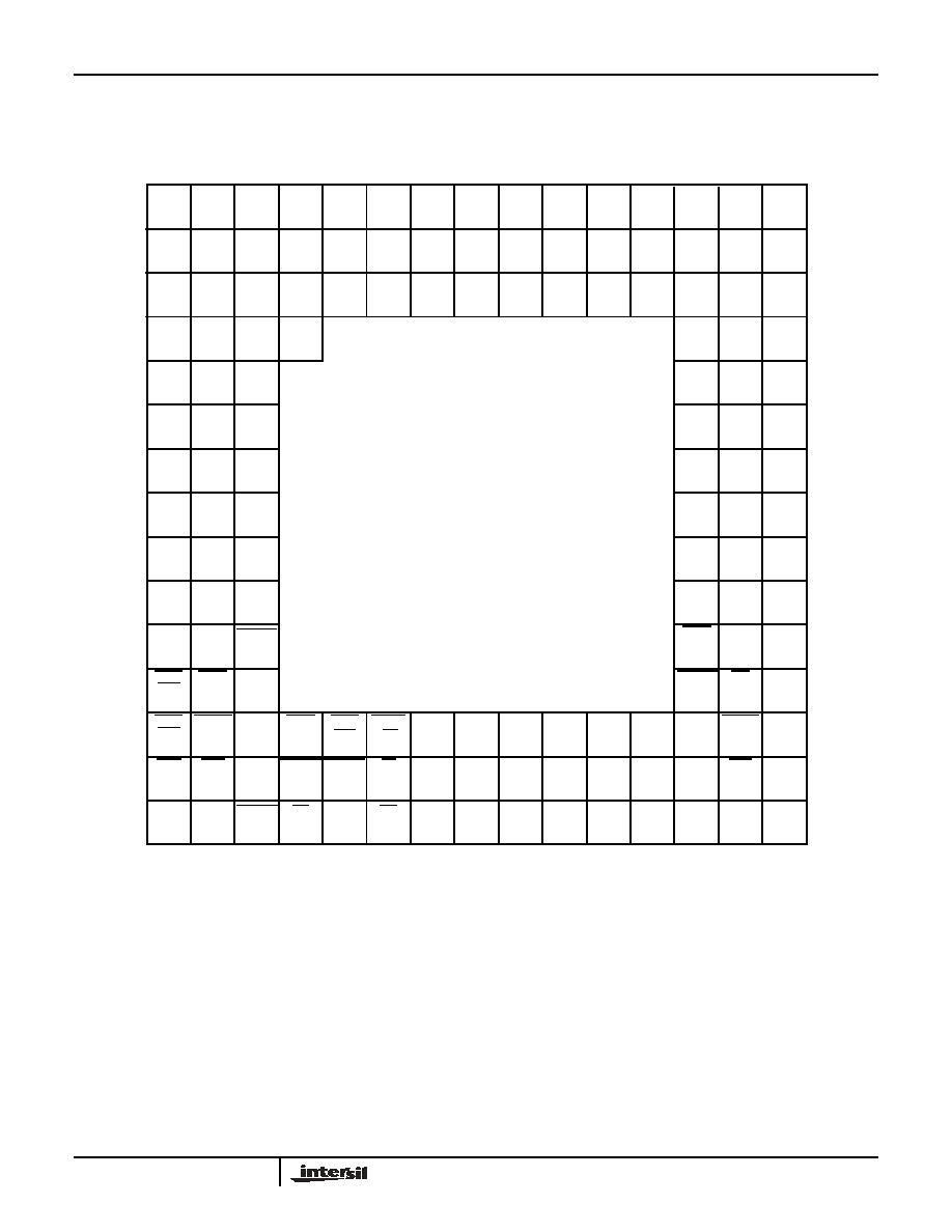
Pinouts
145 PIN PGA
TOP VIEW
A
B
C
D
E
F
G
H
J
K
L
M
N
P
Q
A
B
C
D
E
F
G
H
J
K
L
M
N
P
Q
1
2
3
4
5
6
7
8
9
10
11
12
13
14
15
1
2
3
4
5
6
7
8
9
10
11
12
13
14
15
GND
V
CC
V
CC
V
CC
GND
GND
GND
GND
V
CC
V
CC
GND
V
CC
GND
IMIN
IMIN
IMIN
IMIN
IMIN
IMIN
IMIN
IMIN
INDEX
RIN
RIN
RIN
RIN
RIN
RIN
RIN
RIN
RIN
RIN
ACC
CLK
AD
1
C
15
C
10
MOD
0
ENOF
REG
AD
0
C
14
C
13
C
8
C
2
0
3
1
4
6
5
9
8
7
11
12
2
3
6
12
5
7
10
13
PACO
RO
1
RO
5
RO
8
RO
9
RO
14
IO
0
IO
3
RO
18
IO
2
IO
10
IO
1
IO
4
RO
19
RO
17
RO
16
RO
15
RO
13
RO
11
RO
12
RO
10
RO
7
RO
4
RO
6
RO
2
DET
1
RO
3
OEREXT
OEI
RO
0
OEIEXT
DET
0
1
C
3
C
1
OER
C
5
C
4
C
0
TICO
PACI
BINFMT
PEAK
ENPH
REG
MOD
1
LOAD
CLROFR
ENI
ENCF
REG
ENTIREG
WR
CS
MODPI
/2PI
C
6
C
7
C
11
C
12
SH
1
RBYTILD
RIN
0
RIN
2
SH
0
PMSEL
ENPHAC
C
9
IMIN
17
IMIN
18
IO
17
IO
13
IO
9
IO
6
IO
5
IO
7
IO
8
IO
11
IO
14
IO
16
IO
19
IMIN
14
IO
18
IO
15
IO
12
V
CC
GND
V
CC
IMIN
16
IMIN
4
IMIN
8
IMIN
9
IMIN
11
IMIN
15
IMIN
1
RIN
18
RIN
15
RIN
17
RIN
13
IMIN
0
RIN
10
RIN
14
RIN
16
OUT-
MUX
OUT-
MUX
HSP45116

3
145 PIN PGA
BOTTOM VIEW
Pinouts
(Continued)
A
B
C
D
E
F
G
H
J
K
L
M
N
P
Q
A
B
C
D
E
F
G
H
J
K
L
M
N
P
Q
1
2
3
4
5
6
7
8
9
10
11
12
13
14
15
1
2
3
4
5
6
7
8
9
10
11
12
13
14
15
GND
V
CC
V
CC
V
CC
GND
GND
GND
GND
V
CC
V
CC
GND
V
CC
GND
IMIN
IMIN
IMIN
IMIN
IMIN
IMIN
IMIN
IMIN
INDEX
RIN
RIN
RIN
RIN
RIN
RIN
RIN
RIN
RIN
RIN
ACC
CLK
AD
1
C
15
C
10
MOD
0
ENOF
REG
AD
0
C
14
C
13
C
8
C
2
0
3
1
4
6
5
9
8
7
11
12
2
3
6
12
5
7
10
13
PACO
RO
1
RO
5
RO
8
RO
9
RO
14
IO
0
IO
3
RO
18
IO
2
IO
10
IO
1
IO
4
RO
19
RO
17
RO
16
RO
15
RO
13
RO
11
RO
12
RO
10
RO
7
RO
4
RO
6
RO
2
DET
1
RO
3
OEREXT
OEI
RO
0
OEIEXT
DET
0
1
C
3
C
1
OER
C
5
C
4
C
0
TICO
PACI
BINFMT
PEAK
ENPH
REG
MOD
1
LOAD
CLROFR
ENI
ENCF
REG
ENTIREG
WR
CS
MODPI
/2PI
C
6
C
7
C
11
C
12
SH
1
RBYTILD
RIN
0
RIN
2
SH
0
PMSEL
ENPHAC
C
9
IMIN
17
IMIN
18
IO
17
IO
13
IO
9
IO
6
IO
5
IO
7
IO
8
IO
11
IO
14
IO
16
IO
19
IMIN
14
IO
18
IO
15
IO
12
V
CC
GND
V
CC
IMIN
16
IMIN
4
IMIN
8
IMIN
9
IMIN
11
IMIN
15
IMIN
1
RIN
18
RIN
15
RIN
17
RIN
13
IMIN
0
RIN
10
RIN
14
RIN
16
OUT-
MUX
OUT-
MUX
HSP45116
4
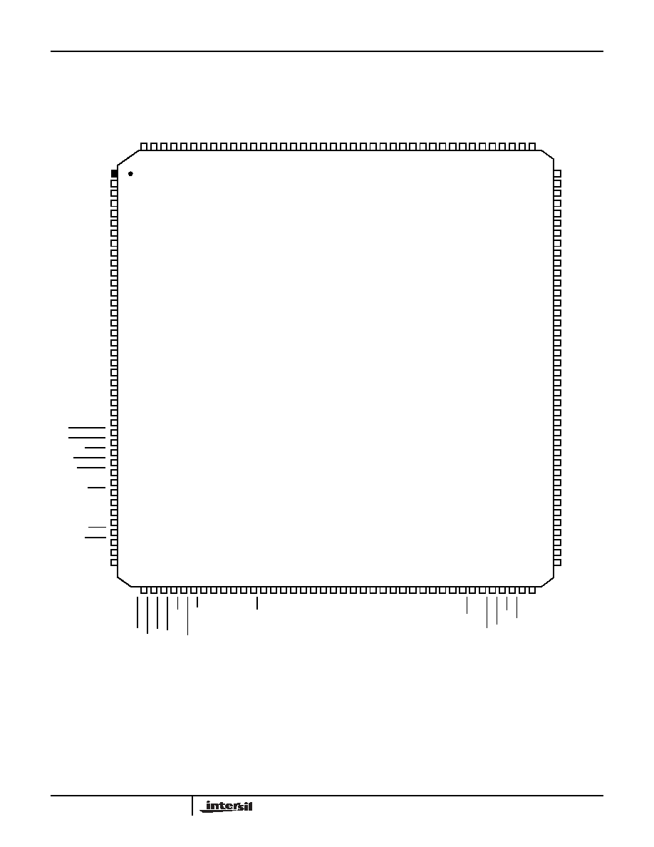
160LEAD MQFP
TOP VIEW
Pinouts
(Continued)
2
1
3
4
5
6
7
8
9
10
11
12
13
14
15
16
17
18
19
20
21
22
23
24
25
26
27
28
29
30
31
32
33
34
35
36
37
38
39
40
119
120
118
117
116
115
114
113
112
111
110
109
108
107
106
105
104
103
102
101
100
99
98
97
96
95
94
93
92
91
90
89
88
87
86
85
84
83
82
81
41
43
44
45
46
47
48
49
50
51
52
53
54
55
56
57
58
59
60
61
62
63
64
65
66
67
68
69
70
71
72
73
74
75
76
77
78
79
80
12
6
12
7
12
8
12
9
13
0
13
1
12
1
12
2
12
3
12
4
12
5
13
7
13
8
13
9
14
0
13
2
13
3
13
4
13
5
13
6
14
6
14
7
14
8
14
9
15
0
15
1
14
1
14
2
14
3
14
4
14
5
15
7
15
8
15
9
16
0
15
2
15
3
15
4
15
5
15
6
RO9
V
CC
RO8
RO7
RO6
RO5
GND
RO10
RO18
RO17
RO16
RO15
V
CC
RO13
RO12
RO11
GND
RO14
GND
IO6
IO5
IO4
IO3
IO2
IO1
V
CC
IO0
RO19
GND
GND
RO2
RO1
RO0
DET1
DET0
GND
V
CC
RO4
RO3
NC
CL
ROF
R
ENCF
REG
ENPHAC
ENT
I
REG
ENI
M
O
DP
I/2P
I
CS
GN
D
CL
K
V
CC
AD1
AD0
WR
C1
5
C1
4
C1
3
C1
2
C1
1
C1
0
C9
C8
GN
D
C7
C6
C5
C4
C3
C2
C1
C0
NC
OUT
M
UX
1
OUT
M
UX
0
GN
D
OE
R
V
CC
O
E
REXT
OE
IE
X
T
OE
I
P
ACO
MOD1
V
CC
TICO
GND
RBYTILD
MOD0
PACI
LOAD
PMSEL
NC
PEAK
RIN0
V
CC
SH1
SH0
ACC
ENPHREG
ENOFREG
BINFMT
RIN6
RIN7
RIN8
RIN9
RIN11
RIN5
RIN4
RIN3
RIN2
GND
RIN12
RIN17
RIN18
IMIN0
RIN16
RIN15
RIN14
GND
RIN13
RIN10
IO7
IO8
IO9
V
CC
GND
IO1
0
IO1
1
IO1
2
IO1
3
IO1
4
GND
V
CC
IO1
5
IO1
6
IO1
7
IO1
8
IO1
9
IMI
N
18
IMI
N
17
IMI
N
16
IMI
N
15
IMI
N
14
GND
IMI
N
13
V
CC
IMI
N
12
IMI
N
1
1
IMI
N
10
IMI
N
9
NC
IMI
N
8
IMI
N
7
IMI
N
6
IMI
N
5
IMI
N
4
IMI
N
3
IMI
N
2
GND
IMI
N
1
V
CC
RIN1
42
HSP45116
5
Pin Description
NAME
NUMBER
TYPE
DESCRIPTION
V
CC
A1, A9, A15, G1,
J15, Q1, Q7, Q15
-
+5V Power supply input.
GND
A8, A14, B1, H1,
H15, P15, Q2, Q8
-
Power supply ground input.
C0-15
N8-11, P8-13,
Q9-14
I
Control input bus for loading phase and frequency data into the PFCS. C15 is the MSB.
AD0-1
N7, P7
I
Address pins for selecting destination of C0-15 data.
CS
P6
I
Chip Select (active low).
WR
Q6
I
Write Enable. Data is clocked into the register selected by AD0-1 on the rising edge of WR when
the CS line is low.
CLK
Q5
I
Clock. All registers, except the control registers clocked with WR, are clocked (when enabled)
by the rising edge of CLK.
ENPHREG
M1
I
Phase Register Enable (active low). Registered on chip by CLK. When active, after being
clocked onto chip, ENPHREG enables the clocking of data into the phase register.
ENOFREG
N1
I
Frequency Offset Register Enable (active Low). Registered on chip by CLK. When active, after
being clocked onto chip, ENOFREG enables clocking of data into the frequency offset register.
ENCFREG
N5
I
Center Frequency Register Enable (active low). Registered on chip by CLK. When active, after
being clocked onto chip, ENCFREG enables clocking of data into the center frequency register.
ENPHAC
Q3
I
Phase Accumulator Register Enable (active low). Registered on chip by CLK. When active, after
being clocked onto chip, ENPHAC enables clocking of the phase accumulator register.
ENTIREG
P5
I
Time Interval Control Register Enable (active low). Registered on chip by CLK. When active,
after being clocked onto chip, ENTIREG enables clocking of data into the time accumulator
register.
ENI
Q4
I
Real and Imaginary Data Input Register (RIR, IIR) Enable (active low). Registered on chip by
CLK. When active, after being clocked onto chip, ENI enables clocking of data into the real and
imaginary input data register.
MODPI/2PI
N6
I
Modulo
/2
Select. When low, the Sine and Cosine ROMs are addressed modulo 2
(360
degrees). When high, the most significant address bit is held low so that the ROMs are
addressed modulo
(180 degrees). This input is registered on chip by clock.
CLROFR
P4
I
Frequency Offset Register Output Zero (active low). Registered on chip by CLK. When active,
after being clocked onto chip, CLROFR zeros the data path from the frequency offset register to
the frequency adder. New data can still be clocked into the frequency offset register; CLROFR
does not affect the contents of the register.
LOAD
N4
I
Phase Accumulator Load Control (active low). Registered on chip by CLK. Zeroes feedback
path in the phase accumulator without clearing the phase accumulator register.
MOD0-1
M3, N3
I
External Modulation Control Bits. When selected with the PMSEL line, these bits add a 0, 90,
180, or 270 degree offset to the current phase in the phase accumulator. The lower 14 bits of
the phase control path are set to zero.
These bits are loaded into the phase register when ENPHREG is low.
PMSEL
P3
I
Phase Modulation Select Line. This line determines the source of the data clocked into the phase
register. When high, the phase control register is selected. When low, the external modulation pins
(MOD0-1) are selected for the most significant two bits and the least significant two bits and the
least significant 14 bits are set to zero. This control is registered by CLK.
RBYTILD
L3
I
ROM Bypass, Timer Load. Active low, registered by CLK. This input bypasses the sine/ cosine
ROM so that the 16-bit phase adder output and lower 16 bits of the phase accumulator go
directly to the CMAC's sine and cosine inputs, respectively. It also enables loading of the timer
accumulator register by zeroing the feedback in the accumulator.
PACI
P2
I
Phase Accumulator Carry Input (active low). A low on this pin causes the phase accumulator to
increment by one, in addition to the values in the phase accumulator register and frequency
adder.
HSP45116
6
PACO
L13
O
Phase Accumulator Carry Output. Active low and registered by CLK. A low on this output
indicates that the phase accumulator has overflowed, i.e., the end of one sine/cosine cycle has
been reached.
TICO
P1
O
Time Interval Accumulator Carry Output. Active low, registered by CLK. This output goes low
when a carry is generated by the time interval accumulator. This function is provided to time out
control events such as synchronizing register clocking to data timing.
RIN0-18
C1, C2, D1, D2, E1-
3, F1-3, G2, G3,
H2, H3, J1-3, K1,
K2
I
Real Input Data Bus. This is the external real component into the complex multiplier. The bus is
clocked into the real input data register by CLK when ENI is asserted; two's complement.
IMIN0-18
A2-7, B2-7, C3-8,
D3
I
Imaginary Input Data Bus. This is the external imaginary component into the complex multiplier.
The bus is clocked into the real input data register by CLK when ENI is asserted; two's
complement.
SH0-1
K3, L1
I
Shift Control Inputs. These lines control the input shifters of the RIN and IIN inputs of the
complex multiplier. The shift controls are common to the shifters on both of the busses.
ACC
L2
I
Accumulate/Dump Control. This input controls the complex accumulators and their holding
registers. When high, the accumulators accumulate and the holding registers are disabled.
When low, the feedback in the accumulators is zeroed to cause the accumulators to load.
The holding registers are enabled to clock in the results of the accumulation. This input is
registered by CLK.
BINFMT
N2
I
This input is used to convert the two's complement output to offset binary (unsigned) for
applications using D/A converters. When low, bits RO19 and IO19 are inverted from the internal
two's complement representation. This input is registered by CLK.
PEAK
M2
I
This input enables the peak detect feature of the block floating point detector. When high, the
maximum bit growth in the output holding registers is encoded and output on the DET0-1 pins.
When the PEAK input is asserted, the block floating point detector output will track the maximum
growth in the holding registers, including the data in the holding registers at the time that PEAK
is activated.
OUTMUX0-1
N12, N13
I
These inputs select the data to be output on RO0-19 and IO0-19.
RO0-19
C15, D14, D15,
E14, E15, F13-15,
G13-15, H13, H14,
J13, J14, K13-15,
L15, M15
O
Real Output Data Bus. These Three-state outputs are controlled by OER and OEREXT.
OUTMUX0-1 select the data output on the bus.
IO0-19
A10-13, B8-15, C9-
14, D13, E13
O
Imaginary Output Data Bus. These Three-state outputs are controlled by OEI and OEIEXT.
OUTMUX0-1 select the data output on the bus.
DET0-1
N15, L14
O
These output pins indicate the number of bits of growth in the accumulators. While PEAK is low,
these pins indicate the peak growth. The detector examines bits 15-18, real and imaginary
accumulator holding registers and bits 30-33 of the real and imaginary CMAC holding registers.
The bits indicate the largest growth of the four registers.
OER
P14
I
Three-state control for bits RO0-15. Outputs are enabled when the line is low.
OEREXT
M13
I
Three-state control for bits RO16-19. Outputs are enabled when the line is low.
OEI
M14
I
Three-state control for bits IO0-15. Outputs are enabled when the line is low.
OEIEXT
N14
I
Three-state control for bits IO16-19. Outputs are enabled when the line is low.
Pin Description
(Continued)
NAME
NUMBER
TYPE
DESCRIPTION
HSP45116
7
Functional Block Diagram
CO
S
SI
N
16
R.RBYT
I
L
D
R.
PM
SEL
R.ENPHREG
R
E
G
>
CL
K
16
P
ACI
32
PHASE
INP
U
T
RE
GIS
T
E
R
MS
I
N
P
U
T
RE
GIS
T
E
R
16
14
PHEN
0
16
R.ENPHREG
L
S
INP
U
T
REG
I
ST
ER
LSE
N
O
F
F
SET
REGI
S
T
ER
CENT
E
R
F
R
EQUENCY
RE
GIS
T
E
R
R.PM
S
E
L
F
R
E
Q
UENCY
ADDER
A
D
D
E
R
2
16
PHASE
RE
GIS
T
E
R
16
16
32
32
32
32
R.
CL
RO
F
R
32
32
32
M
SEN
CL
K
32
R.
ENC
F
REG
R.L
O
AD
R.ENOF
RE
G
0
0
MO
D
(
1:
0)
ENCODE
C
(
15:
0)
PHASE
ACCUM
UL
A
T
O
R
ADDER
0
PHASE
ADDER
SIN/CO
S
AR
G
U
M
E
N
T
A
D
D
E
R
32
16
M
S
B
s
16
16
LS
B
s
P
ACO
R.M
O
DPI/2
PI
MS
B
15
R.ENPHAC
A
D
D
E
R
32
PHASE
A
CCUM
UL
A
T
OR
RE
GIS
T
E
R
PH
A
S
E
ACCUM
UL
A
T
OR
DE
C
O
DER
R.ENCF
REG
R.ENOF
REG
R.CL
ROF
R
R.L
O
AD
R.ENPHAC
R.M
O
DPI/2
PI
PM
SE
L
ENCF
REG
CL
ROF
R
LO
A
D
ENPHREG
ENPHAC
M
O
DP
I/2
P
I
ENO
F
REG
CL
K
TI
ME
INCREM
E
NT
32
0
R.ENT
I
REG
3
2
32
32
CARR
Y OUT
TI
ME
ACCUM
UL
A
T
OR
RE
GIS
T
E
R
R.RBYT
I
L
D
TI
C
O
ADDER
32
AD(
1
:
0
)
CS
WR
ENTI
REG
RB
Y
T
IL
D
R.ENT
I
RE
G
ACC
R.ENI
ENI
R.BINF
M
T
BINF
M
T
R.SH(
1
:
0
)
SH(
1
:
0
)
PE
AK
R.
PEAK
S
I
NE
/COS
IN
E
G
E
NE
RA
T
O
R
20
32
32
16
16
16
T
I
M
E
A
CCUM
UL
A
T
OR
OUT
M
UX
(
1
:0
)
O
E
REXT
OE
R
OE
IE
X
T
OE
I
TI
C
O
P
ACO
RIN(
1
8
:
0
)
IM
IN(1
8:0
)
CL
K
PHASE
R.AC
C
R.
E
N
I
R.BI
NF
M
T
R
.
S
H
(1
:0)
R.
PEAK
R.ACC
F
R
EQU
E
NCY
R
E
G
>
R
E
G
>
R
E
G
>
R
E
G
>
R
E
G
>
CL
K
R
E
G
>
CL
K
R
E
G
>
CL
K
R
E
G
>
CL
K
CL
K
R
E
G
>
R
E
G
>
CL
K
CL
K
R
E
G
>
R
E
G
>
CL
K
R
E
G
>
CL
K
P
ACI
R
E
G
>
0 1
MUX
1 0
MUX
0 1
MUX
0 1
MUX
1 0
MUX
RIN(
1
8
:
0
)
IM
IN(1
8:0
)
HSP4
51
1
6
8
Functional Block Diagram
(Continued)
3
ADDER
R1
.ACC
0
0
16
16
SHI
F
T
E
R
SHI
F
T
E
R
R
.
S
H
(1
:0)
R.ENI
19
19
SI
N
16
COS
16
COM
P
L
E
X
MU
L
T
IP
L
I
E
R
33
33
ADDER
ADDER
0
ADDER
COM
P
L
E
X
ACCUM
UL
A
T
OR
CM
AC
ACCUM
UL
A
T
O
R
R.
PEAK
0
GR
O
W
T
H
DET
E
CT
DET
(
1
:
0
)
16
3
FM
T
16
4
OU
TM
U
X
(1
:0)
R
O
(19
-
1
6
)
R
O(
15:
0)
R.BINF
M
T
OE
RE
X
T
OE
R
16
FM
T
16
4
OUT
M
UX
(
1
:0
)
I
O
(1
9-1
6
)
IO(
15
:0)
R.BINF
M
T
OE
IE
X
T
OE
I
35
35
20
20
R1.ACC
R2.ACC
RO
UND
0
RO
UND
RIN0
-
1
8
I
M
I
N0
-
1
8
R.RBYT
I
L
D
R.
E
N
I
R.SH(1:0)
SI
N
COS
R.ACC
R.
PEAK
R.SH(
1
:
0
)
R.ENI
O
U
TMU
X
(1
:0
)
S
e
e T
a
bl
e 4
CL
K
R
E
G
>
CL
K
R
E
G
>
REG
>
CL
K
RE
G
>
CL
K
REG
>
CL
K
REG
>
CL
K
R
E
G
>
CL
K
R
E
G
>
CL
K
REG
>
CL
K
REG
>
CL
K
REG
>
CL
K
CL
K
REG
<
REG
>
CL
K
CL
K
REG
<
REG
>
CL
K
REG
>
CL
K
REG
<
CL
K
REG
>
CL
K
REG
<
CL
K
0
1
MU
X
1
0
MU
X
MU
X
0
1
MU
X
0
1
MU
X
MU
X
O
U
TM
U
X
(1
:0)
S
e
e T
a
b
l
e 4
1 0
MUX
CL
K
RE
G
<
CL
K
RE
G
<
1
0
MU
X
PHASE
R
I
N
(
18:
0)
IM
IN(1
8:
0)
HSP4
51
1
6
9
Functional Description
The Numerically Controlled Oscillator/Modulator (NCOM)
produces a digital complex sinusoid waveform whose
amplitude, phase and frequency are controlled by a set of
input command words. When used as a Numerically
Controlled Oscillator (NCO), it generates 16-bit sine and
cosine vectors at a maximum sample rate of 33MHz. The
NCOM can be preprogrammed to produce a constant (CW)
sine and cosine output for Direct Digital Synthesis (DDS)
applications. Alternatively, the phase and frequency inputs
can be updated in real time to produce a FM, PSK, FSK, or
MSK modulated waveform. The Complex Multiplier/
Accumulator (CMAC) can be used to multiply this waveform
by an input signal for AM and QAM signals. By stepping the
phase input, the output of the ROM becomes an FFT twiddle
factor; when data is input to the Vector Inputs (see Block
Diagram), the NCOM calculates an FFT butterfly.
As shown in the Block Diagram, the NCOM consists of three
parts: Phase and Frequency Control Section (PFCS),
Sine/Cosine Generator, and CMAC. The PFCS stores the
phase and frequency inputs and uses them to calculate the
phase angle of a rotating complex vector. The Sine/Cosine
Generator performs a lookup on this phase and outputs the
appropriate values for the sine and cosine. The sine and
cosine form one set of inputs to the CMAC, which multiplies
them by the input vector to form the modulated output.
Phase and Frequency Control Section
The phase and frequency of the internally generated sine
and cosine are controlled by the PFCS (Block Diagram). The
PFCS generates a 32-bit word that represents the current
phase of the sine and cosine waves being generated; the
Sine/ Cosine Argument. Stepping this phase angle from 0
through full scale (2
32
- 1) corresponds to the phase angle of
a sinusoid starting at 0
o
and advancing around the unit circle
counterclockwise. The PFCS automatically increments the
phase by a preprogrammed amount on every rising edge of
the external clock. The value of the phase step (which is the
sum of the Center and Offset Frequency Registers) is:
The PFCS is divided into two sections: the Phase
Accumulator uses the data on C0-15 to compute the phase
angle that is the input to the Sine/Cosine Section
(Sine/Cosine Argument); the Time Accumulator supplies a
pulse to mark the passage of a preprogrammed period of
time.
The Phase Accumulator and Time Accumulator work on the
same principle: a 32-bit word is added to the contents of a
32-bit accumulator register every clock cycle; when the sum
causes the adder to overflow, the accumulation continues
with the 32 bits of the adder going into the accumulator
register. The overflow bit is used as an output to indicate the
timing of the accumulation overflows. In the Time
Accumulator, the overflow bit generates TICO, the Time
Accumulator carry out (which is the only output of the Time
Accumulator). In the Phase Accumulator, the overflow is
inverted to generate the Phase Accumulator Carry Out,
PACO.
The output of the Phase Accumulator goes to the Phase
Adder, which adds an offset to the top 16 bits of the phase.
This 32-bit number forms the argument of the sine and
cosine, which is passed to the Sine/Cosine Generator.
Both accumulators are loaded 16 bits at a time over the
C0-15 bus. Data on C0-15 is loaded into one of the three
input registers when CS and WR are low. The data in the
Most Significant Input Register and Least Significant Input
Register forms a 32-bit word that is the input to the Center
Frequency Register, Offset Frequency Register and Time
Accumulator. These registers are loaded by enabling the
proper register enable signal; for example, to load the
Center Frequency Register, the data is loaded into the LS
and MS Input Registers, and ENCFREG is set to zero; the
next rising edge of CLK will pass the registered version of
ENCFREG, R.ENCFREG, to the clock enable of the Center
Frequency Register; this register then gets loaded on the
following rising edge of CLK. The contents of the Input
Registers will be continuously loaded into the Center
Frequency Register as long as R.ENCFREG is low.
The Phase Register is loaded in a similar manner. Assuming
PMSEL is high, the contents of the Phase Input Register is
loaded into the Phase Register on every rising clock edge
that R.ENPHREG is low. If PMSEL is low, MOD0-1 supply
the two most significant bits into the Phase Register (MOD1
is the MSB) and the least significant 14 bits are loaded with
0. MOD0-1 are used to generate a Quad Phase Shift Keying
(QPSK) signal (Table 2).
The Phase Accumulator consists of registers and adders
that compute the value of the current phase at every clock. It
has three inputs: Center Frequency, which corresponds to
the carrier frequency of a signal; Offset Frequency, which is
the deviation from the Center Frequency; and Phase, which
Phase Step =
Signal Frequency
Clock Frequency
----------------------------------------------
2
32
◊
TABLE 1. AD0-1 DECODING
AD1
AD0
CS
WR
FUNCTION
0
0
0
Load least significant bits
of frequency input.
0
1
0
Load most significant bits
of frequency input.
1
0
0
Load phase register.
1
1
X
X
Reserved.
X
X
1
X
No Operation.
HSP45116
10
is a 16-bit number that is added to the current phase for PSK
modulation schemes. These three values are used by the
Phase Accumulator and Phase Adder to form the phase of
the internally generated sine and cosine.
The sum of the values in Center and Offset Frequency
Registers corresponds to the desired phase increment
(modulo 2
32
) from one clock to the next. For example,
loading both registers with zero will cause the Phase
Accumulator to add zero to its current output; the output of
the PFCS will remain at its current value; i.e., the output of
the NCOM will be a DC signal. If a hexadecimal 00000001 is
loaded into the Center Frequency Control Register, the
output of the PFCS will increment by one after every clock.
This will step through every location in the Sine/Cosine
Generator, so that the output will be the lowest frequency
above DC that can be generated by the NCOM, i.e., the
clock frequency divided by 2
32
. If the input to the Center
Frequency Control Register is hex 80000000, the PFCS will
step through the Generator with half of the maximum step
size, so that frequency of the output waveform will be half of
the sample rate.
The operation of the Offset Frequency Control Register is
identical to that of the Center Frequency Control Register;
having two separate registers allows the user to generate an
FM signal by loading the carrier frequency in the Center
Frequency Control Register and updating the Offset
Frequency Control Register with the value of the frequency
offset - the difference between the carrier frequency and the
frequency of the output signal. A logic low on CLROFR
disables the output of the Offset Frequency Register without
clearing the contents of the register.
Initializing the Phase Accumulator Register is done by putting
a low on the LOAD line. This zeroes the feedback path to the
accumulator, so that the register is loaded with the current
value of the phase increment summer on the next clock.
The final phase value going to the Generator can be
adjusted using MODPI/2PI to force the range of the phase to
be 0
o
to 180
o
(modulo
) or 0
o
to 360
o
(modulo 2
). Modulo
2
is the mode used for modulation, demodulation, direct
digital synthesis, etc. Modulo
is used to calculate FFTs.
This is explained in greater detail in the Applications Section.
The Phase Register adds an offset to the output of the
Phase Accumulator. Since the Phase Register is only 16
bits, it is added to the top 16 bits of the Phase Accumulator.
The Time Accumulator consists of a register which is
incremented on every clock. The amount by which it
increments is loaded into the Input Registers and is latched
into the Time Accumulator Register on rising edges of CLK
while ENTIREG is low. The output of the Time Accumulator
is the accumulator carry out, TICO. TICO can be used as a
timer to enable the periodic sampling of the output of the
NCOM. The number programmed into this register equals
2
32
x CLK period/desired time interval. TICO is disabled and
its phase is initialized by zeroing the feedback path of the
accumulator with RBYTILD.
Sine/Cosine Section
The Sine/Cosine Section (Figure 1) converts the output of
the PFCS into the appropriate values for the sine and
cosine. It takes the most significant 20 bits of the PFCS
output and passes them through a look up table to form the
16-bit sine and cosine inputs to the CMAC.
The 20-bit word maps into 2
radians so that the angular
resolution is 2
/2
20
. An address of zero corresponds to
0 radians and an address of hex FFFFF corresponds to
2
- (2
/2
20
) radians. The outputs of the Generator Section
are 2's complement sine and cosine values. The sine and
cosine outputs range from hexadecimal 8001, which
represents negative full scale, to 7FFF, which represents
positive full scale. Note that the normal range for two's
complement numbers is 8000 to 7FFF; the output range of
the SIN/COS generator is scaled by one so that it is
symmetric about 0.
The sine and cosine values are computed to reduce the
amount of ROM needed. The magnitude of the error in the
computed value of the complex vector is less than -90.2dB.
The error in the sine or cosine alone is approximately 2dB
better.
If RBYTILD is low, the output of the PFCS goes directly to
the inputs of the CMAC. If the real and imaginary inputs of
the CMAC are programmed to hex 7FFF and 0 respectively,
then the output of the PFCS will appear on output bits 0
through 15 of the NCOM with the output multiplexers set to
bring out the most significant bits of the CMAC output
(OUTMUX = 00). The most significant 16 bits out of the
TABLE 2. MOD0-1 DECODE
MOD1
MOD0
PHASE SHIFT (DEGREES)
0
0
0
0
1
90
1
0
270
1
1
180
CLK
SINE/COSINE
GENERATOR
20
SIN/CO
S
AR
G
U
M
E
N
T
32
32
REG
CLK
R.RBYTILD
MUX
COS
16
SIN
16
16
16
16
16
FIGURE 1. SINE/COSINE SECTION
HSP45116
11
PFCS appears on IOUT0-15 and the least significant bits
come out on ROUT0-15.
Complex Multiplier/Accumulator
The CMAC (Figure 2) performs two types of functions:
complex multiplication/accumulation for modulation and
demodulation of digital signals, and the operations
necessary to implement an FFT butterfly. Modulation and
demodulation are implemented using the complex multiplier
and its associated accumulator; the rest of the circuitry
in this section, i.e., the complex accumulator, input shifters
and growth detect logic are used along with the complex
multiplier/accumulator for FFTs. The complex multiplier
performs the complex vector multiplication on the output of
the Sine/Cosine Section and the vector represented by the
real and imaginary inputs RIN and IIN. The two vectors are
combined in the following manner:
ROUT = COS x RIN - SIN x IIN
IOUT = COS x IIN + SIN x RIN
RIN and IIN are latched into the input registers and passed
through the shift stages. Clocking of the input registers is
enabled with a low on ENI. The amount of shift on the
latched data is programmed with SH0-1 (Table 3). The
output of the shifters is sent to the CMAC and the auxiliary
accumulators.
The 33-bit real and imaginary outputs of the Complex
Multiplier are latched in the Multiplier Registers and then go
through the Accumulator Section of the CMAC. If the ACC
line is high, the feedback to the accumulators is enabled; a
low on ACC zeroes the feedback path, so that the next set of
real and imaginary data out of the complex multiplier is
stored in the CMAC Output Registers.
The data in the CMAC Output Registers goes to the
Multiplexer, the output of which is determined by the
OUTMUX0-1 lines (Table 4). BINFMT controls whether the
output of the Multiplexer is presented in two's complement or
unsigned format; BINFMT = 0 inverts ROUT19 and IOUT19
for unsigned output, while BINFMT = 1 selects two's
complement.
The Complex Accumulator duplicates the accumulator in the
CMAC. The input comes from the data shifters, and its 20-bit
complex output goes to the Multiplexer. ACC controls
whether the accumulator is enabled or not. OUTMUX0-1
determines whether the accumulator output appears on
ROUT and IOUT.
TABLE 3. INPUT SHIFT SELECTION
SH1
SH0
SELECTED BITS
0
0
RIN0-15, IMIN0-15
0
1
RIN1-16, IMIN1-16
1
0
RIN2-17, IMIN2-17
1
1
RIN3-18, IMIN3-18
TABLE 4. OUTPUT MULTIPLEXER SELECTION
OUT
MUX
1
OUT
MUX
0
RO16-19
RO0-15
IO16-19
IO0-15
0
0
Real CMAC
31-34
Real CMAC
15-30
Imag CMAC
31-34
Imag CMAC
15-30
0
1
Real CMAC
31-34
0, Real
CMAC 0-14
Imag CMAC
31-34
0, Imag
CMAC 0-14
1
0
Real ACC
16-19
Real ACC
0-15
Imag ACC
16-19
Imag ACC
0-15
1
1
Reserved
Reserved
Reserved
Reserved
HSP45116
12
MUX
MUX
ADDER
REG
R1.ACC
0
0
REG
REG
REG
16
16
REG
REG
SHIFTER
SHIFTER
RIN0-18
IMIN0-18
R.SH0-1
R.ENI
19
19
REG
SIN
16
REG
COS
16
COMPLEX
MULTIPLIER
33
33
REG
REG
ADDER
ADDER
R2
.ACC
MUX
REG
0
MUX
REG
ADDER
REG
REG
COMPLEX
ACCUMULATOR
CMAC
ACCUMULATOR
MUX
R.PEAK
0
GROWTH
DETECT
REG
DET0-1
16
3
FMT
MUX
16
4
OUTMUX0 -1
RO16-19
RO0-15
R.BINFMT
OEREXT
OER
16
3
FMT
MUX
16
4
OUTMUX0-1
IO16-19
IO0-15
R.BINFMT
OEIEXT
OEI
35
35
20
20
REG
REG
REG
R1.ACC
ACC
R.ENI
ENI
R1.ACC
R2.ACC
REG
REG
REG
R.BINFMT
BINFMT
R.SH0-1
SH0-1
PEAK
R.PEAK
REG
0
FIGURE 2. COMPLEX MULTIPLIER/ACCUMULATOR; ALL REGISTERS CLOCKED BY CLK
HSP45116
13
The Growth Detect circuitry outputs a two bit value that
signifies the amount of growth on the data in the CMAC and
Complex Accumulator. Its output, DET0-1, is encoded as
shown in Table 5. If PEAK is low, the highest value of
DET0-1 is latched in the Growth Detect Output Register.
The relative weighting of the bits at the inputs and outputs of
the CMAC is shown in Figure 3. Note that the binary point of
the sine, cosine, RIN and IIN is to the right of the most
significant bit, while the binary point of RO and IO is to the
right of the fifth most significant bit. These CMAC external
input and output busses are aligned with each other to
facilitate cascading NCOMs for FFT applications.
FIGURE 3. BIT WEIGHTING
TABLE 5. GROWTH ENCODING
DET 1
DET 0
NUMBER OF BITS
OF GROWTH ABOVE 2
o
0
0
0
0
1
1
1
0
2
1
1
3
SIN/COS INPUT
15
14
13
12
11
10
9
8
7
6
5
4
3
2
1
0
-2
0
.
2
-1
2
-2
2
-3
2
-4
2
-5
2
-6
2
-7
2
-8
2
-9
2
-10
2
-11
2
-12
2
-13
2
-14
2
-15
Radix Point
COMPLEX MULTIPLIER/ACCUMULATOR INPUT (RIN, IIN)
SH = 00
15
14
13
12
11
10
9
8
7
6
5
4
3
2
1
0
-2
0
.
2
-1
2
-2
2
-3
2
-4
2
-5
2
-6
2
-7
2
-8
2
-9
2
-10
2
-11
2
-12
2
-13
2
-14
2
-15
Radix Point
COMPLEX MULTIPLIER/ACCUMULATOR OUTPUT (RO, IO)
OUTMUX = 00
19
18
17
16
15
14
13
12
11
10
9
8
7
6
5
4
3
2
1
0
-2
4
2
3
2
2
2
1
-2
0
. 2
-1
2
-2
2
-3
2
-4
2
-5
2
-6
2
-7
2
-8
2
-9
2
-10
2
-11
2
-12
2
-13
2
-14
2
-15
Radix Point
COMPLEX MULTIPLIER/ACCUMULATOR OUTPUT (RO, IO)
OUTMUX = 01
19
18
17
16
15
14
13
12
11
10
9
8
7
6
5
4
3
2
1
0
-2
4
2
3
2
2
2
1
2
-16
2
-17
2
-18
2
-19
2
-20
2
-21
2
-22
2
-23
2
-24
2
-25
2
-26
2
-27
2
-28
2
-29
2
-30
0
COMPLEX ACCUMULATOR OUTPUT (RO, IO)
OUTMUX = 10
19
18
17
16
15
14
13
12
11
10
9
8
7
6
5
4
3
2
1
0
-2
4
2
3
2
2
2
1
-2
0
.
2
-1
2
-2
2
-3
2
-4
2
-5
2
-6
2
-7
2
-8
2
-9
2
-10
2
-11
2
-12
2
-13
2
-14
2
-15
Radix Point
HSP45116
14
Applications
The NCOM can be used for Amplitude, Phase and Frequency
modulation, as well as in variations and combinations of these
techniques, such as QAM. It is most effective in applications
requiring multiplication of a rotating complex sinusoid by an
external vector. These include AM and QAM modulators and
digital receivers. The NCOM implements AM and QAM
modulation on a single chip, and is a element in demodulation,
where it performs complex down conversion. It can be
combined with the Intersil HSP43220 Decimating Digital Filter
to form the front end of a digital receiver.
Modulation/Demodulation
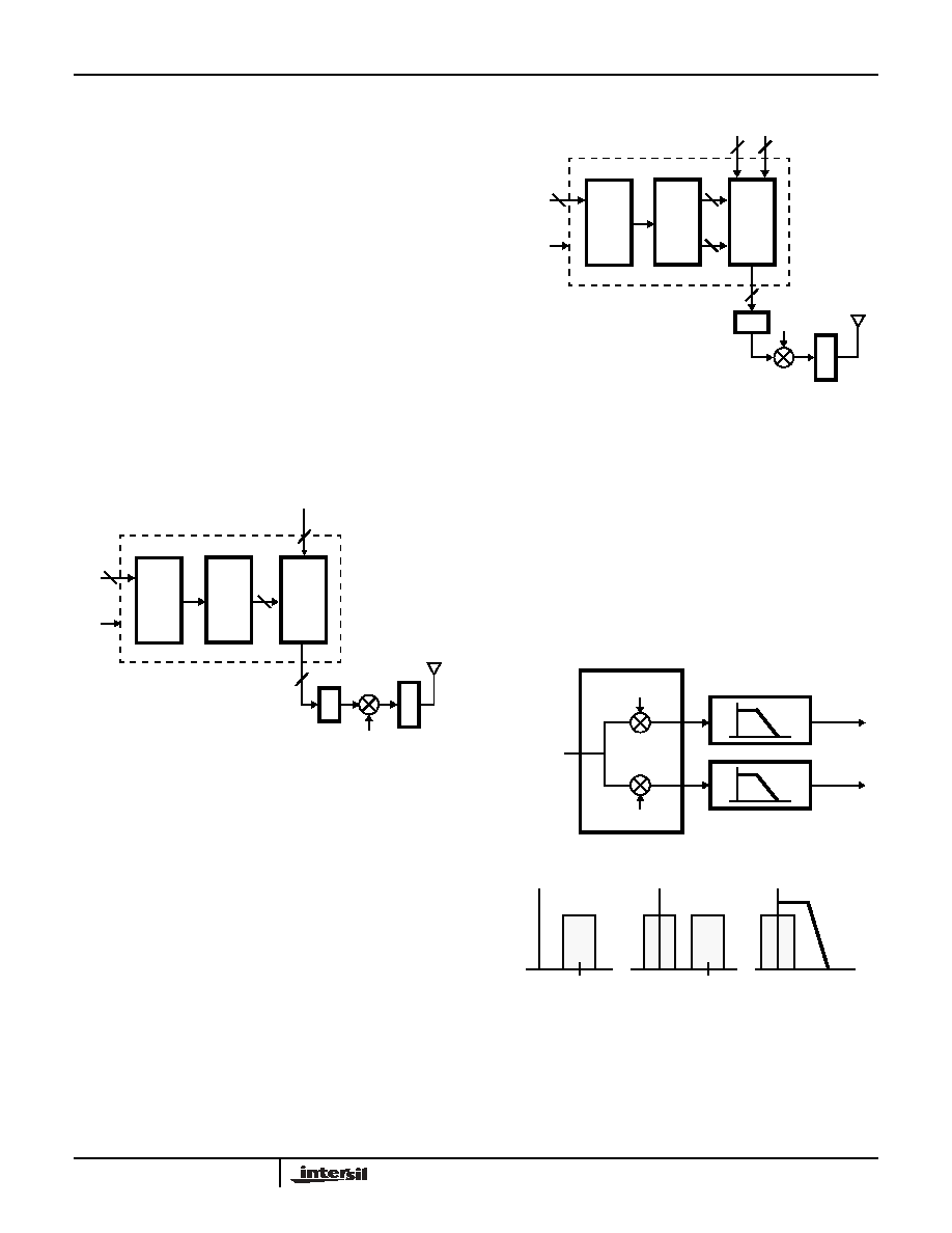
Figure 4 shows a block diagram of an AM modulator. In this
example, the phase increment for the carrier frequency is
loaded into the center frequency register, and the modulating
input is clocked into the real input of the CMAC, with the
imaginary input set to 0. The modulated output is obtained at
the real output of the CMAC. With a sixteen bit, two's
complement signal input, the output will be a 16-bit real
number, on ROUT0-15 (with OUTMUX = 00).
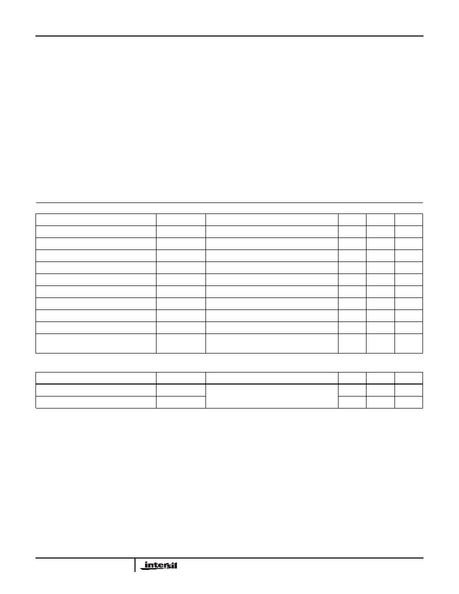
By replacing the real input with a complex vector, a similar
setup can generate QAM signals (Figure 5). In this case, the
carrier frequency is loaded into the center frequency register as
before, but the modulating vector now carries both amplitude
and phase information. Since the input vector and the internally
generated sine and cosine waves are both 16 bits, the number
of states is only limited by the characteristics of the
transmission medium and by the analog electronics in the
transmitter and receiver.
The phase and amplitude resolution for the Sine/Cosine section
(16-bit output), delivers a spectral purity of greater than 90dBc.
This means that the unwanted spectral components due to
phase uncertainty (phase noise) will be greater than 90dB
below the desired output (dBc, decibels below the carrier). With
a 32-bit phase accumulator in the Phase/Frequency Control
Section, the frequency tuning resolution equals the clock
frequency divided by 2
32
. For example, a 25MHz clock gives a
tuning resolution of 0.006Hz.
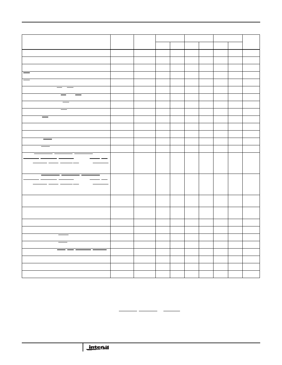
The NCOM also works with the HSP43220 Decimating
Digital Filter to implement down conversion and low pass
filtering in a digital receiver (Figure 6). The NCOM performs
complex down conversion on the wideband input signal by
multiplying the input vector and the internally generated
complex sinusoid. The resulting signal has components at
twice the center frequency and at DC. Two HSP43220s, one
each on the real and imaginary outputs of the HSP45116,
perform low pass filtering and decimation on the down
converted data, resulting in a complex baseband signal.
FIGURE 4. AMPLITUDE MODULATION
CLK
NCOM
MODULATED OUTPUT
PFCS
32
CENT
ER
F
R
EQUENCY
SIN
16
S
I
N
E
/
C
OS
INE
G
E
NERA
T
O
R
CMAC
RIN
SIGNAL INPUT
16
RO
16
D/A
XM
T
R
LO
FIGURE 5. QUADRATURE AMPLITUDE MODULATION (QAM)
CLK
NCOM
PFCS
32
CENT
ER
F
R
EQUENCY
S
I
NE
/COS
INE
GENERA
T
O
R
CMAC
RO
16
D/A
RIN
16
IMIN
16
XM
T
R
LO
16
16
FIGURE 6. CHANNELIZED RECEIVER CHIP SET
HSP43220
DDF
HSP45116
NCOM
COS (wt)
SIN (wt)
SAMPLED
INPUT
DATA
0
10MHz
DDF
OUTPUT
NCOM
OUTPUT
INPUT
0
20MHz
0
HSP45116
15
Absolute Maximum Ratings
Thermal Information
Supply Voltage . . . . . . . . . . . . . . . . . . . . . . . . . . . . . . . . . . . . . +8.0V
Input, Output or I/O Voltage Applied . . . . . GND -0.5V to V
CC
+0.5V
ESD Classification . . . . . . . . . . . . . . . . . . . . . . . . . . . . . . . . . Class 1
Operating Conditions
Operating Voltage Range. . . . . . . . . . . . . . . . . . . . +4.75V to +5.25V
Operating Temperature Range . . . . . . . . . . . . . . . . . . . 0
o
C to 70
o
C
Thermal Resistance (Typical, Note 1)
JA
(
o
C/W)
JC
(
o
C/W)
MQFP Package . . . . . . . . . . . . . . . . . .
22.0
N/A
PGA Package. . . . . . . . . . . . . . . . . . . .
23.1
3
Maximum Junction Temperature
MQFP Package . . . . . . . . . . . . . . . . . . . . . . . . . . . . . . . . . .150
o
C
PGA Package. . . . . . . . . . . . . . . . . . . . . . . . . . . . . . . . . . . . 175
o
C
Maximum Storage Temperature Range . . . . . . . . . . -65
o
C to 150
o
C
Maximum Lead Temperature (Soldering 10s) . . . . . . . . . . . . .300
o
C
(MQFP - Lead Tips Only)
Die Characteristics
Component Count . . . . . . . . . . . . . . . . . . . . . . . 103,000 Transistors
CAUTION: Stresses above those listed in "Absolute Maximum Ratings" may cause permanent damage to the device. This is a stress only rating and operation of the
device at these or any other conditions above those indicated in the operational sections of this specification is not implied.
NOTE:
1.
JA
is measured with the component mounted on an evaluation PC board in free air.
DC Electrical Specifications
PARAMETER
SYMBOL
TEST CONDITIONS
MIN
MAX
UNITS
Logical One Input Voltage
V
IH
V
CC
= 5.25V
2.0
-
V
Logical Zero Input Voltage
V
IL
V
CC
= 4.75V
-
0.8
V
High Level Clock Input
V
IHC
V
CC
= 5.25V
3.0
-
V
Low Level Clock Input
V
ILC
V
CC
= 4.75V
-
0.8
V
Output HIGH Voltage
V
OH
I
OH
= -400mA, V
CC
= 4.75V
2.6
-
V
Output LOW Voltage
V
OL
I
OL
= 2.0mA, V
CC
= 4.75V
-
0.4
V
Input Leakage Current
I
I
V
IN
= V
CC
or GND, V
CC
= 5.25V
-10
10
µ
A
I/O Leakage Current
I
O
V
OUT
= V
CC
or GND, V
CC
= 5.25V
-10
10
µ
A
Standby Power Supply Current
I
CCSB
V
IN
= V
CC
or GND V
CC
= 5.25V, Note 4
-
500
µ
A
Operating Power Supply Current
I
CCOP
f = 15MHz, V
IN
= V
CC
or GND, V
CC
= 5.25V,
Notes 2 and 4
-
182
mA
Capacitance
T
A
= 25
o
C, Note 3
PARAMETER
SYMBOL
TEST CONDITIONS
MIN
MAX
UNITS
Input Capacitance
C
IN
FREQ = 1MHz, V
CC
= Open, All measurements
are referenced to device ground
-
15
pF
Output Capacitance
C
O
-
15
pF
NOTES:
2. Power supply current is proportional to operating frequency. Typical rating for I
CCOP
is 10mA/MHz.
3. Not tested, but characterized at initial design and at major process/design changes.
4. Output load per test load circuit with switch open and C
L
= 40pF.
HSP45116
16
AC Electrical Specifications
V
CC
= 5.0V
±
5%, T
A
= 0
o
C to 70
o
C (Note 5)
PARAMETER
SYMBOL
NOTES
-15 (15MHz)
-25 (25.6MHz)
-33 (33MHz)
UNITS
MIN
MAX
MIN
MAX
MIN
MAX
CLK Period
t
CP
66
-
39
-
30
-
ns
CLK High
t
CH
26
-
15
-
12
-
ns
CLK Low
t
CL
26
-
15
-
12
-
ns
WR Low
t
WL
26
-
15
-
12
-
ns
WR High
t
WH
26
-
15
-
12
-
ns
Setup Time; AD0-1, CS to WR Going High
t
AWS
18
-
13
-
13
-
ns
Hold Time; AD0, AD1, CS from WR Going High
t
AWH
0
-
0
-
0
-
ns
Setup Time C0-15 from WR Going High
t
CWS
20
-
15
-
15
-
ns
Hold Time C0-15 from WR Going High
t
CWH
0
-
0
-
0
-
ns
Setup time WR High to CLK High
t
WC
7
20
-
16
-
12
-
ns
Setup Time MOD0-1 to CLK Going High
t
MCS
20
-
15
-
15
-
ns
Hold Time MOD0-1 from CLK Going High
t
MCH
0
-
0
-
0
-
ns
Setup Time PACI to CLK Going High
t
PCS
25
-
15
-
11
-
ns
Hold Time PACI from CLK Going High
t
PCH
0
-
0
-
0
-
ns
Setup ENPHREG, ENCFREG, ENOFREG,
ENPHAC, ENTIREG, CLROFR, PMSEL, LOAD, ENI,
ACC, BINFMT, PEAK, MODPI/2PI, SH0-1, RBYTILD
from CLK Going High
t
ECS
18
-
12
-
12
-
ns
Hold Time ENPHREG, ENCFREG, ENOFREG,
ENPHAC, ENTIREG, CLROFR, PMSEL, LOAD, ENI,
ACC, BINFMT, PEAK, MODPI/2PI, SH0-1, RBYTILD
from CLK Going High
t
ECH
0
-
0
-
0
-
ns
Setup Time RIN0-18, IMIN0-18 to CLK
Going High
t
DS
18
-
12
-
12
-
ns
Hold Time RIN0-18, IMIN0-18 from CLK
Going High
t
DH
0
-
0
-
0
-
ns
CLK to Output Delay RO0-19, IO0-19
t
DO
-
40
-
24
-
19
ns
CLK to Output Delay DET0-1
t
DEO
-
40
-
27
-
20
ns
CLK to Output Delay PACO
t
PO
-
30
-
20
-
12
ns
CLK to Output Delay TICO
t
TO
-
30
-
20
-
12
ns
Output Enable Time OER, OEI, OEREXT, OEIEXT
t
OE
-
25
-
20
-
20
ns
OUTMUX0-1 to Output Delay
t
MD
-
40
-
28
-
26
ns
Output Disable Time
t
OD
6
-
20
-
15
-
15
ns
Output Rise, Fall Time
t
RF
6
-
8
-
8
-
6
ns
NOTES:
5. AC testing is performed as follows: Input levels (CLK Input) 4.0V and 0V; input levels (all other inputs) 0V and 3.0V; timing reference levels (CLK)
2.0V; all others 1.5V. Output load per test load circuit with switch closed and C
L
= 40pF. Output transition is measured at V
OH
1.5V and V
OL
1.5V.
6. Controlled via design or process parameters and not directly tested. Characterized upon initial design and after major process and/or design
changes.
7. Applicable only when outputs are being monitored and ENCFREG, ENPHREG, or ENTIREG is active.
HSP45116
17
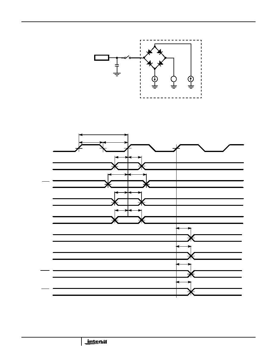
AC Test Load Circuit
Waveforms
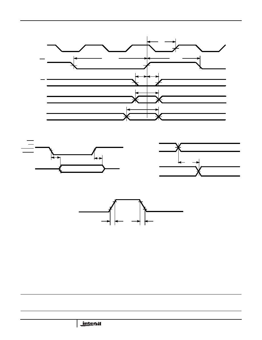
FIGURE 7. INPUT AND OUTPUT TIMING
EQUIVALENT CIRCUIT
C
L
(NOTE)
I
OH
1.5V
I
OL
DUT
SWITCH S1 OPEN FOR I
CCSB
AND I
CCOP
S
1
±
NOTE: Test head capacitance.
CLK
MOD0-1
PACI
TICO
DET0-1
PACO
ROUT0-19
IOUT0-19
CONTROL
INPUTS
t
CH
t
CP
t
PCS
t
MCS
t
ECS
t
DS
t
CL
t
MCH
t
PCH
t
ECH
t
DH
t
DO
t
DEO
t
PO
t
TO
RIN0-19
IIN0-19
HSP45116
18
All Intersil U.S. products are manufactured, assembled and tested utilizing ISO9000 quality systems.
Intersil Corporation's quality certifications can be viewed at www.intersil.com/design/quality
Intersil products are sold by description only. Intersil Corporation reserves the right to make changes in circuit design, software and/or specifications at any time without
notice. Accordingly, the reader is cautioned to verify that data sheets are current before placing orders. Information furnished by Intersil is believed to be accurate and
reliable. However, no responsibility is assumed by Intersil or its subsidiaries for its use; nor for any infringements of patents or other rights of third parties which may result
from its use. No license is granted by implication or otherwise under any patent or patent rights of Intersil or its subsidiaries.
For information regarding Intersil Corporation and its products, see www.intersil.com
FIGURE 8. CONTROL BUS TIMING
FIGURE 9. OUTPUT ENABLE, DISABLE TIMING
FIGURE 10. MULTIPLEXER TIMING
FIGURE 11. OUTPUT RISE AND FALL TIMES
Waveforms
(Continued)
t
WL
t
WC
t
WH
t
AWH
t
AWS
t
AWH
t
AWS
t
CWH
t
CWS
CLK
CS
WR
C0-15
AD0-1
HIGH
IMPEDANCE
1.5V
t
OE
1.7V
1.3V
HIGH
IMPEDANCE
1.5V
t
OD
RO0-19
IO0-19
OER
OEREXT
OEIEXT
OEI
t
MD
OUTMUX0-1
RO0-19
IO0-19
2.0V
0.8V
t
RF
t
RF
HSP45116