1
TM
HSP45256
Binary Correlator
The Intersil HSP45256 is a high-speed, 256 tap binary
correlator. It can be configured to perform one-dimensional
or two-dimensional correlations of selectable data precision
and length. Multiple HSP45256's can be cascaded for
increased correlation length. Unused taps can be masked
out for reduced correlation length.
The correlation array consists of eight 32-tap stages. These
may be cascaded internally to compare 1, 2, 4 or 8-bit input
data with a 1-bit reference. Depending on the number of bits
in the input data, the length of the correlation can be up to
256, 128, 64, or 32 taps. The HSP45256 can also be
configured as two separate correlators with window sizes
from 4 by 32 to 1 by 128 each. The mask register can be
used to prevent any subset of the 256 bits from contributing
to the correlation score.
The output of the correlation array (correlation score) feeds
the weight and sum logic, which gives added flexibility to the
data format. In addition, an offset register is provided so that
a preprogrammed value can be added to the correlation
score. This result is then passed through a user
programmable delay stage to the cascade summer. The
delay stage simplifies the cascading of multiple correlators
by compensating for the latency of previous correlators.
The Binary Correlator is configured by writing a set of control
registers via a standard microprocessor interface. To simplify
operation, both the control and reference registers are
double buffered. This allows the user to load new mask and
reference data while the current correlation is in progress.
Features
∑ Reconfigurable 256 Stage Binary Correlator
∑ 1-Bit Reference x 1, 2, 4, or 8-Bit Data
∑ Separate Control and Reference Interfaces
∑ 25.6, 33MHz Versions
∑ Configurable for 1-D and 2-D Operation
∑ Double Buffered Mask and Reference
∑ Programmable Output Delay
∑ Cascadable
∑ Standard Microprocessor Interface
Applications
∑ Radar/Sonar
∑ Spread Spectrum Communications
∑ Pattern/Character Recognition
- Error Correction Coding
Block Diagram
Ordering Information
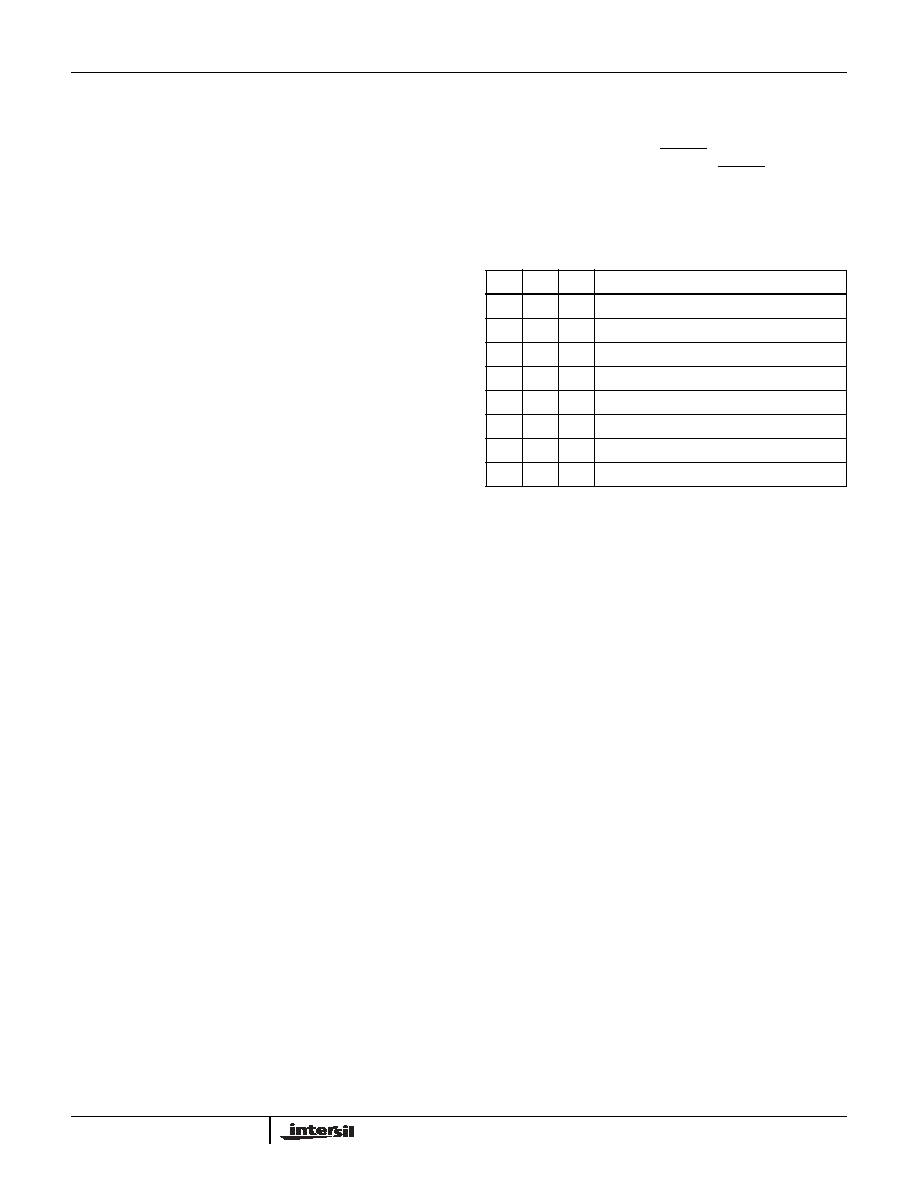
PART NUMBER
TEMP.
RANGE (
o
C)
PACKAGE
PKG.
NO.
HSP45256JC-25
0
to 70
84 Ld PLCC
N84.1.15
HSP45256JC-33
0
to 70
84 Ld PLCC
N84.1.15
HSP45256GC-25
0
to 70
85 Ld PGA
G85.A
HSP45256GC-33
0
to 70
85 Ld PGA
G85.A
HSP45256JI-25
-40 to 85
84 Ld PLCC
N84.1.15
HSP45256JI-33
-40 to 85
84 Ld PLCC
N84.1.15
256 TAP
CORRELATION
ARRAY
CONTROL
WEIGHT
AND SUM
MUX
DELAY
CASCADE
SUMMER
DIN0-7
DREF0-7
DCONT0-7
A0-2
CASIN0-12
AUXOUT0-8
CASOUT0-12
DOUT0-7
DOUT
DREFOUT
CSCORE
Data Sheet
May 1999
FN2814.4
CAUTION: These devices are sensitive to electrostatic discharge; follow proper IC Handling Procedures.
1-888-INTERSIL or 321-724-7143
|
Intersil (and design) is a trademark of Intersil Americas Inc.
Copyright © Intersil Americas Inc. 2002. All Rights Reserved
2
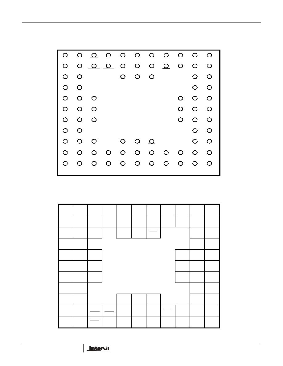
Pinouts
85 PIN PGA
BOTTOM VIEW
85 PIN PGA
TOP VIEW
A
B
C
D
E
F
G
H
J
K
L
DREF0
GND
TXFR
A2
DCONT7 DCONT1
DCONT0
DCONT3
AUX
AUX
AUX
OUT8
OUT7
OUT5
V
CC
DREF2
A0
DCONT
DCONT
RLOAD CLOAD
OEA
AUX
AUX
AUX
6
2
A1
DCONT DCONT
GND
DREF1
DREF3
5
4
AUX
OUT2
CASIN
CASIN
CASIN
CASIN
CASIN
CASIN
GND
CASOUT
8
CASOUT
5
CASOUT
CASOUT
0
2
4
5
7
10
11
CASIN6
CASIN1
CASIN
CASIN3
GND
CASOUT
10
CASOUT
CASOUT
CASOUT
4
CASOUT
1
CASOUT
2
9
DREF4
AUXOUT AUXOUT
DREF5
0
1
DIN0
DREF7
DIN1
DOUT6 DOUT5
V
CC
DIN3
DIN2
DOUT4
DREF6
DOUT7 DOUT3
DOUT0 DOUT1 DOUT2
DIN4
DIN6
DIN5
GND
DIN7
CASOUT
12
V
CC
CLK
CASIN0
CASIN
CASIN
OEC
CASOUT
11
CASOUT
INDEX
PIN
8
12
OUT6
OUT4
OUT3
9
7
1
2
3
4
5
6
7
8
9
10
11
3
A
B
C
D
E
F
G
H
J
K
L
2
1
7
3
4
5
6
8
9
10
11
CLK
DIN7
DIN4
DIN0
DREF
DREF
DREF
GND
DREF
CASIN
2
0
2
5
6
DREF
3
V
CC
CASIN
CASIN
DIN3
DREF
DREF
V
CC
GND
DIN5
CASIN
4
1
0
1
4
DREF
7
INDEX
PIN
DIN6
DIN2
DIN1
TXFR
CASIN
R
CASIN
5
LOAD
3
A2
C
CASIN
CASIN
7
6
LOAD
CASIN
A1
A0
DCONT
CASIN
CASIN
10
9
8
7
DCONT
DCONT
DCONT
CASIN
CAS
CASIN
12
11
1
6
5
OUT2
OEC
DCONT
DCONT
DCONT
CAS
CAS
3
2
4
OUT
OUT1
DCONT
CAS
OEA
CAS
0
OUT3
OUT4
DOUT0
DOUT
V
CC
CAS
AUX
CAS
4
OUT5
OUT6
AUX
OUT6
OUT8
GND
DOUT
DOUT
GND
DOUT
CAS
CAS
AUX
AUX
AUX
GND
7
6
OUT7
OUT9
OUT1
OUT4
OUT7
DOUT2
DOUT
DOUT
CAS
CAS
CAS
AUX
AUX
AUX
AUX
CAS
3
5
OUT8
OUT10
OUT11
OUT12
OUT0
OUT2
OUT3
OUT5
HSP45256
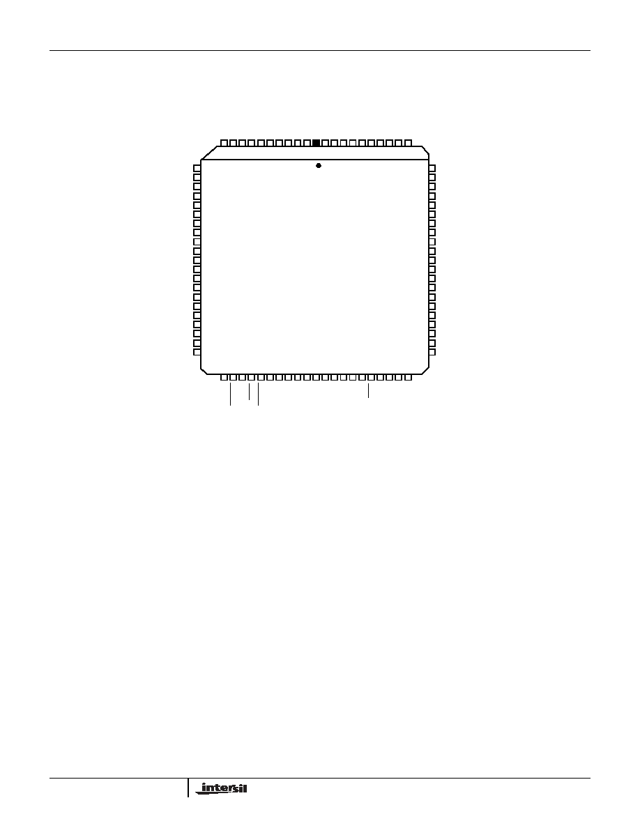
3
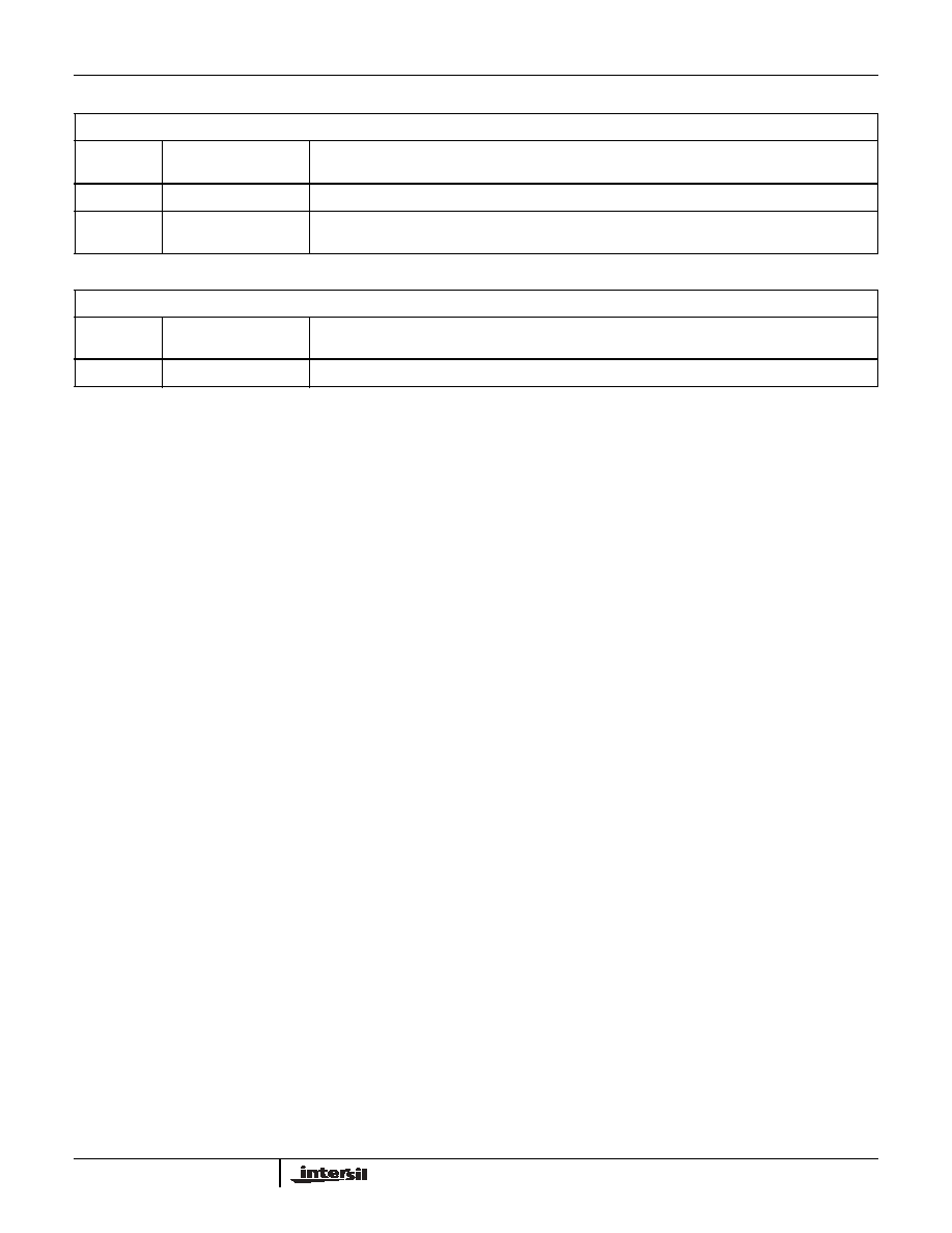
84 PIN PLCC
TOP VIEW
Pinouts
(Continued)
11 10 9 8 7 6 5 4 3 2 1 84 83 82 81 80 79 78 77 76 75
12
13
14
15
16
17
18
19
20
21
22
23
24
25
26
27
28
29
30
31
32
33 34 35 36 37 38 39 40 41 42 43 44 45 46 47 48 49 50 51 52 53
74
73
72
71
70
69
68
67
66
65
64
63
62
61
60
59
58
57
56
55
54
V
CC
RL
O
A
D
GN
D
TX
FR
CL
O
A
D
A2
A1
A0
DCO
NT
7
DCO
NT
6
DCO
NT
5
DCO
NT
4
DCO
NT
3
DCO
NT
2
DCO
NT
1
DCO
NT
0
OE
A
AUX
O
U
T
8
AUX
O
U
T
7
AUX
O
U
T
5
AUX
O
U
T
6
CASIN1
CASIN0
GND
CLK
V
CC
DIN7
DIN6
DIN5
DIN4
DIN3
DIN2
DIN1
DIN0
DREF7
DREF6
DREF5
DREF4
DREF3
DREF2
DREF1
DREF0
CASOUT8
CASOUT9
CASOUT10
CASOUT11
GND
CASOUT12
DOUT0
DOUT1
DOUT2
DOUT3
DOUT4
V
CC
DOUT5
DOUT6
DOUT7
AUXOUT0
AUXOUT1
AUXOUT2
AUXOUT3
GND
AUXOUT4
CA
S
I
N
2
CA
S
I
N
3
CA
S
I
N
4
CA
S
I
N
5
CA
S
I
N
6
CA
S
I
N
7
CA
S
I
N
8
CA
S
I
N
9
CA
S
I
N
1
0
CA
S
I
N
1
1
CA
S
I
N
1
2
OE
C
#
CA
S
O
U
T
0
CA
S
O
U
T
1
CA
S
O
U
T
2
CA
S
O
U
T
3
CA
S
O
U
T
4
CA
S
O
U
T
5
GN
D
CA
S
O
U
T
7
CA
S
O
U
T
6
HSP45256
4
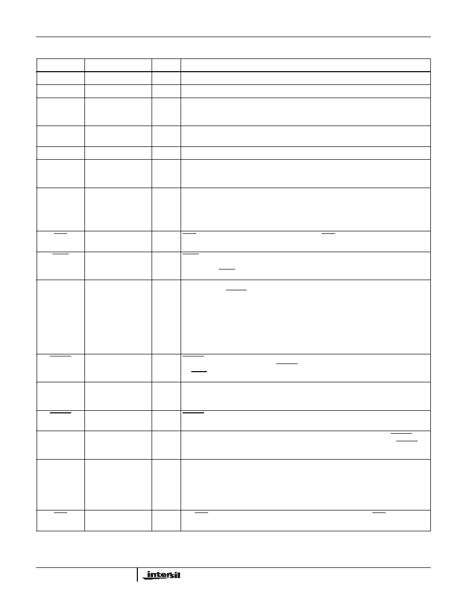
Pin Descriptions
SYMBOL
PLCC PIN NUMBER
TYPE
DESCRIPTION
V
CC
16, 33, 63
The +5V power supply pin.
GND
14, 35, 55, 70, 77
Ground.
DIN0-7
17-24
I
The DIN0-7 bus consists of eight single data input pins. The assignment of the active pins is
determined by the configuration. Data is loaded synchronous to the rising edge of CLK. DIN0
is the LSB.
DOUT0-7
60-62, 64-68
O
The DOUT0-7 bus is the data output of the correlation array. The format of the output is de-
pendent on the window configuration and bit weighting. DOUT0 is the LSB.
CLK
15
I
System Clock. Positive edge triggered.
CASIN0-12
1-13
I
CASIN0-12 allows multiple correlators to be cascaded by connecting CASOUT0-12 of one
correlator to CASIN0-12 of another. The CASIN bus is added internally to the correlation
score to form CASOUT. CASIN0 is the LSB.
CASOUT0-12
69, 71-76, 78-83
O
CASOUT0-12 is the output correlation score. This value is the delayed sum of all the 256
taps of one chip and CASIN0-12. When the part is configured to act as two independent cor-
relators, CASOUT0-8 represents the correlation score for the first correlator while the sec-
ond correlation score is available on the AUXOUT0-8 bus. In this configuration, the
cascading feature is no longer an option. CASOUT0 is the LSB.
OEC
84
I
OEC is the output enable for CASOUT0-12. When OEC is high, the output is three-stated.
Processing is not interrupted by this pin (active low).
TXFR
36
I
TXFR is a synchronous clock enable signal that allows the loading of the reference and mask
inputs from the preload register to the correlation array. Data is transferred on the rising edge
of CLK while TXFR is low (active low).
DREF0-7
25-32
I
DREF0-7 is an 8-bit wide data reference input. This is the input data bus used to load the
reference data. RLOAD going active initiates the loading of the reference registers. This in-
put bus is used to load the reference registers of the correlation array. The manner in which
the reference data is loaded is determined by the window configuration. If the window con-
figuration is 1 x 256, the reference bits are loaded one at a time over DREF7. When the
HSP45256 is configured as an 8 x 32 array, the data is loaded into all stages in parallel. In
this case, DREF7 is the reference data for the first stage and DREF0 is the reference data
for the eighth stage. The contents of the reference data registers are not affected by chang-
ing the window configuration. DREF0 is the LSB.
RLOAD
34
I
RLOAD enables loading of the reference registers. Data on DREF0-7 is loaded into the pre-
load registers on the rising edge of RLOAD. This data is transferred into the correlation array
by TXFR (active low).
DCONT0-7
41-48
I
DCONT0-7 is the control data input which is used to load the mask bit for each tap, as well
as the configuration registers. The mask data is sequentially loaded into the eight stages in
the same manner as the reference data. DCONT0 is the LSB.
CLOAD
37
I
CLOAD enables the loading of the data on DCONT0-7. The destination of this data is con-
trolled by A0-2 (active low).
A0-2
38-40
I
A0-2 is a 3-bit address that determines what function will be performed when CLOAD is ac-
tive. This address bus is set up with respect to the rising edge of the load signal, CLOAD. A0
is the LSB.
AUXOUT0-8
50-54, 56-59
O
AUXOUT0-8 is a 9-bit bus that provides either the data reference output in the single corre-
lation configuration or the 9-bit correlation score of the second correlator, in the dual corre-
lator configuration. When the user programs the chip to be two separate correlators, the
score of the second correlator is output on this bus. When the user has programmed the chip
to be one correlator, AUXOUT0-7 represents the reference data out, with the state of
AUXOUT8 undefined. AUXOUT0 is the LSB.
OEA
49
I
The OEA signal is the output enable for the AUXOUT0-8 output. When OEA is high, the out-
put is disabled. Processing is not interrupted by this pin (active low).
HSP45256
5
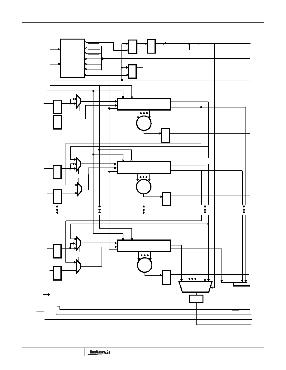
Block Diagram
NOTE: All registers clocked with CLK unless otherwise specified.
CORRELATOR BLOCK DIAGRAM
MASK
CONFIG
OFFAL
OFFAM
DELAY
OFFBL
OFFBM
DECODE
CLOAD
A(2:0)
32 TAP CORRELATOR STAGE
RLOAD
TXFR
DIN7
DREF7
DO7
RO7
MUX
ARRAY
+
CO7
CORRELATION
SCORE OUT
DIN6
DREF6
DO6
RO6
CO6
32 TAP CORRELATOR STAGE
DO0
RO0
CO0
RO7
DIN0
DREF0
RO1
MR7
MR6
MR0
DATA OUT
DO7
DO1
R
E
G
>
R
E
G
>
R
E
G
>
R
E
G
>
R
E
G
>
32 TAP CORRELATOR STAGE
+
R
E
G
>
R
E
G
>
+
R
E
G
>
R
E
G
>
R
E
G
>
R
E
G
>
R
E
G
>
DCONT(7:0)
RO7
RO6
RO0
REFERENCE OUT
CASIN(12:0)
DOUT(7:0)
OEA
OEC
CASIN(12:0)
OEA
OEC
(000)
(001)
8
6
CONFIG(4:0)
TC
TC
5
CONFIG(4:0)
CONFIG(4:0)
CLK
DATA OUT
R
E
G
>
HSP45256
6
NOTE:
All registers clocked with CLK
unless otherwise specified.
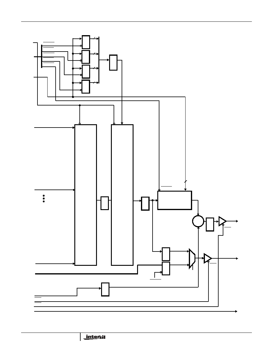
Block Diagram
(Continued)
WEIGHT
SUM
OFFSET
REGISTER A
PROGRAMMABLE
DELAY
OFFSET
REGISTER B
AUXOUT(8:0)
CASCADE
REGISTER
+
CASIN(12:0)
RO(0-7)
OEA
OEC
CASOUT(12:0)
RLOAD
OFFAL
OFFAM
DELAY
OFFBL
OFFBM
R
E
G
>
R
E
G
>
DELAY
R
E
G
>
R
E
G
>
R
E
G
>
CO7
CO6
CO0
CORRELATION
SCORE OUT
REFERENCE OUT
R
E
G
>
R
E
G
>
R
E
G
>
R
E
G
>
R
E
G
>
R
E
G
>
DOUT(7:0)
DOUT(7:0)
OEA
OEC
(100)
4
(010)
(011)
(101)
(110)
5
8
1
8
CONFIG(4:0)
CONFIG(4:0)
HSP45256
7
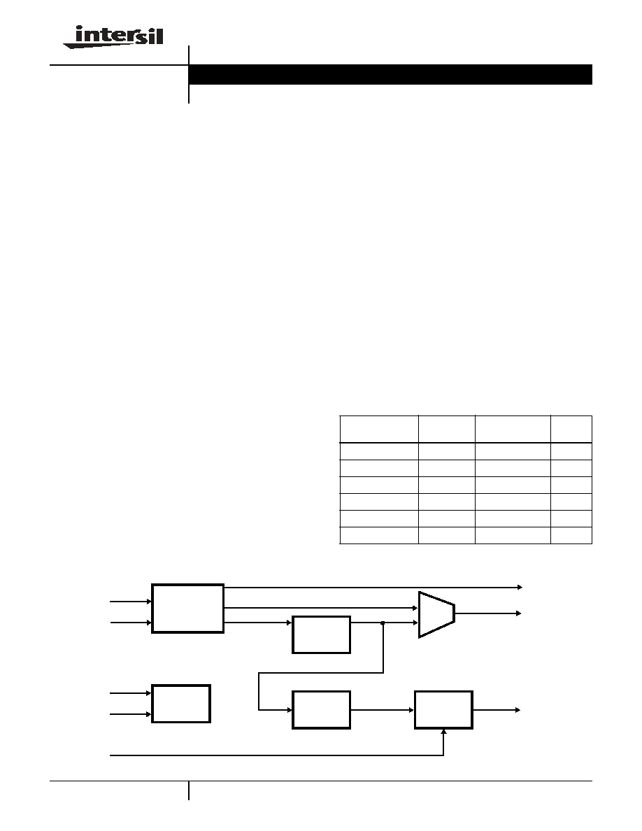
Functional Description
The correlation array consists of eight 32-bit stages. The first
stage receives data directly from input pin DIN7. The other
seven stages receive input data from either an external data
pin, DIN0-6, or from the Shift Register output of the previous
stage, as determined by the Configuration Register. When
the part is configured as a single correlator the sum of
correlation score, Offset Register and cascade input
appears on CASOUT0-12. Delayed versions of the data and
reference inputs appear on DOUT0-7 and AUXOUT0-7,
respectively. The input and output multiplexers of the
correlation array are controlled together; for example, in a 1
x 256 correlation, the input data is loaded into DIN7 and the
output appears on DOUT7. The configuration of the data
bits, the length of the correlation (and in the two-dimensional
data, the number of rows), is commonly called the
correlation window. A top level Block Diagram of the single
correlator configuration is shown in Figure 1. Compare the
single correlator configuration data output and correlation
output to the top level Block Diagram of the dual correlator
configuration shown in Figure 2.
Correlator Array
The core of the HSP45256 is the correlation array, which
consists of eight 32-tap stages. A single correlator cell
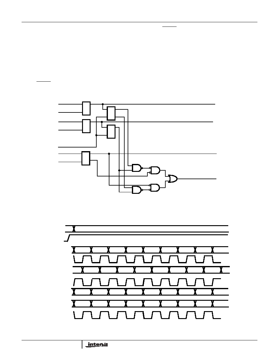
consists of an XNOR gate for the individual bit comparison;
i.e., if the data and reference bits are either both high or both
low, the output of the correlator cell is high. Figure 3 details
the circuitry of a single correlation cell and Figure 4 shows
the timing for that single correlation cell. In addition, two
latches, one for the reference and one for the control data
path are contained in this cell. These latches are loaded
from the Preload Registers on the rising edge of CLK when
TXFR is low so that the reference and mask values are
updated without interrupting data processing.
The mask function is implemented with an AND gate. When
a mask bit is a logic low, the corresponding correlator cell
output is low.
8 32-BIT
CORRELATORS
DIN(7:0)
DREF(7:0)
DOUT(7:0)
SUM
WEIGHT
AND
CORR
SCORE
SUM
DELAY
SUM
OFFA
CASIN(12:0)
CASOUT(12:0)
AUXOUT(7:0)
FIGURE 1. SINGLE CORRELATOR CONFIGURATION
∑ ∑ ∑ ∑ ∑ ∑ ∑ ∑ ∑ ∑ ∑ ∑
FIGURE 2. DUAL CORRELATOR CONFIGURATION
∑ ∑ ∑ ∑ ∑ ∑ ∑ ∑ ∑ ∑ ∑ ∑
∑ ∑ ∑ ∑ ∑ ∑ ∑ ∑ ∑ ∑ ∑ ∑
4 32-BIT
CORRELATORS
DIN(7:4)
DREF(7:4)
DOUT(7:4)
SUM
WEIGHT
AND
CORR
SCORE
SUM
DELAY
SUM
OFFA
CASOUT(8:0)
= 0000
CASIN(12:0)
4 32-BIT
CORRELATOR
DIN(3:0)
DOUT (3:0)
DREF(3:0)
SUM
CORR
SCORE
WEIGHT
AND
SUM
OFFB
AUXOUT(8:0)
CORRELATOR #1
CORRELATOR #2
HSP45256
8
The function performed by one correlation cell is:
(D
i,n
XNOR R
i,n
) AND M
i,n
where:
D
i,n
= Bit i of data register n
R
i,n
= Bit i of reference register n
M
i,n
= Bit i of mask register n
The reference and mask bits are loaded sequentially, N bits
at a time, where N depends on the current configuration (see
Tables 2 and 9). New reference data is loaded on the rising
edge of RLOAD and new mask data is loaded on the rising
edge of CLOAD. The mask and reference bits are stored
internally in Shift Registers, so that the mask and reference
information that was loaded most recently will be used to
process the newest data. When new information is loaded
in, the previous contents of the mask and reference bits are
shifted over by one sample, and the oldest information is
lost. There are no registers in the multiplexer array (see
Block Diagram), so the data on DOUT0-7 corresponds to the
data in the last element of the correlation array. When
monitoring DOUT0-7, AUXOUT0-8, and REFOUT0-7, only
those bits listed in Table 9 are valid.
FIGURE 3. CORRELATION CELL BLOCK DIAGRAM
FIGURE 4. CORRELATION CELL TIMING DIAGRAM
R
E
G
>
RLOAD
DREF
R
E
G
>
DCONT
CLOAD
DREFOUT
DCONTOUT
R
E
G
>
TXFR
R
E
G
>
CLK
DATA
DATAOUT
COROUT
A
B
R
E
G
>
(MASK)
RLOAD
DREF
DCONT
CLOAD
TXFR
CLK
DATA
DATA CONTROL
A
B
DR8
DR7
DR6
DR5
DR4
DR3
DR2
DR1
DR0
DR7
DR6
DR5
DR4
DR3
DR2
DR1
DR0
DR7
DR6
DR5
DR4
DR3
DR2
DR1
DR0
DR-1
D7
D6
D5
D4
D3
D2
D1
D0
D-1
HSP45256
9
Weight and Sum Logic
The Weight and Sum Logic provides the bit weighting and
the final correlator score from the eight stages of the
correlation array. For a 1 x 256 1-D configuration, the
outputs of each of the stages are given a weight of 1 and
then added together. In a 8 x 32 (8-bit data) configuration,
the output of each stage will be shifted so that the output
data represents an 8-bit word, with stage seven being the
MSB.
The 13-bit Offset Register is loaded from the control data
bus. Its output is added to the correlation score obtained
from the correlator array. This sum then goes to the
programmable delay register data input.
When the chip is configured as dual correlators, the user has
the capability of loading two different offset values, one for
each of the two correlators.
The Programmable Delay Register sets the number of
pipeline stages between the output of the weight and sum
logic and the input of the Cascade Summer. This delay
register is used to align the correlation scores of multiple
correlators in HSP45256 cascaded configurations (see
Applications Section). The number of delays is
programmable from 1 to 16, allowing for up to 16 correlators
to be cascaded. When the HSP45256 is configured as dual
correlators, the delay must be set to 0000, which specifies a
delay of 1.
Cascade Summer
The Cascade Summer is used for cascading several
correlator chips together. The value present on this bus
represents the correlation score from the previous
HSP45256 that will be summed with the current score to
provide the final correlation score. When several correlator
chips are cascaded, the CASOUT0-12 of each correlator is
connected to the CASIN0-12 of the next correlator in the
chain. The CASIN0-12 of the first chip is tied low. The
following function represents the correlation score present
on CASOUT0-12 of each correlator:
CASOUT(n) = (W7 x CO7)(n-Delay) + (W6 x CO6)(n-Delay) +
(W5 x CO5)(n-Delay) + (W4 x CO4)(n-Delay) +
(W3 x CO3)(n-Delay) + (W2 x CO2)(n-Delay) +
(W1 x CO1)(n-Delay) + (W0 x CO0)(n-Delay) +
Offset (n-Delay) + CASIN.
where:
CO0-CO7 are the correlation score outputs out of the
correlation stages; W0-W7 is the weight given to each stage;
n-Delay represents the delay on the weighted and summed
correlation score through the Programmable Delay Register;
Offset is the value programmed into the Offset register;
CASIN is the cascade input.
Control Registers
The 3-bit address value, A0-2, is used to determine which
internal register will be loaded with the data on DCONT0-7.
The function is initiated when CLOAD is brought low, and the
register is loaded on the rising edge of CLOAD. Table 1
indicates the function associated with each address. Tables
2 - 8 define the function of the bits in each of the control
registers.
TABLE 1. ADDRESS MAPPING
A2
A1
A0
DESTINATION
0
0
0
Mask Register
0
0
1
Configuration Register
0
1
0
Offset Register A-Most Significant Bits
0
1
1
Offset Register A-Least Significant Bits
1
0
0
Programmable Delay Register
1
0
1
Offset Register B-Most Significant Bits
1
1
0
Offset Register B-Least Significant Bits
1
1
1
Reserved
HSP45256
10
TABLE 2. MASK REGISTER
DESTINATION ADDRESS = 0 (000)
BIT
POSITIONS
FUNCTION
DESCRIPTION
7-0
Mask Register
Bit Enable
MR(7:0): Mask Register. When mask register bit N = 1, the corresponding reference register bit is en-
abled. Mask register data is loaded from the DCONT(7:0) bus into a holding register on the rising edge
of CLOAD and is written to the mask register on the rising edge of TXFR.
TABLE 3. CONFIGURATION REGISTER
DESTINATION ADDRESS = 1 (001)
BIT
POSITION
FUNCTION
DESCRIPTION
7-6
Reserved
Reserved; Program to zero.
5
TC
Configures correlator for twos complement input format, where the position of the MSB is depends on
the current configuration. TC = 1 is twos complement; TC = 0 is offset binary.
4
CONFIG(4)
CONFIG4: The state of CONFIG4 configures the HSP45256 as either one or two correlators. When
CONFIG4 = 0, the HSP45256 is configured as one correlator with the correlation score available on
CASOUT0-12.
When CONFIG4 = 1, the HSP45256 is configured as dual correlators with the first correlators score
available on CASOUT0-8 and the second score available on AUXOUT0-8. When the chip is configured
as dual correlators, the Programmable Delay must be set to 0000 for a delay of 1.
3-2
CONFIG(3:2):
CONFIG(3:2): Control the number of data bits to be correlated. See Table 9.
1-0
CONFIG(1:0)
CONFIG(1:0): CONFIG1 and CONFIG0 represent the length of the correlation window as indicated in
Table 9.
TABLE 4. MS OFFSET REGISTER A
DESTINATION ADDRESS = 2 (010)
BIT
POSITION
FUNCTION
DESCRIPTION
7-5
Reserved
Reserved. Program to zero.
4-0
Offset Register A MSB
OFFA(12:8): Most significant bits of Offset Register A. This is the register used in single correlator
mode.
TABLE 5. LS OFFSET REGISTER A
DESTINATION ADDRESS = 3 (011)
BIT
POSITION
FUNCTION
DESCRIPTION
7-0
Offset Register A LSB
OFFA(7:0): Least significant bits of Offset Register A.
TABLE 6. PROGRAMMABLE DELAY REGISTER
DESTINATION ADDRESS = 4 (100)
BIT
POSITION
FUNCTION
DESCRIPTION
7-4
Reserved
Reserved. Program to zero.
3-0
Programmable Delay
PDELAY(3:0): Controls amount of delay from the weight and sum logic to the cascade summer. The
number of delays is 1-16, with PDELAY = 0000 corresponding to a delay of 1 and PDELAY = 1111 cor-
responding to a delay of 16.
HSP45256
11
TABLE 7. MS OFFSET REGISTER B
DESTINATION ADDRESS = 5 (101)
BIT
POSITION
FUNCTION
DESCRIPTION
7-1
Reserved
Reserved. Program to zero.
0
Offset Register B MSB
OFFB8: Most significant bit of Offset Register B. In dual correlator mode, this register is used for the
correlator whose output appears on the AUXOUT pins.
TABLE 8. LS OFFSET REGISTER B
DESTINATION ADDRESS = 6 (110)
BIT
POSITION
FUNCTION
DESCRIPTION
7-0
Offset Register B LSB
OFFB0-7: Least significant bits of Offset Register B.
HSP45256
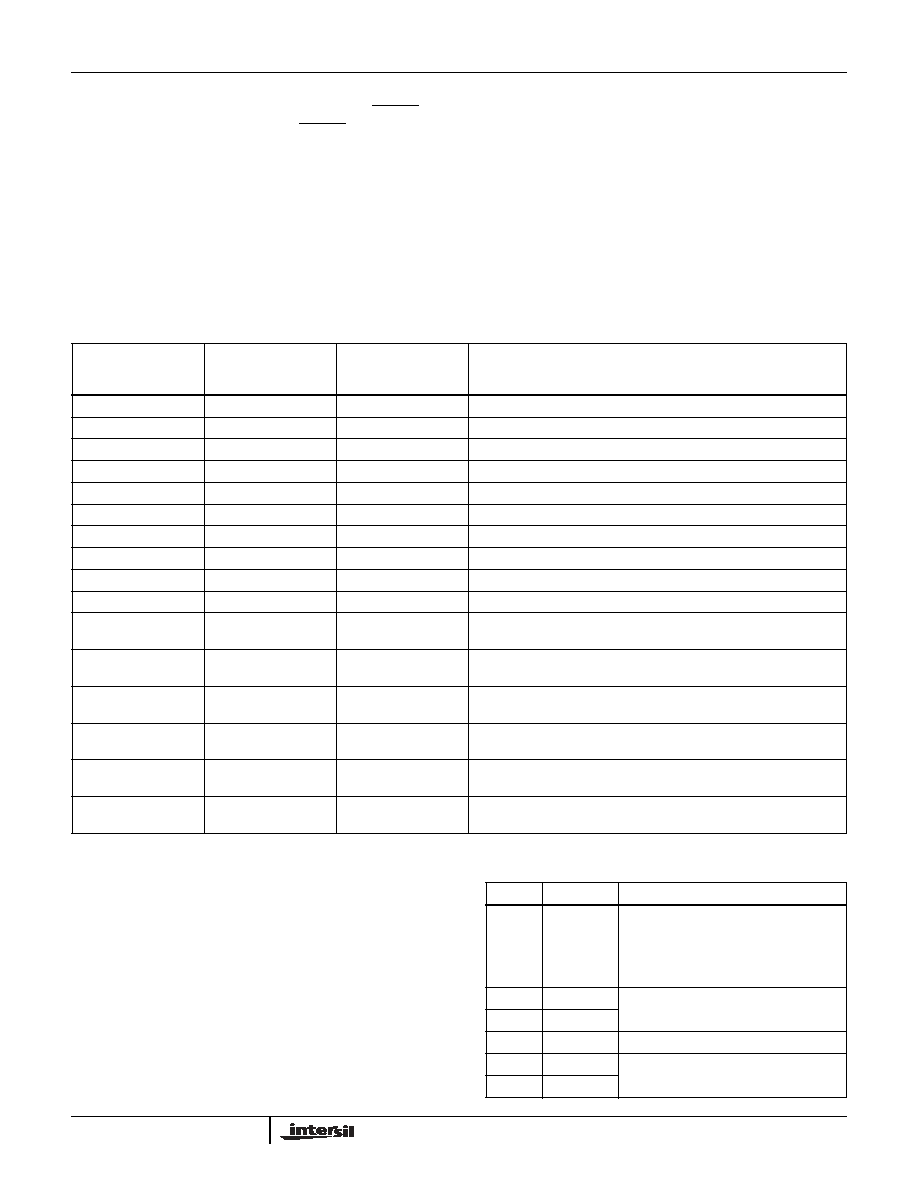
12
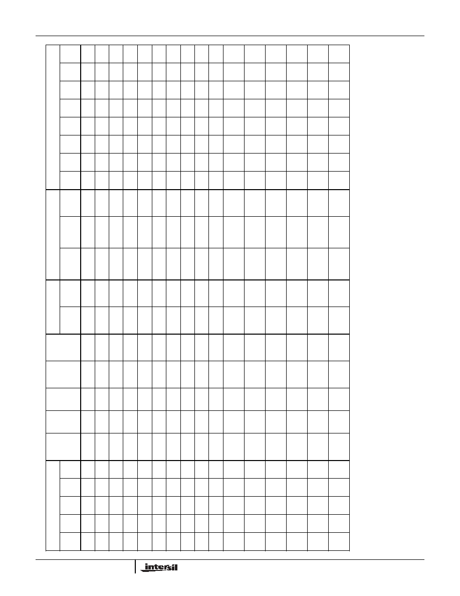
TABLE 9. CONFIGURATION SETUP
CONFIGURATION
NO.
OF
CORRE-
LATORS
DATA
BITS
ROWS LENGTH
CORRE-
LATOR
ACTIVE INPUTS
ACTIVE OUTPUTS
OUTPUT WEIGHTING
4
3
2
1
0
DIN
DREF
DOUT
AUXOUT
CASOUT CO7
CO6
CO5
CO4
CO3
CO2
CO1
CO0
0
0
0
0
0
1
1
1
256
-
7
7
7
7
12-0
1
1
1
1
1
1
1
1
0
0
0
0
1
1
1
2
128
-
7, 3
7, 3
7, 3
7, 3
12-0
1
1
1
1
1
1
1
1
0
0
0
1
0
1
1
4
64
-
7, 5, 3, 1
7, 5, 3, 1
7, 5, 3, 1
7, 5, 3, 1
12-0
1
1
1
1
1
1
1
1
0
0
0
1
1
1
1
8
32
-
7-0
7-0
7-0
7-0
12-0
1
1
1
1
1
1
1
1
0
0
1
0
1
1
2
1
128
-
7, 3
7
7, 3
7, 3
12-0
2
2
2
2
1
1
1
1
0
0
1
1
0
1
2
2
64
-
7, 5, 3, 1
7, 5
7, 5, 3, 1
7, 5, 3, 1
12-0
2
2
2
2
1
1
1
1
0
0
1
1
1
1
2
4
32
-
7-0
7, 6, 5, 4
7-0
7-0
12-0
2
2
2
2
1
1
1
1
0
1
0
1
0
1
4
1
64
-
7, 5, 3, 1
7
7, 5, 3, 1
7, 5, 3, 1
12-0
8
8
2
2
4
4
1
1
0
1
0
1
1
1
4
2
32
-
7-0
7, 6
7-0
7-0
12-0
8
8
2
2
4
4
1
1
0
1
1
1
1
1
8
1
32
-
7-0
7
7-0
7-0
12-0
128
8
32
4
64
2
16
1
1
0
0
0
1
2
1
1
128
A
B
7
3
7
3
7
3
-
8-0
12-0
-
1
-
1
-
1
-
1
-
-
1
-
1
-
1
-
1
1
0
0
1
0
2
1
2
64
A
B
7, 5
3, 1
7, 5
3, 1
7, 5
3, 1
-
8-0
12-0
-
1
-
1
-
1
-
1
-
-
1
-
1
-
1
-
1
1
0
0
1
1
2
1
4
32
A
B
7-4
3-0
7-4
3-0
7-4
3-0
-
8-0
12-0
-
1
-
1
-
1
-
1
-
-
1
-
1
-
1
-
1
1
0
1
1
0
2
2
1
64
A
B
7, 5
3, 1
7
3
7, 5
3, 1
-
8-0
12-0
-
2
-
2
-
1
-
1
-
-
2
-
2
-
1
-
1
1
0
1
1
1
2
2
2
32
A
B
7-4
3-0
7, 6
3, 2
7-4
3-0
-
8-0
12-0
-
2
-
2
-
1
-
1
-
-
2
-
2
-
1
-
1
1
1
0
1
1
2
4
1
32
A
B
7-4
3-0
7
3
7-4
3-0
-
8-0
12-0
-
8
-
2
-
4
-
1
-
-
8
-
2
-
4
-
1
H
S
P
4
5
256
13
During reference register loading, the 8-bits, DREF0-7 are
used as reference data inputs. The falling edge of RLOAD
initiates reference data loading; when RLOAD returns high,
the data on DREF0-7 is latched into the selected correlation
stages. The active bits on DREF0-7 are determined by the
current configuration.
The window configuration is determined by the state of control
signals upon programming the Control Register. Table 9
represents the programming information required for each
window configuration. In Table 9, note that the data listed for
Output Weighting refers to the weights given to each of the
Correlation Sum Outputs (CO0-7 in the Block Diagram).
During initialization, the loading configuration for the
reference data is set by the user. Table 9 shows the loading
options. These load controls specify whether the reference
data for a given stage comes from the shift register output of
the previous stage or from an external data pin.
Applications
There are 10 single correlator configurations possible with
the HSP45256. There are six dual correlator configurations
possible with the HSP45256. Table 10 details the
configuration (bits x rows x length) and the maximum
correlation sums of all combinations.
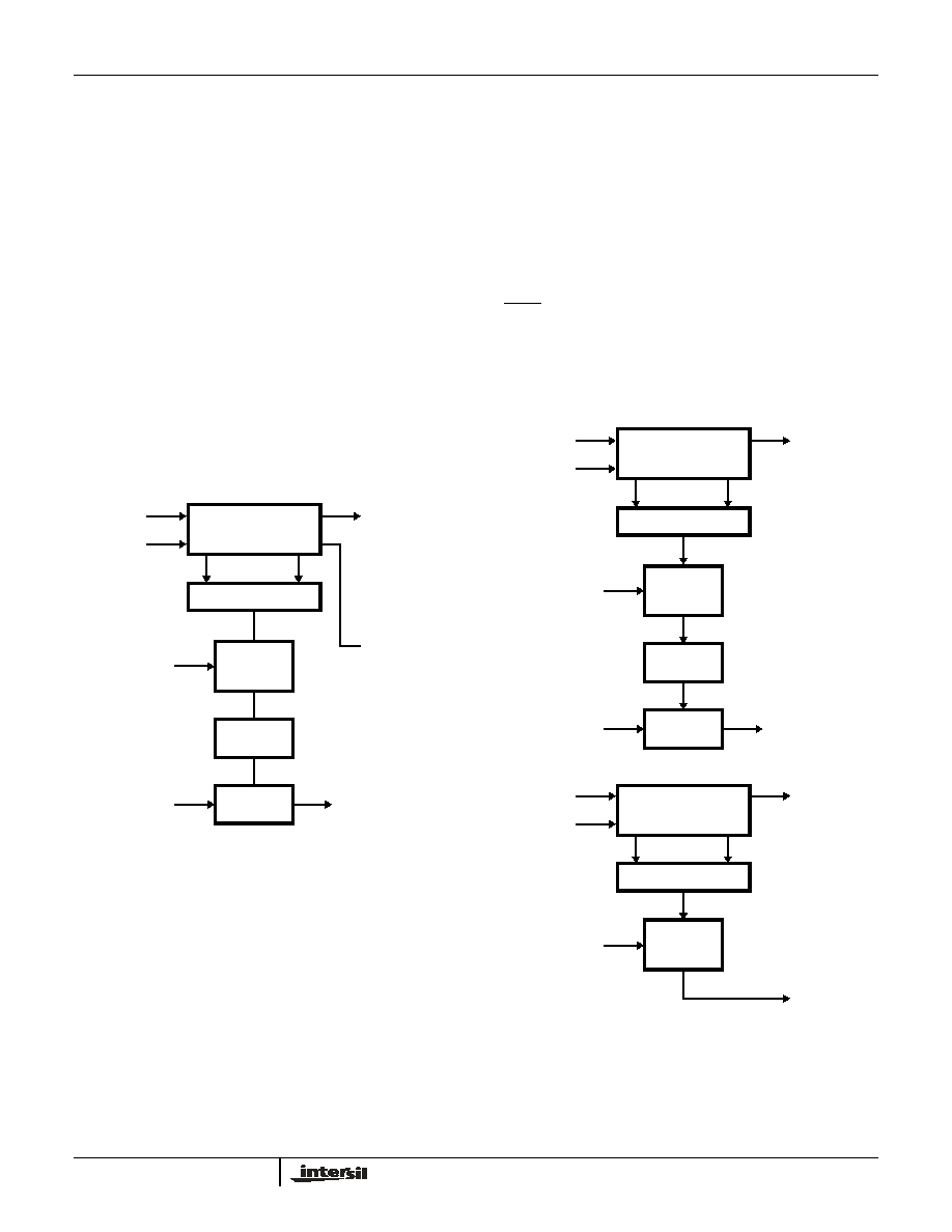
Single Correlator Configurations
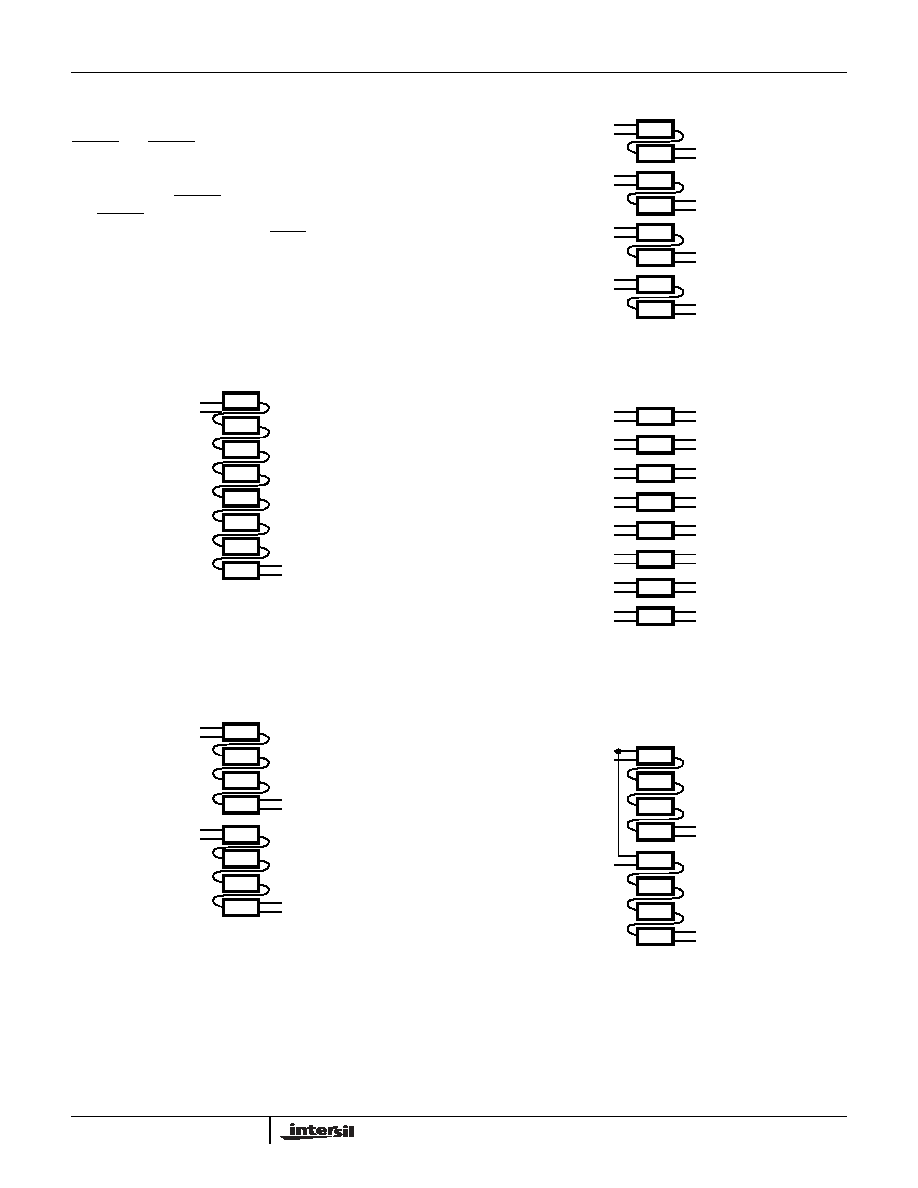
1-Bit Data, Single Row, 256 Samples Configuration
A 1 x 256 (1-D configuration) correlation requires only 1
HSP45256. To initialize the correlator, all the reference bits,
control bits, the delay value of the variable delay, and the
window configuration must be specified. Table 11 details
these settings for the 1-bit data, 256 Samples Configuration.
Figure 5 illustrates the data flow through the correlator.
TABLE 10. CORRELATION SCORE FORMULAS FOR SINGLE CORRELATOR CONFIGURATIONS
FIGURE NUMBER
CONFIGURATION
BITS x ROWS x
LENGTH
HIGHEST POSSIBLE
TOTAL CORRELA-
TION SCORE
CORRELATION SCORE
Figure 5
1 x 1 x 256
256
CS=CO7+CO6+CO5+CO4+CO3+CO2+CO1+CO0
Figure 6
1 x 2 x 128
256
CS=CO7+CO6+CO5+CO4+CO3+CO2+CO1+CO0
Figure 7
1 x 4 x 64
256
CS=CO7+CO6+CO5+CO4+CO3+CO2+CO1+CO0
Figure 8
1 x 8 x 32
256
CS=CO7+CO6+CO5+CO4+CO3+CO2+CO1+CO0
Figure 9
2 x 1 x 128
384
CS=2(CO7+CO6+CO5+CO4)+CO3+ CO2+CO1+CO0
Figure 10
2 x 2 x 64
384
CS=2(CO7+CO6+CO5+CO4)+CO3+CO2+CO1+CO0
Figure 11
2 x 4 x 32
384
CS=2(CO7+CO6+CO5+CO4)+CO3+CO2+CO1+CO0
Figure 12
4 x 1 x 64
960
CS=8(CO7+CO6)+4(CO5+CO4)+2(CO3+CO2)+CO1+CO0
Figure 13
4 x 2 x 32
960
CS=8(CO7+CO6)+4(CO5+CO4)+2(CO3+CO2)+CO1+CO0
Figure 14
8 x 1 x 32
8160
CS=128C07+64CO6+32C05+16CO4+8CO3+4CO2+2CO1+CO0
Figure 15
1 x 1 x 128
1 x 1 x 128
128
CS=CO7+CO6+CO5+CO4CS=CO31CO2+CO1+CO0
Figure 16
1 x 2 x 64
1 x 2 x 64
128
CS=CO7+CO6+CO5+CO4CS=CO31CO2+CO1+CO0
Figure 17
1 x 4 x 32
1 x 4 x 32
128
CS=CO7+CO6+CO5+CORCS=CO31CO2+CO1+CO0
Figure 18
2 x 1 x 64
2 x 1 x 64
192
CS=2(CO7+CO6)+CO5+CO4CS=(CO3+CO2)+CO1+CO0
Figure 19
2 x 2 x 32
2 x 2 x 32
192
CS=2(CO7+CO6)+CO5+CO4CS=(CO3+CO2)+CO1+CO0
Figure 20
4 x 1 x 32
4 x 1 x 32
480
CS=8CO7+4CO6+2CO5+CO4CS= 8CO3+4CO2+2CO1+CO0
TABLE 11. REGISTER CONTENTS FOR 1 X 256 CORRELATOR
WITH EQUAL WEIGHTING
A0-2
DCONT0-7
NOTES
001
00000000
1 256-tap correlator: 1 x 256 window con-
figuration, reference loaded from DREF7,
eight stages weighted equally, DIN 7 and
DOUT7 are the data input and output, re-
spectively.
010
000000f00
Offset Register A = 0.
011
00000000
100
00000000
Programmable Delay = 0.
101
00000000
Offset Register B = 0 (Loading of this reg-
ister optional in this mode).
110
00000000
HSP45256
14
The loading of the Reference and Mask Registers may be
done simultaneously by setting A0-2 = 000, setting the
DREF and DCONT inputs to their proper values and pulsing
RLOAD and CLOAD low. In this configuration, DREF7 loads
the reference data and DCONT7 loads the mask
information; both sets of data are loaded serially. It will take
256 load pulses (RLOAD) to load the reference array, and
256 CLOAD pulses to load the mask array. Upon completion
of the mask and register loading, TXFR is pulsed low, which
transfers the reference and control data from the preload
registers to the Reference and Mask Registers, updating the
data that will be used in the correlation. Reference and mask
data can be loaded more quickly by configuring the
correlator as an 8 row by 32 sample array, loading the bits
eight at a time, then changing the configuration back to 1 x
256 to perform the correlation.
Other 1-Bit Configurations
1-Bit, Dual Row, 128 Sample Configuration
7
6
5
4
3
2
1
0
REF <7>
DATA <7>
REFOUT <7>
DATAOUT <7>
CS = (CO7+CO6+CO5+CO4+CO3+CO2+CO1+CO0)
FIGURE 5. 1-BIT, 1 ROW OF 256 TAPS
7
6
5
4
3
2
1
0
REF <7>
DATA <7>
REFOUT <3>
DATAOUT <3>
CS = (CO7+CO6+CO5+CO4+CO3+CO2+CO1+CO0)
REFOUT <7>
DATAOUT <7>
REF <3>
DATA <3>
FIGURE 6. 1-BIT, 2 ROWS OF 128 TAPS
1-Bit, Quad Row, 64 Sample Configuration
FIGURE 7. 1-BIT, 4 ROWS OF 64 TAPS
1-Bit, Octal Row, 32 Sample Configuration
FIGURE 8. 1-BIT, 8 ROWS OF 32 TAPS
2-Bit Configurations
2-Bit, Single Row, 128 Sample Configuration
FIGURE 9. 2 BITS, 1 ROW OF 128 TAPS
7
6
5
4
3
2
1
0
REF <7>
DATA <7>
REFOUT <1>
DATAOUT <1>
CS = (CO7+CO6+CO5+CO4+CO3+CO2+CO1+CO0)
REFOUT <5>
DATAOUT <5>
REF <3>
DATA <3>
REFOUT <7>
DATAOUT <7>
REF <5>
DATA <5>
REFOUT <3>
DATAOUT <3>
REF <1>
DATA <1>
7
6
5
4
3
2
1
0
REF <7>
DATA <7>
REFOUT <0>
DATAOUT <0>
CS = (CO7+CO6+CO5+CO4+CO3+CO2+CO1+CO0)
REFOUT <4>
DATAOUT <4>
REF <3>
DATA <3>
REFOUT <6>
DATAOUT <6>
REF <5>
DATA <5>
REFOUT <2>
DATAOUT <2>
REF <1>
DATA <1>
REFOUT <7>
DATAOUT <7>
REFOUT <5>
DATAOUT <5>
REFOUT <3>
DATAOUT <3>
REFOUT <1>
DATAOUT <1>
REF <6>
DATA <6>
REF <4>
DATA <4>
REF <2>
DATA <2>
REF <0>
DATA <0>
7
6
5
4
3
2
1
0
REF <7>
DATA <7>
REFOUT <3>
DATAOUT <3>
CS = 2(CO7+CO6+CO5+CO4)+(CO3+CO2+CO1+CO0)
REFOUT <7>
DATAOUT <7>
DATA <3>
HSP45256
15
2-Bit Data, Dual Row, 64 Samples
FIGURE 10. 2-BITS, 2 ROWS OF 64 TAPS
2-Bit, Quad Row, 32 Sample Configuration
FIGURE 11. 2-BITS, 4 ROWS OF 32 TAPS
4-Bit Configurations
4-Bit, Single Row, 64 Sample Configuration
FIGURE 12. 4-BITS, 1 ROW OF 64 TAPS
4-Bit Dual Row, 32 Sample Configurations
FIGURE 13. 4 BITS, 2 ROWS OF 32 TAPS
7
6
5
4
3
2
1
0
REF <7>
DATA <7>
REFOUT <1>
DATAOUT <1>
CS = 2(CO7+CO6+CO5+CO4)+(CO3+CO2+CO1+CO0)
REFOUT <5>
DATAOUT <5>
DATA <3>
REFOUT <7>
DATAOUT <7>
REFOUT <3>
DATAOUT <3>
DATA <1>
REF <5>
DATA <5>
7
6
5
4
3
2
1
0
REF <7>
DATA <7>
REFOUT <0>
DATAOUT <0>
CS = 2(CO7+CO6+CO5+CO4)+(CO3+CO2+CO1+CO0)
REFOUT <4>
DATAOUT <4>
DATA <3>
REFOUT <6>
DATAOUT <6>
REFOUT <2>
DATAOUT <2>
DATA <1>
REF <6>
DATA <6>
DATA <2>
DATA <0>
REFOUT <7>
DATAOUT <7>
REFOUT <5>
DATAOUT <5>
REFOUT <3>
DATAOUT <3>
REFOUT <1>
DATAOUT <1>
REF <5>
DATA <5>
REF <4>
DATA <4>
7
6
5
4
3
2
1
0
REF <7>
DATA <7>
REFOUT <1>
DATAOUT <1>
CS = 8(CO7+CO6)+4(CO5+CO4)+2(CO3+CO2)+(CO1+CO0)
REFOUT <5>
DATAOUT <5>
DATA <3>
REFOUT <7>
DATAOUT <7>
REFOUT <3>
DATAOUT <3>
DATA <1>
DATA <5>
7
6
5
4
3
2
1
0
REF <7>
DATA <7>
REFOUT <0>
DATAOUT <0>
CS = 8(CO7+CO6)+4(CO5+CO4)+2(CO3+CO2)+(CO1+CO0)
REFOUT <4>
DATAOUT <4>
DATA <3>
REFOUT <6>
DATAOUT <6>
REFOUT <2>
DATAOUT <2>
DATA <1>
DATA <5>
REF <6>
DATA <6>
DATA <4>
DATA <2>
DATA <0>
REFOUT <7>
DATAOUT <7>
REFOUT <5>
DATAOUT <5>
REFOUT <3>
DATAOUT <3>
REFOUT <1>
DATAOUT <1>
HSP45256
16
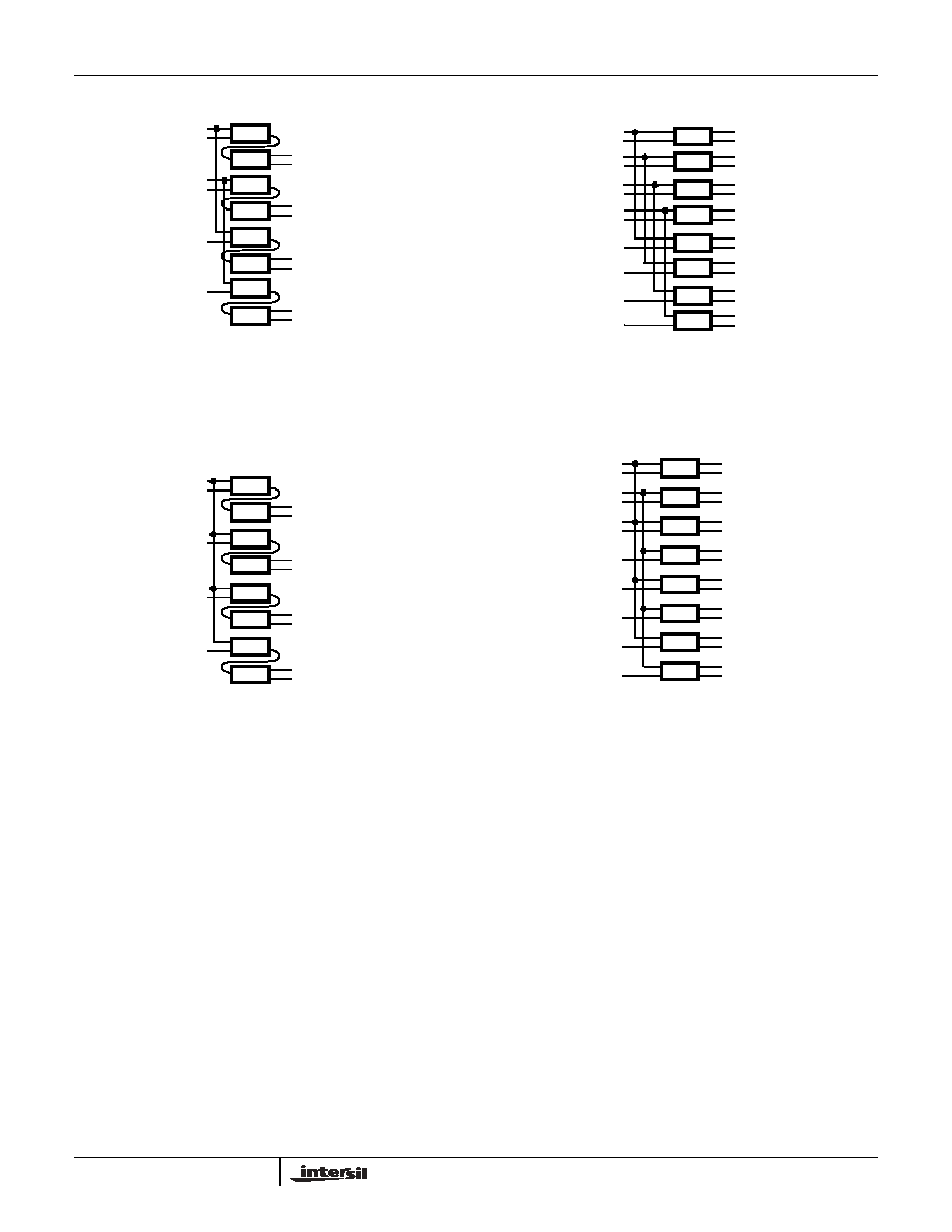
8-Bit Configurations
8-Bit Data, Single Row, 32 Sample Configurations
An 8 x 32 correlation also requires only 1 HSP45256. To
initialize the correlator, all the reference bits, control bits, the
value of the programmable delay, and the window configuration
must be specified. Table 12 details these settings.
Again, the loading of the reference and mask registers can
be done simultaneously. Due to the programming
initialization, DREF0-7 are used to load the reference data 8-
bits at a time. It will take 32 load pulses each of RLOAD and
CLOAD to load both arrays. Upon completion of the mask
and register loading, TXFR is pulsed low, which transfers the
reference and control data from the preload registers to the
registers that store the active data.
This configuration performs correlation of an 8-bit number
with a 1-bit reference. Each byte out of the correlation array
gives an 8-bit level of confidence that the data corresponds
to the reference. The correlation score is the sum of these
confidence levels.
TABLE 12. REGISTER LOADING FOR 8 X 32 CORRELATOR
WITH BINARY WEIGHTING
A0-2
DCONT0-7
NOTES
001
00001111
1 256-tap correlator; 8 x 32 window configu-
ration, 8-bit data stream; reference register is
loaded from DREF7 for all stages. Correlator
score = (128 x CO7) + (64 x CO3) + (32 x
CO5) + (16 x CO1) + (8 x CO6) + (4 x CO4)
+ (2 x CO2) + CO0.
010
00000000
Offset Register A = 0000000010000.
011
00010000
100
00000000
Programmable Delay = 0.
101
00000000
Offset Register B = 0 (Loading optional in
this mode).
110
00000000
7
6
5
4
3
2
1
0
REF <7>
DATA <7>
REFOUT <0>
DATAOUT <0>
CS = 128CO7+64CO6+32CO5+16CO4+8CO3+4CO2+2CO1+CO0
REFOUT <4>
DATAOUT <4>
DATA <3>
REFOUT <6>
DATAOUT <6>
REFOUT <2>
DATAOUT <2>
DATA <1>
DATA <5>
DATA <6>
DATA <4>
DATA <2>
DATA <0>
REFOUT <7>
DATAOUT <7>
REFOUT <5>
DATAOUT <5>
REFOUT <3>
DATAOUT <3>
REFOUT <1>
DATAOUT <1>
FIGURE 14. 8 BITS, 1 ROW OF 32 TAPS
HSP45256
17
Dual Correlator Configurations
1-Bit, Single Row, 128 Sample Configuration
FIGURE 15. DUAL 1-BIT, 1 ROW OF 128 TAPS
1-Bit, Dual Row, 64 Sample Configuration
FIGURE 16. 1-BIT, 2 ROWS OF 64 TAPS
1-Bit, Quad Row, 32 Sample Configuration
FIGURE 17. 1-BIT, 4 ROWS OF 32 TAPS
7
6
5
4
REF <7>
DATA <7>
DATAOUT <7>
CSA = (CO7+CO6+CO5+CO4); (CASOUT)
3
2
1
0
REF <3>
DATA <3>
DATAOUT <3>
CSB = (CO3+CO2+CO1+CO0); (AUXOUT)
7
6
5
4
REF <7>
DATA <7>
DATAOUT <5>
CSA = (CO7+CO6+CO5+CO4); (CASOUT)
DATAOUT <7>
REF <5>
DATA <5>
3
2
1
0
REF <3>
DATA <3>
DATAOUT <1>
CSB = (CO3+CO2+CO1+CO0); (AUXOUT)
DATAOUT <3>
REF <1>
DATA <1>
7
6
5
4
REF <7>
DATA <7>
DATAOUT <4>
CSA = (CO7+CO6+CO5+CO4); (CASOUT)
DATAOUT <6>
REF <5>
DATA <5>
DATAOUT <7>
REF <6>
DATA <6>
DATAOUT <5>
REF <4>
DATA <4>
3
2
1
0
REF <3>
DATA <3>
DATAOUT <0>
CSB = (CO3+CO2+CO1+CO0); (AUXOUT)
DATAOUT <2>
REF <1>
DATA <1>
DATAOUT <3>
REF <2>
DATA <2>
DATAOUT <1>
REF <0>
DATA <0>
HSP45256
18
2-Bit, Dual Row, 64 Sample Configuration
Dual 2 x 64 correlators require only one HSP45256. To
initialize the correlator, all the reference bits, control bits,
the delay value of the variable delay, and the window
configuration must be specified. Table 13 details the
settings for the 2-bit Dual Row, 64 Sample Configuration.
In this example, each of the dual correlators compares 2-bit
data to a 1-bit reference. It will take 64 load pulses
(RLOAD/CLOAD) to completely load the reference and
mask registers in the array. The programmable delay must
be set to 0 for the output of the two correlators to be aligned.
7
6
5
4
3
2
1
0
REF <7>
DATA <7>
CSA = 2(CO7+CO6)+CO5+CO4); (CASOUT)
REF <3>
DATA <3>
DATA <5>
DATA <1>
DATAOUT <7>
DATAOUT <5>
DATAOUT <3>
DATAOUT <1>
CSB = 2(CO3+CO2)+CO1+CO0); (AUXOUT)
FIGURE 18. 2-BITS, 1 ROW OF 64 TAPS
TABLE 13. REGISTER LOADING FOR DUAL 2 X 64 CORRELATORS WITH EQUAL WEIGHTING
AO-2
DCONT0-7
NOTES
001
00010110
Dual correlators: Each 2 bit data, 64 taps; reference register for correlation A is loaded from DREF7 and DREF5, the
reference register for correlator B is loaded from DREF3 and DREF1. Correlator #1 = 2x C07 + 2 x CO6 + CO5 + CO4,
correlator #2 = 2 x CO3 + 2x CO2 + CO1 + CO0.
010
00000000
Offset Register A = 0000000010000.
011
00010000
100
00000000
Programmable Delay = 0.
101
00000000
Offset Register B = 0.
110
00000000
2-Bit, Dual Row, 32 Sample Configuration
FIGURE 19. 2-BITS, 2 ROWS OF 32 TAPS
4-Bit, Single Row, 32 Sample Configuration
FIGURE 20. 4-BITS, 1 ROW OF 32 TAPS
7
6
5
4
3
2
1
0
REF <7>
DATA <7>
DATAOUT <0>
REF <3>
DATA <3>
REF <6>
DATA <6>
DATAOUT <2>
DATA <1>
DATAOUT <7>
DATAOUT <5>
DATAOUT <3>
DATAOUT <1>
REF <2>
DATA <2>
DATA <0>
CSA = 2(CO7+CO6)+CO5+CO4); (CASOUT)
CSB = 2(CO3+CO2)+CO1+CO0); (AUXOUT)
DATAOUT <6>
DATAOUT <4>
DATA <5>
DATA <4>
7
6
5
4
REF <7>
DATA <7>
DATAOUT <4>
CSA = 8(CO7)+4(CO6)+2(CO5)+(CO4); (CASOUT)
DATAOUT <5>
DATA <5>
DATAOUT <7>
DATAOUT <5>
DATA <4>
DATA <6>
3
2
1
0
REF <3>
DATA <3>
DATAOUT <0>
CSB = 8(CO3)+4(CO2)+2(CO1)+(CO0); (AUXOUT)
DATAOUT <2>
DATA <1>
DATAOUT <3>
DATAOUT <1>
DATA <0>
DATA <2>
HSP45256
19
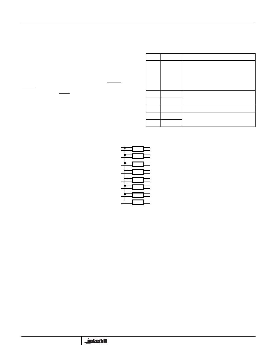
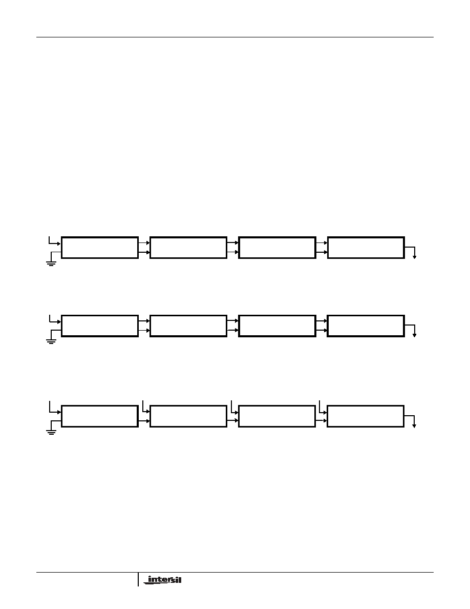
Cascading Multiple Correlator Devices
Correlators can be cascaded in either a serial or parallel
fashion. Longer correlations can be achieved by connecting
several correlators together as shown in Figures 21- 23. In
Figure 21, each correlator is in a one data bit, one row, 256
tap configuration. The number of bits of significance at the
CASOUT output of each correlator builds up from one
correlation to the next, that is, the maximum score out of the
first correlator is 256, the maximum output of the second
correlator is 512, etc. In this configuration, the maximum
length of the correlation is 4096. This would be implemented
with 16 HSP45256's. The Programmable Delay Register in
the first correlator would be set for one delay, the second
would be set for two, and so on, with the final HSP45256
being set for a delay of 16.
Correlations of more bits can be calculated by connecting
CASOUT of each chip to the CASIN of the following chip
(Figure 21). The data on the CASOUT lines accumulates in
a similar manner as in the 1 x 256 mode, except that the
maximum output of the first correlator is decimal 960,
(hexadecimal 3C0); in the general case, the maximum
number of correlators that can be cascaded in this manner is
eight, since the maximum output of the last one would be
1E00, which nearly uses up the 13-bit range of the cascade
summer. More parts could be cascaded together if some bits
are to be masked out or if the user has a prior knowledge of
the maximum value of the correlation score. As before, the
delay in the first correlator would be set to one, the second
correlator would be set for a delay of two, and so on.
Multiple HSP45256's can be cascaded for two dimensional
one bit data (Figure 22). The maximum output for each chip
is the same as in the 1 x 256 case; the only difference is in
the manner in which the correlators are connected. The
programmable delay registers would be set as before.
FIGURE 21. 1-BIT, 1024 SAMPLE CONFIGURATION
FIGURE 22. 4-BIT, 256 SAMPLE CONFIGURATION
FIGURE 23. 1-BIT, 32 x 32 WINDOW CONFIGURATION
CORRELATOR
SCORE
OUTPUT
DIN7
CASIN0-12
CASOUT0-12
DOUT7
DATA INPUT
DIN7
CASIN0-12
CASOUT0-12
DOUT7
DIN7
CASIN0-12
CASOUT0-12
DOUT7
DIN7
CASIN0-12
CASOUT0-12
DOUT7
CORRELATOR
SCORE
OUTPUT
DIN7, 5, 3, 1
CASIN0-12
CASOUT0-12
DOUT7, 5, 3, 1
DATA INPUT
DIN7, 5, 3, 1
CASIN0-12
CASOUT0-12
DOUT7, 5, 3, 1
DIN7, 5, 3, 1
CASIN0-12
CASOUT0-12
DOUT7, 5, 3, 1
DIN7, 5, 3, 1
CASIN0-12
CASOUT0-12
DOUT7, 5, 3, 1
CORRELATOR
SCORE
OUTPUT
DIN0-7
CASIN0-12
CASOUT0-12
DATA INPUT
DIN0-7
CASIN0-12
CASOUT0-12
DIN0-7
CASIN0-12
CASOUT0-12
DIN0-7
CASIN0-12
CASOUT0-12
ROWS 0 - 7
DATA INPUT
ROWS 8 - 15
DATA INPUT
ROWS 16 - 23
DATA INPUT
ROWS 24 - 31
HSP45256
20
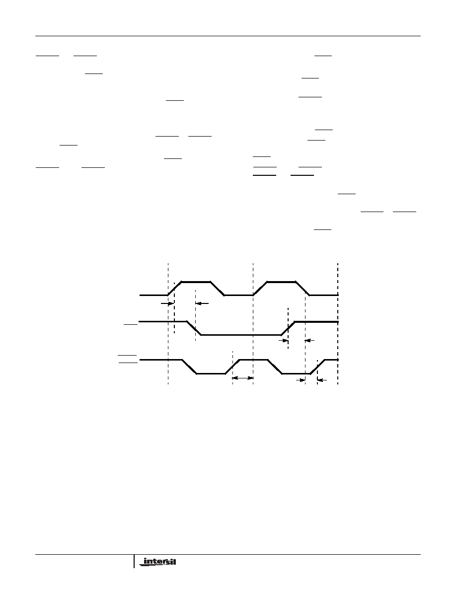
Reloading Data During Operation
RLOAD and CLOAD are asynchronous signals that are
designed to be driven by the memory interface signals of a
microprocessor. TXFR is synchronized to CLK so that the
mask or reference data is updated on a specific clock cycle.
In the normal mode of operation, the user loads the
reference and mask memories, then pulses TXFR to use
that data. The correlator uses the new mask or reference
information immediately. Loading of the reference and mask
data remains asynchronous as long as there is at least one
cycle of CLK between the rising edge of RLOAD or CLOAD
and the TXFR pulse.
If the system timing makes it necessary for TXFR and
RLOAD and/or CLOAD to be active during the same clock
cycle, then they must be treated as synchronous signals; the
timing for this case is shown in Figure 24 and given in the
AC Timing Specifications (t
THCL
and t
CLLH
). In this
example, data is loaded during clock cycle 1 and transferred
on the rising edge of CLK that occurs in clock cycle two.
Another set of data is loaded during clock cycle 2, which will
be transferred by a later TXFR pulse. The sequence of
events is as follows:
1. In clock cycle 1, TXFR becomes active at least t
TH
nano-
seconds after the rising edge of CLK.
2. RLOAD and/or CLOAD pulses low; the timing is not
critical as long as its rising edge occurs before the end of
clock cycle 1. If this condition is not met, it is undeter-
mined whether the data loaded by this pulse will be trans-
ferred by the current TXFR pulse.
3. The rising edge of TXFR occurs while CLK is high during
clock cycle 2. The margin between the rising edge of
TXFR and the falling edge of CLK is defined by t
THCL
.
4. RLOAD and/or CLOAD pulses low. The rising edge of
RLOAD and CLOAD must occur after the falling edge of
CLK. The margin between the two is defined by t
CLLH
.
The time from the rising edge of TXFR to the falling edge of
CLK must be greater than t
THCL
, and the time from the
falling edge of CLK to the rising edge of RLOAD or CLOAD
must be greater than t
s
. If this timing is violated, the data
being transferred by the TXFR pulse shown may or may not
include the data loaded in clock cycle 2.
CLK
TXFR
RLOAD,
CLOAD
CLOCK CYCLE 1
CLOCK CYCLE 2
FIGURE 24. LOADING AND TRANSFERRING DATA DURING THE SAME CLOCK CYCLE
t
TH
1.
2.
t
THCL
3.
t
CLLH
4.
HSP45256
21
Absolute Maximum Ratings
Thermal Information
Supply Voltage. . . . . . . . . . . . . . . . . . . . . . . . . . . . . . . . . . . . . +8.0V
Input, Output or I/O Voltage. . . . . . . . . . . . GND -0.5V to V
CC
+0.5V
ESD Classification . . . . . . . . . . . . . . . . . . . . . . . . . . . . . . . . . Class 1
Operating Conditions
Voltage Range . . . . . . . . . . . . . . . . . . . . . . . . . . . . +4.75V to +5.25V
Temperature Range
Commercial . . . . . . . . . . . . . . . . . . . . . . . . . . . . . . . . 0
o
C to 70
o
C
Industrial. . . . . . . . . . . . . . . . . . . . . . . . . . . . . . . . . -40
o
C to 85
o
C
Thermal Resistance (Typical, Note 1)
JA
(
o
C/W)
JC
(
o
C/W)
PLCC Package. . . . . . . . . . . . . . . . . . .
34
-
PGA Package. . . . . . . . . . . . . . . . . . . .
36
10
Maximum Package Power Dissipation
Commercial PGA . . . . . . . . . . . . . . . . . . . . . . . . . . . . . . . . . .2.9W
Commercial PLCC . . . . . . . . . . . . . . . . . . . . . . . . . . . . . . . . .2.3W
Industrial PLCC . . . . . . . . . . . . . . . . . . . . . . . . . . . . . . . . . . .1.9W
Maximum Storage Temperature Range . . . . . . . . . -65
o
C to 150
o
C
Maximum Junction Temperature
PLCC . . . . . . . . . . . . . . . . . . . . . . . . . . . . . . . . . . . . . . . . . .150
o
C
PGA . . . . . . . . . . . . . . . . . . . . . . . . . . . . . . . . . . . . . . . . . . . 175
o
C
Maximum Lead Temperature (Soldering 10s) . . . . . . . . . . . . . 300
o
C
Gate Count . . . . . . . . . . . . . . . . . . . . . . . . . . . . . . . . . 13,000 Gates
CAUTION: Stresses above those listed in "Absolute Maximum Ratings" may cause permanent damage to the device. This is a stress only rating and operation of the
device at these or any other conditions above those indicated in the operational sections of this specification is not implied.
NOTE:
1.
JA
is measured with the component mounted on an evaluation PC board in free air.
DC Electrical Specifications
PARAMETER
SYMBOL
TEST CONDITIONS
MIN
MAX
UNITS
Logical One Input Voltage
V
IH
V
CC
= 5.25V
2.0
-
V
Logical Zero Input Voltage
V
IL
V
CC
= 4.75V
-
0.8
V
High Level Clock Input
V
IHC
V
CC
= 5.25V
3.0
-
V
Low Level Clock Input
V
ILC
V
CC
= 4.75V
-
0.8
V
Output High Voltage
V
OH
I
OH
= 400
µ
A, V
CC
= 4.75V
2.6
-
V
Output Low Voltage
V
OL
I
OL
= +2.0mA, V
CC
= 4.75V
-
0.4
V
Input Leakage Current
I
I
V
IN
= V
CC
or GND, V
CC
= 5.25V
-10
10
µ
A
Output Leakage Current
I
O
V
OUT
= V
CC
or GND, V
CC
= 5.25V
-10
10
µ
A
Standby Power Supply Current
I
CCSB
V
IN
= V
CC
or GND, V
CC
= 5.25V
-
500
µ
A
Operating Power Supply Current
I
CCOP
f = 25.6MHz, V
IN
= V
CC
or GND, V
CC
= 5.25V,
Note 2, 4
-
179
mA
Capacitance
T
A
= 25
o
C, Note 3
PARAMETER
SYMBOL
MIN
MAX
UNITS
TEST CONDITIONS
Input Capacitance
C
IN
-
10
pF
Frequency = 1MHz, V
CC
= Open
All measurements are referenced to device ground.
Output Capacitance
C
O
-
10
pF
NOTES:
2. Power supply current is proportional to operating frequency. Typical rating for I
CCOP
is 7mA/MHz.
3. Not tested, but characterized at initial design and at major process/design changes.
4. Output load per test load circuit and C
L
= 40pF.
AC Electrical Specifications
V
CC
= 5.0V
±
5%, T
A
= 0
o
C to 70
o
C, T
A
= -40
o
C to 85
o
C, Note 5
PARAMETER
SYMBOL
NOTES
33MHz
25.6MHz
UNITS
MIN
MAX
MIN
MAX
CLK Period
t
CP
30
-
39
-
ns
CLK High
t
CH
12
-
15
-
ns
CLK Low
t
CL
12
-
15
-
ns
HSP45256
22
Test Load Circuit
Set-Up Time DIN to CLK High
t
DS
12
-
13
-
ns
Hold Time CLK High to DIN
t
DH
0
-
0
-
ns
TXFR Set-Up Time
t
TS
12
-
13
-
ns
TXFR Hold Time
t
TH
0
-
0
-
ns
Output Delay DOUT, AUXOUT, CASOUT
t
DO
-
15
-
20
ns
CLOAD Cycle Time
t
CLC
30
-
39
-
ns
CLOAD High
t
CLH
12
-
15
-
ns
CLOAD Low
t
CLL
12
-
15
-
ns
Set-Up Time, A to RLOAD, CLOAD
t
AS
12
-
13
-
ns
Hold Time, RLOAD, CLOAD to A
t
AH
0
-
0
-
ns
RLOAD Cycle Time
t
RLC
30
-
39
-
ns
RLOAD High
t
RLH
12
-
15
-
ns
RLOAD Low
t
RLL
12
-
15
-
ns
Set-Up Time, DCONT to CLOAD
t
DCS
12
-
13
-
ns
Hold Time, CLOAD to DCONT
t
DCH
0
-
0
-
ns
Set-Up Time, DREF to RLOAD
t
RS
12
-
13
-
ns
Hold Time, RLOAD to DREF
t
RH
0
-
0
-
ns
Output Enable Time
t
OE
-
15
-
15
ns
Output Disable Time
t
OD
Note 6
-
15
-
15
ns
Output Rise, Fall Time
t
RF
Note 6
-
6
6
ns
TXFR High to CLK Low
t
THCL
Note 6
3
-
3
-
ns
CLK Low to RLOAD, CLOAD High
t
CLLH
Note 6
1
-
1
-
ns
NOTES:
5. AC testing is performed as follows: Input levels (CLK Input) 4.0V and 0V; Input levels (all other inputs) 0V and 3.0V; Timing reference levels
(CLK) 2.0V; All others 1.5V. Output load per test load circuit with C
L
= 40pF. Output transition is measured at V
OH
> 1.5V and
V
OL
< 1.5V.
6. Controlled via design or process parameters and not directly tested. Characterized upon initial design and after major process and/or design
changes.
AC Electrical Specifications
V
CC
= 5.0V
±
5%, T
A
= 0
o
C to 70
o
C, T
A
= -40
o
C to 85
o
C, Note 5 (Continued)
PARAMETER
SYMBOL
NOTES
33MHz
25.6MHz
UNITS
MIN
MAX
MIN
MAX
DUT
EQUIVALENT CIRCUIT
1.5V
I
OL
I
OH
C
L
INCLUDES STRAY
AND JIG
±
S
1
CAPACITANCE
SWITCH S
1
OPEN FOR I
CCSB
AND I
CCOP
TEST
HSP45256
23
All Intersil U.S. products are manufactured, assembled and tested utilizing ISO9000 quality systems.
Intersil Corporation's quality certifications can be viewed at www.intersil.com/design/quality
Intersil products are sold by description only. Intersil Corporation reserves the right to make changes in circuit design, software and/or specifications at any time without
notice. Accordingly, the reader is cautioned to verify that data sheets are current before placing orders. Information furnished by Intersil is believed to be accurate and
reliable. However, no responsibility is assumed by Intersil or its subsidiaries for its use; nor for any infringements of patents or other rights of third parties which may result
from its use. No license is granted by implication or otherwise under any patent or patent rights of Intersil or its subsidiaries.
For information regarding Intersil Corporation and its products, see www.intersil.com
Timing Waveforms
FIGURE 25. INPUT, OUTPUT TIMING
FIGURE 26. CONTROL INPUT TIMING
FIGURE 27. REFERENCE INPUT TIMING
FIGURE 28. OUTPUT TIMING
FIGURE 29. TRANSFER, LOAD TIMING WHEN BOTH OCCUR ON A SINGLE CYCLE
CLK
DIN0-7
TXFR
DOUT0-7
CASOUT0-12,
AUXOUT0-8
t
CP
t
CL
t
CH
t
DH
t
DS
t
TS
t
TH
t
TS
t
DO
CLOAD
A0-2
t
CLC
t
CLL
t
CLH
t
AH
t
AS
DCONT0-7
t
CH
t
CS
DLOAD
A0-2
t
RLC
t
RLH
t
RLL
t
AH
t
AS
DREF0-7
t
RH
t
RS
t
r
, t
f
2.0V
0.8V
t
OE
1.7V
1.3V
OEA, OEC
t
OD
AUXOUT0-8
CASOUT0-12
DOUT0-7,
CASOUT0-12,
AUXOUT0-8
t
THCL
t
CLLH
CLK
TXFR
RLOAD,
CLOAD
HSP45256