
1
Æ
FN3093.3
ICL7135
4
1
/
2
Digit, BCD Output, A/D Converter
The Intersil ICL7135 precision A/D converter, with its
multiplexed BCD output and digit drivers, combines dual-
slope conversion reliability with
±
1 in 20,000 count accuracy
and is ideally suited for the visual display DVM/DPM market.
The 2.0000V full scale capability, auto-zero, and auto-
polarity are combined with true ratiometric operation, almost
ideal differential linearity and true differential input. All
necessary active devices are contained on a single CMOS
lC, with the exception of display drivers, reference, and a
clock.
The ICL7135 brings together an unprecedented combination
of high accuracy, versatility, and true economy. It features
auto-zero to less than 10
µ
V, zero drift of less than 1
µ
V/
o
C,
input bias current of 10pA (Max), and rollover error of less
than one count. The versatility of multiplexed BCD outputs is
increased by the addition of several pins which allow it to
operate in more sophisticated systems. These include
STROBE, OVERRANGE, UNDERRANGE, RUN/HOLD and
BUSY lines, making it possible to interface the circuit to a
microprocessor or UART.
Features
∑ Accuracy Guaranteed to
±
1 Count Over Entire
±
20000
Counts (2.0000V Full Scale)
∑ Guaranteed Zero Reading for 0V Input
∑ 1pA Typical Input Leakage Current
∑ True Differential Input
∑ True Polarity at Zero Count for Precise Null Detection
∑ Single Reference Voltage Required
∑ Overrange and Underrange Signals Available for Auto-
Range Capability
∑ All Outputs TTL Compatible
∑ Blinking Outputs Gives Visual Indication of Overrange
∑ Six Auxiliary Inputs/Outputs are Available for Interfacing to
UARTs, Microprocessors, or Other Circuitry
∑ Multiplexed BCD Outputs
∑
Pb-Free Available (RoHS Compliant)
Pinout
ICL7135
(PDIP)
TOP VIEW
Ordering Information
PART NUMBER
TEMP.
RANGE (∞C)
PACKAGE
PKG.
DWG. #
ICL7135CPI
0 to 70
28 Ld PDIP
E28.6
ICL7135CPIZ
(Note 1)
0 to 70
28 Ld PDIP
(Pb-free) (Note 2)
E28.6
NOTES:
1. Intersil Pb-free products employ special Pb-free material sets;
molding compounds/die attach materials and 100% matte tin
plate termination finish, which are RoHS compliant and
compatible with both SnPb and Pb-free soldering operations.
Intersil Pb-free products are MSL classified at Pb-free peak
reflow temperatures that meet or exceed the Pb-free
requirements of IPC/JEDEC J STD-020C.
2. Pb-free PDIPs can be used for through hole wave solder
processing only. They are not intended for use in Reflow solder
processing applications.
V-
REFERENCE
NALOG COMMON
INT OUT
AZ IN
BUFF OUT
REF CAP -
REF CAP +
IN LO
IN HI
V+
(MSD) D5
(LSB) B1
B2
UNDERRANGE
STROBE
R/H
DIGITAL GND
POL
BUSY
D2
D3
D4
(MSB) B8
B4
OVERRANGE
CLOCK IN
(LSD) D1
28
27
26
25
24
23
22
21
20
19
18
17
16
15
1
2
3
4
5
6
7
8
9
10
11
12
13
14
Data Sheet
October 25, 2004
CAUTION: These devices are sensitive to electrostatic discharge; follow proper IC Handling Procedures.
1-888-INTERSIL or 321-724-7143
|
Intersil (and design) is a registered trademark of Intersil Americas Inc.
Copyright Intersil Americas Inc. 2000, 2004. All Rights Reserved
All other trademarks mentioned are the property of their respective owners.

2
FN3093.3
Typical Application Schematic
28
27
26
25
23
22
21
20
19
18
17
16
15
1
2
3
4
5
6
7
8
9
10
11
12
13
14
24
SET V
REF
= 1.000V
V
REF
IN
SIGNAL
-5V
+5V
100k
27
100k
100K
ANALOG
GND
INPUT
1
µ
F
0.47
µ
F
1
µ
F
0.1
µ
F
100k
ICL7135
CLOCK IN
120kHz
0V
6
ANODE
DRIVER
TRANSISTORS
SEVEN
SEG.
DECODE
DISPLAY
ICL7135
3
FN3093.3
Absolute Maximum Ratings
Thermal Information
Supply Voltage V+ . . . . . . . . . . . . . . . . . . . . . . . . . . . . . . . . . . . .+6V
V- . . . . . . . . . . . . . . . . . . . . . . . . . . . . . . . . . . . -9V
Analog Input Voltage (Either Input) (Note 1) . . . . . . . . . . . . V+ to V-
Reference Input Voltage (Either Input). . . . . . . . . . . . . . . . . V+ to V-
Clock Input Voltage . . . . . . . . . . . . . . . . . . . . . . . . . . . . . GND to V+
Operating Conditions
Temperature Range . . . . . . . . . . . . . . . . . . . . . . . . . . . . 0
o
C to 70
o
C
Thermal Resistance (Typical, Note 2) . . . . . . . . . . . . .
JA
(
o
C/W)
PDIP Package . . . . . . . . . . . . . . . . . . . . . . . . . . . . .
55
Maximum Junction Temperature . . . . . . . . . . . . . . . . . . . . . . . 150
o
C
Maximum Storage Temperature Range . . . . . . . . . . -65
o
C to 150
o
C
Maximum Lead Temperature (Soldering 10s) . . . . . . . . . . . . . 300
o
C
NOTE: Pb-free PDIPs can be used for through hole wave solder
processing only. They are not intended for use in Reflow solder
processing applications.
CAUTION: Stresses above those listed in "Absolute Maximum Ratings" may cause permanent damage to the device. This is a stress only rating and operation of the
device at these or any other conditions above those indicated in the operational sections of this specification is not implied.
NOTES:
1. Input voltages may exceed the supply voltages provided the input current is limited to +100
µ
A.
2.
JA
is measured with the component mounted on a low effective thermal conductivity test board in free air. See Tech Brief TB379 for details.
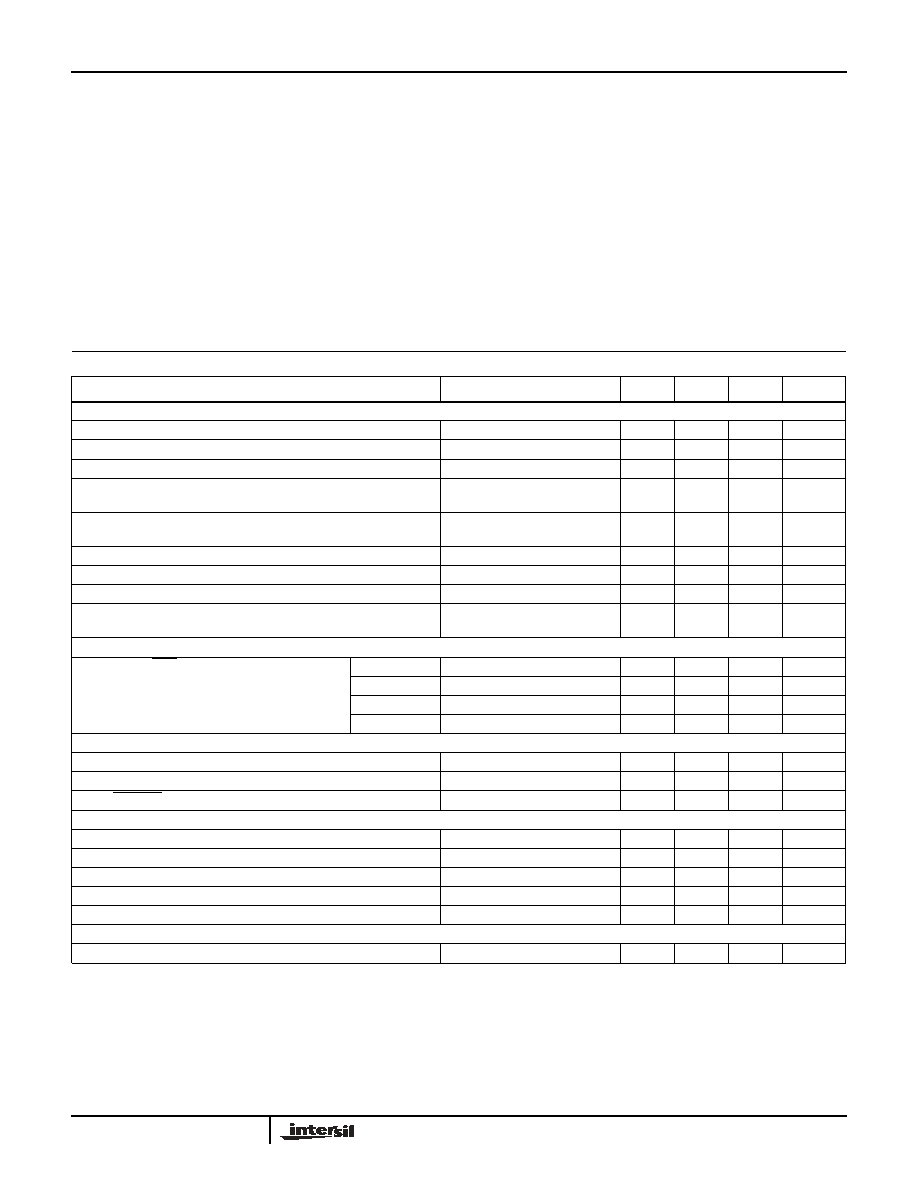
Electrical Specifications
V+ = +5V, V- = -5V, T
A
= 25
o
C, f
CLK
Set for 3 Readings/s, Unless Otherwise Specified
PARAMETER
TEST CONDITIONS
MIN
TYP
MAX
UNITS
ANALOG (Notes 3, 4)
Zero Input Reading
V
lN
= 0V, V
REF
= 1.000V
-00000
+00000
+00000
Counts
Ratiometric Error (Note 4)
V
lN
= V
REF
= 1.000V
-3
0
+3
Counts
Linearity Over
±
Full Scale (Error of Reading from Best Straight Line)
-2V
V
IN
+2V
-
0.5
1
LSB
Differential Linearity (Difference Between Worse Case Step of
Adjacent Counts and Ideal Step)
-2V
V
IN
+2V
-
0.01
-
LSB
Rollover Error (Difference in Reading for Equal Positive and
Negative Voltage Near Full Scale)
-V
lN
+V
lN
2V
-
0.5
1
LSB
Noise (Peak-to-Peak Value Not Exceeded 95% of Time), e
N
V
lN
= 0V, Full scale = 2.000V
-
15
-
µ
V
Input Leakage Current, I
ILK
V
lN
= 0V
-
1
10
pA
Zero Reading Drift (Note 7)
V
lN
= 0V, 0
o
C to 70
o
C
-
0.5
2
µ
V/
o
C
Scale Factor Temperature Coefficient, T
C
(Notes 5 and 7)
V
lN
= +2V, 0
o
C to 70
o
C
Ext. Ref. 0ppm/
o
C
-
2
5
ppm/◊
o
C
DIGITAL INPUTS
Clock In, Run/Hold (See Figure 2)
V
INH
2.8
2.2
-
V
V
INL
-
1.6
0.8
V
I
INL
V
IN
= 0V
-
0.02
0.1
mA
I
INH
V
IN
= +5V
-
0.1
10
µ
A
DIGITAL OUTPUTS
All Outputs, V
OL
I
OL
= 1.6mA
-
0.25
0.40
V
B1 , B2 , B4 , B8 , D1 , D2 , D3 , D4 , D5 , V
OH
I
OH
= -1mA
2.4
4.2
-
V
BUSY, STROBE, OVERRANGE, UNDERRANGE, POLARITY, V
OH
I
OH
= -10
µ
A
4.9
4.99
-
V
SUPPLY
+5V Supply Range, V+
+4
+5
+6
V
-5V Supply Range, V-
-3
-5
-8
V
+5V Supply Current, I+
f
C
= 0
-
1.1
3.0
mA
-5V Supply Current, I-
f
C
= 0
-
0.8
3.0
mA
Power Dissipation Capacitance, C
PD
vs Clock Frequency
-
40
-
pF
CLOCK
Clock Frequency (Note 6)
DC
2000
1200
kHz
NOTES:
3. Tested in 4
1
/
2
digit (20.000 count) circuit shown in Figure 3. (Clock frequency 120kHz.)
4. Tested with a low dielectric absorption integrating capacitor, the 27
INT OUT resistor shorted, and R
lNT
= 0. See Component Value Selection Discussion.
5. The temperature range can be extended to 70
o
C and beyond as long as the auto-zero and reference capacitors are increased to absorb the higher leakage
of the ICL7135.
6. This specification relates to the clock frequency range over which the lCL7135 will correctly perform its various functions See "Max Clock Frequency"
section for limitations on the clock frequency range in a system.
7. Parameter guaranteed by design or characterization. Not production tested.
ICL7135

4
FN3093.3
FIGURE 1. ICL7135 TEST CIRCUIT
FIGURE 2. ICL7135 DIGITAL LOGIC INPUT
FIGURE 3. ANALOG SECTION OF ICL7135
28
27
26
25
23
22
21
20
19
18
17
16
15
1
2
3
4
5
6
7
8
9
10
11
12
13
14
24
SET V
REF
= 1.000V
V
REF
IN
SIGNAL
-5V
+5V
100k
27
100k
100K
ANALOG
GND
INPUT
1
µ
F
0.47
µ
F
1
µ
F
0.1
µ
F
100k
ICL7135
0V
CLOCK
IN
120kHz
UNDERRANGE
OVERRANGE
STROBE
RUN/HOLD
DIGITAL GND
POLARITY
CLOCK IN
BUSY
LSD DI
D2
D3
D4
MSB B8
B4
V-
REF
ANALOG GND
INT OUT
A-Z IN
BUF OUT
REF CAP 1
REF CAP 2
IN LO-
IN HI+
V+
MSD D5
LSB B1
B2
V
+
PAD
DIG GND
C
REF+
REF HI
IN HI
INT
A/Z
ANALOG
AZ
IN LO
ZI
C
REF
BUFFER
COMMON
INPUT
COMPARATOR
C
AZ
C
INT
R
INT
INTEGRATOR
INPUT
V
+
V
-
POLARITY
ZERO-
LOW
HIGH
CROSSING
DETECTOR
F/F
DE(+)
DE(-)
DE(-)
DE(+)
AZ
AZ
AUTO
ZERO
INT
1
2
3
4
5
6
11
10
9
8
7
-
+
-
+
+
C
REF
A/Z, DE(
±
), ZI
INT
ICL7135

5
FN3093.3
Detailed Description
Analog Section
Figure 3 shows the Block Diagram of the Analog Section for
the ICL7135. Each measurement cycle is divided into four
phases. They are (1) auto-zero (AZ), (2) signal-integrate
(INT), (3) de-integrate (DE) and (4) zero-integrator (Zl).
Auto-Zero Phase
During auto-zero, three things happen. First, input high and low
are disconnected from the pins and internally shorted to analog
COMMON. Second, the reference capacitor is charged to the
reference voltage. Third, a feedback loop is closed around the
system to charge the auto-zero capacitor C
AZ
to compensate
for offset voltages in the buffer amplifier, integrator, and
comparator. Since the comparator is included in the loop, the
AZ accuracy is limited only by the noise of the system. In any
case, the offset referred to the input is less than 10
µ
V.
Signal Integrate Phase
During signal integrate, the auto-zero loop is opened, the
internal short is removed, and the internal input high and low
are connected to the external pins. The converter then
integrates the differential voltage between IN HI and IN LO for a
fixed time. This differential voltage can be within a wide
common mode range; within one volt of either supply. If, on the
other hand, the input signal has no return with respect to the
converter power supply, IN LO can be tied to analog COMMON
to establish the correct common-mode voltage. At the end of
this phase, the polarity of the integrated signal is latched into
the polarity F/F.
De-Integrate Phase
The third phase is de-integrate or reference integrate. Input
low is internally connected to analog COMMON and input
high is connected across the previously charged reference
capacitor. Circuitry within the chip ensures that the capacitor
will be connected with the correct polarity to cause the inte-
grator output to return to zero. The time required for the out-
put to return to zero is proportional to the input signal.
Specifically the digital reading displayed is:
.
Zero Integrator Phase
The final phase is zero integrator. First, input low is shorted
to analog COMMON. Second, a feedback loop is closed
around the system to input high to cause the integrator
output to return to zero. Under normal condition, this phase
lasts from 100 to 200 clock pulses, but after an overrange
conversion, it is extended to 6200 clock pulses.
Differential Input
The input can accept differential voltages anywhere within the
common mode range of the input amplifier; or specifically
from 0.5V below the positive supply to 1V above the negative
supply. In this range the system has a CMRR of 86dB typical.
However, since the integrator also swings with the common
mode voltage, care must be exercised to assure the integrator
output does not saturate. A worst case condition would be a
large positive common-mode voltage with a near full scale
negative differential input voltage. The negative input signal
drives the integrator positive when most of its swing has been
used up by the positive common mode voltage. For these
critical applications the integrator swing can be reduced to
less than the recommended 4V full scale swing with some
loss of accuracy. The integrator output can swing within 0.3V
of either supply without loss of linearity.
Analog COMMON
Analog COMMON is used as the input low return during auto-
zero and de-integrate. If IN LO is different from analog
COMMON, a common mode voltage exists in the system and
is taken care of by the excellent CMRR of the converter.
However, in most applications IN LO will be set at a fixed
known voltage (power supply common for instance). In this
application, analog COMMON should be tied to the same
point, thus removing the common mode voltage from the
converter. The reference voltage is referenced to analog
COMMON.
Reference
The reference input must be generated as a positive voltage
with respect to COMMON, as shown in Figure 4.
OUTPUT COUNT
10,000
V
IN
V
REF
---------------
=
FIGURE 4A.
FIGURE 4B.
FIGURE 4. USING AN EXTERNAL REFERENCE
I
Z
6.8V
V-
ZENER
REF HI
ICL7135
COMMON
V+
6.8k
ICL8069
REF HI
ICL7135
COMMON
V+
V+
20k
1.2V
REFERENCE
ICL7135