
3-26
File Number
3072.4
ICL7660, ICL7660A
CMOS Voltage Converters
The Intersil ICL7660 and ICL7660A are monolithic CMOS
power supply circuits which offer unique performance
advantages over previously available devices. The ICL7660
performs supply voltage conversions from positive to
negative for an input range of +1.5V to +10.0V resulting in
complementary output voltages of -1.5V to -10.0V and the
ICL7660A does the same conversions with an input range of
+1.5V to +12.0V resulting in complementary output voltages
of -1.5V to -12.0V. Only 2 noncritical external capacitors are
needed for the charge pump and charge reservoir functions.
The ICL7660 and ICL7660A can also be connected to
function as voltage doublers and will generate output
voltages up to +18.6V with a +10V input.
Contained on the chip are a series DC supply regulator, RC
oscillator, voltage level translator, and four output power
MOS switches. A unique logic element senses the most
negative voltage in the device and ensures that the output N-
Channel switch source-substrate junctions are not forward
biased. This assures latchup free operation.
The oscillator, when unloaded, oscillates at a nominal
frequency of 10kHz for an input supply voltage of 5.0V. This
frequency can be lowered by the addition of an external
capacitor to the "OSC" terminal, or the oscillator may be
overdriven by an external clock.
The "LV" terminal may be tied to GROUND to bypass the
internal series regulator and improve low voltage (LV)
operation. At medium to high voltages (+3.5V to +10.0V for
the ICL7660 and +3.5V to +12.0V for the ICL7660A), the LV
pin is left floating to prevent device latchup.
Features
∑ Simple Conversion of +5V Logic Supply to
±
5V Supplies
∑ Simple Voltage Multiplication (V
OUT
= (-) nV
IN
)
∑ Typical Open Circuit Voltage Conversion Efficiency 99.9%
∑ Typical Power Efficiency 98%
∑ Wide Operating Voltage Range
- ICL7660 . . . . . . . . . . . . . . . . . . . . . . . . . . 1.5V to 10.0V
- ICL7660A . . . . . . . . . . . . . . . . . . . . . . . . . 1.5V to 12.0V
∑ ICL7660A 100% Tested at 3V
∑ Easy to Use - Requires Only 2 External Non-Critical
Passive Components
∑ No External Diode Over Full Temp. and Voltage Range
Applications
∑ On Board Negative Supply for Dynamic RAMs
∑ Localized
µ
Processor (8080 Type) Negative Supplies
∑ Inexpensive Negative Supplies
∑ Data Acquisition Systems
Pinouts
ICL7660, ICL7660A (PDIP, SOIC)
TOP VIEW
ICL7660 (METAL CAN)
TOP VIEW
Ordering Information
PART NO.
TEMP.
RANGE (
o
C)
PACKAGE
PKG.
NO.
ICL7660CBA
0 to 70
8 Ld SOIC (N)
M8.15
ICL7660CBA-T
0 to 70
8 Ld SOIC (N)
Tape and Reel
M8.15
ICL7660CPA
0 to 70
8 Ld PDIP
E8.3
ICL7660MTV
0 to 70
8 Pin Metal Can
T8.C
ICL7660ACBA
0 to 70
8 Ld SOIC (N)
M8.15
ICL7660ACBA-T
0 to 70
8 Ld SOIC (N)
Tape and Reel
M8.15
ICL7660ACPA
0 to 70
8 Ld PDIP
E8.3
ICL7660AIBA
-40 to 85
8 Ld SOIC (N)
M8.15
ICL7660AIBA-T
-40 to 85
8 Ld SOIC (N)
Tape and Reel
M8.15
ICL7660AIPA
-40 to 85
8 Ld PDIP
E8.3
Add /883B to part number if 883B processing is required.
NC
CAP+
GND
CAP-
1
2
3
4
8
7
6
5
V+
OSC
LV
V
OUT
V+ (AND CASE)
LV
CAP+
NC
GND
OSC
V
OUT
2
4
6
1
3
7
5
8
CAP-
Data Sheet
April 1999
CAUTION: These devices are sensitive to electrostatic discharge; follow proper IC Handling Procedures.
http://www.intersil.com or 407-727-9207
|
Copyright
©
Intersil Corporation 1999

3-27
C
Absolute Maximum Ratings
Thermal Information
Supply Voltage
ICL7660 . . . . . . . . . . . . . . . . . . . . . . . . . . . . . . . . . . . . . . . +10.5V
ICL7660A . . . . . . . . . . . . . . . . . . . . . . . . . . . . . . . . . . . . . . +13.0V
LV and OSC Input Voltage . . . . . . -0.3V to (V+ +0.3V) for V+ < 5.5V
(Note 2) . . . . . . . . . . . . . . (V+ -5.5V) to (V+ +0.3V) for V+ > 5.5V
Current into LV (Note 2) . . . . . . . . . . . . . . . . . . . 20
µ
A for V+ > 3.5V
Output Short Duration (V
SUPPLY
5.5V) . . . . . . . . . . . . Continuous
Operating Conditions
Temperature Range
ICL7660M. . . . . . . . . . . . . . . . . . . . . . . . . . . . . . . -55
o
C to 125
o
C
ICL7660C, ICL7660AC. . . . . . . . . . . . . . . . . . . . . . . . 0
o
C to 70
o
C
ICL7660AI . . . . . . . . . . . . . . . . . . . . . . . . . . . . . . . -40
o
C to 85
o
C
Thermal Resistance (Typical, Note 1)
JA
(
o
C/W)
JC
(
o
C/W)
PDIP Package . . . . . . . . . . . . . . . . . . .
150
N/A
SOIC Package . . . . . . . . . . . . . . . . . . .
165
N/A
Metal Can Package (ICL7660 Only). . .
160
70
Maximum Storage Temperature Range . . . . . . . . . . -65
o
C to 150
o
C
Maximum Lead Temperature (Soldering, 10s). . . . . . . . . . . . .300
o
C
(SOIC - Lead Tips Only)
CAUTION: Stresses above those listed in "Absolute Maximum Ratings" may cause permanent damage to the device. This is a stress only rating and operation of the
device at these or any other conditions above those indicated in the operational sections of this specification is not implied.
NOTE:
1.
JA
is measured with the component mounted on an evaluation PC board in free air.
Electrical Specifications
ICL7660 and ICL7660A, V+ = 5V, T
A
= 25
o
C, C
OSC
= 0, Test Circuit Figure 11
Unless Otherwise Specified
PARAMETER
SYMBOL
TEST CONDITIONS
ICL7660
ICL7660A
UNITS
MIN
TYP
MAX
MIN
TYP
MAX
Supply Current
I+
R
L
=
-
170
500
-
80
165
µ
A
Supply Voltage Range - Lo
V
L
+
MIN
T
A
MAX, R
L
= 10k
, LV to GND
1.5
-
3.5
1.5
-
3.5
V
Supply Voltage Range - Hi
V
H
+
MIN
T
A
MAX, R
L
= 10k
, LV to Open
3.0
-
10.0
3
-
12
V
Output Source Resistance
R
OUT
I
OUT
= 20mA, T
A
= 25
o
C
-
55
100
-
60
100
I
OUT
= 20mA, 0
o
C
T
A
70
o
C
-
-
120
-
-
120
I
OUT
= 20mA, -55
o
C
T
A
125
o
C
-
-
150
-
-
-
I
OUT
= 20mA, -40
o
C
T
A
85
o
C
-
-
-
-
-
120
V
+
= 2V, I
OUT
= 3mA, LV to GND
0
o
C
T
A
70
o
C
-
-
300
-
-
300
V+ = 2V, I
OUT
= 3mA, LV to GND,
-55
o
C
T
A
125
o
C
-
-
400
-
-
-
Oscillator Frequency
f
OSC
-
10
-
-
10
-
kHz
Power Efficiency
P
EF
R
L
= 5k
95
98
-
96
98
-
%
Voltage Conversion Efficiency
V
OUT EF
R
L
=
97
99.9
-
99
99.9
-
%
Oscillator Impedance
Z
OSC
V+ = 2V
-
1.0
-
-
1
-
M
V = 5V
-
100
-
-
-
-
k
ICL7660A, V+ = 3V, T
A
= 25
o
C, OSC = Free running, Test Circuit Figure 11, Unless Otherwise Specified
Supply Current (Note 3)
I+
V+ = 3V, R
L
=
, 25
o
C
-
-
-
-
26
100
µ
A
0
o
C < T
A
< 70
o
C
-
-
-
-
-
125
µ
A
-40
o
C < T
A
< 85
o
C
-
-
-
-
-
125
µ
A
Output Source Resistance
R
OUT
V+ = 3V, I
OUT
= 10mA
-
-
-
-
97
150
0
o
C < T
A
< 70
o
C
-
-
-
-
-
200
-40
o
C < T
A
< 85
o
C
-
-
-
-
-
200
Oscillator Frequency (Note 3)
f
OSC
V+ = 3V (same as 5V conditions)
-
-
-
5.0
8
-
kHz
0
o
C < T
A
< 70
o
C
-
-
-
3.0
-
-
kHz
-40
o
C < T
A
< 85
o
C
-
-
-
3.0
-
-
kHz
ICL7660, ICL7660A
3-28
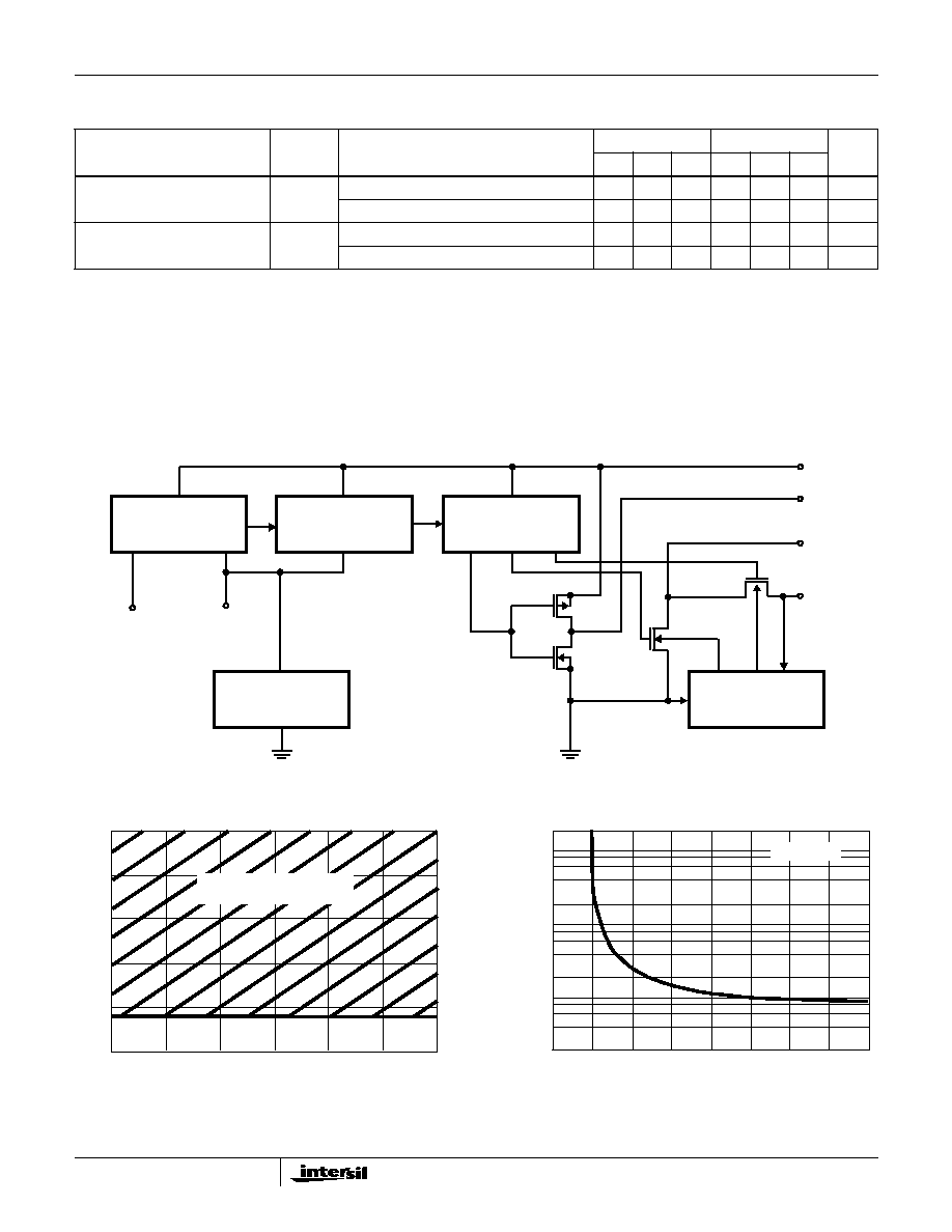
Functional Block Diagram
Voltage Conversion Efficiency
V
OUT
EFF V+ = 3V, R
L
=
-
-
-
99
-
-
%
T
MIN
< T
A
< T
MAX
-
-
-
99
-
-
%
Power Efficiency
P
EFF
V+ = 3V, R
L
= 5k
-
-
-
96
-
-
%
T
MIN
< T
A
< T
MAX
-
-
-
95
-
-
%
NOTES:
2. Connecting any input terminal to voltages greater than V+ or less than GND may cause destructive latchup. It is recommended that no inputs
from sources operating from external supplies be applied prior to "power up" of the ICL7660, ICL7660A.
3. Derate linearly above 50
o
C by 5.5mW/
o
C.
4. In the test circuit, there is no external capacitor applied to pin 7. However, when the device is plugged into a test socket, there is usually a very
small but finite stray capacitance present, of the order of 5pF.
5. The Intersil ICL7660A can operate without an external diode over the full temperature and voltage range. This device will function in existing
designs which incorporate an external diode with no degradation in overall circuit performance.
Electrical Specifications
ICL7660 and ICL7660A, V+ = 5V, T
A
= 25
o
C, C
OSC
= 0, Test Circuit Figure 11
Unless Otherwise Specified (Continued)
PARAMETER
SYMBOL
TEST CONDITIONS
ICL7660
ICL7660A
UNITS
MIN
TYP
MAX
MIN
TYP
MAX
RC
OSCILLATOR
˜
2
VOLTAGE
LEVEL
TRANSLATOR
VOLTAGE
REGULATOR
LOGIC
NETWORK
OSC
LV
V+
CAP+
CAP-
V
OUT
Typical Performance Curves
(Test Circuit of Figure 11)
FIGURE 1. OPERATING VOLTAGE AS A FUNCTION OF
TEMPERATURE
FIGURE 2. OUTPUT SOURCE RESISTANCE AS A FUNCTION
OF SUPPLY VOLTAGE
10
SUPPLY VOLTAGE RANGE
(NO DIODE REQUIRED)
8
6
4
2
0
-55
-25
0
25
50
100
125
TEMPERATURE (
o
C)
SUPPL
Y V
O
L
T
A
GE (V)
10K
T
A
= 25
o
C
1000
100
10
0
1
2
3
4
5
6
7
8
SUPPLY VOLTAGE (V+)
OUTPUT SOURCE RESIST
ANCE (
)
ICL7660, ICL7660A
3-29
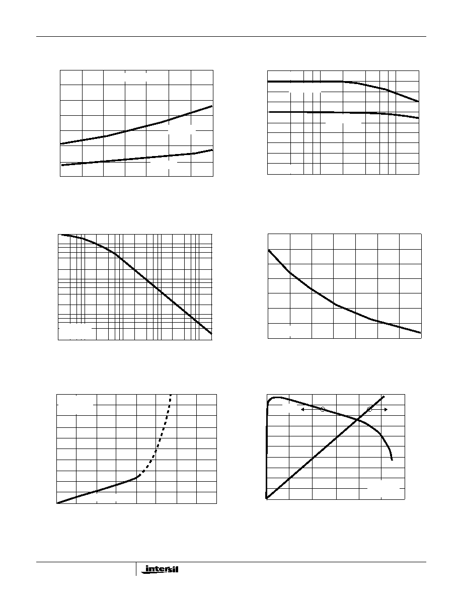
FIGURE 3. OUTPUT SOURCE RESISTANCE AS A FUNCTION
OF TEMPERATURE
FIGURE 4. POWER CONVERSION EFFICIENCY AS A
FUNCTION OF OSC. FREQUENCY
FIGURE 5. FREQUENCY OF OSCILLATION AS A FUNCTION
OF EXTERNAL OSC. CAPACITANCE
FIGURE 6. UNLOADED OSCILLATOR FREQUENCY AS A
FUNCTION OF TEMPERATURE
FIGURE 7. OUTPUT VOLTAGE AS A FUNCTION OF OUTPUT
CURRENT
FIGURE 8. SUPPLY CURRENT AND POWER CONVERSION
EFFICIENCY AS A FUNCTION OF LOAD
CURRENT
Typical Performance Curves
(Test Circuit of Figure 11) (Continued)
350
300
250
200
150
100
50
0
-55
-25
0
25
50
75
100
125
TEMPERATURE (
o
C)
OUTPUT SOURCE RESIST
ANCE (
)
I
OUT
= 1mA
V+ = +2V
V+ = 5V
PO
WER CONVERSION EFFICIENCY (%)
T
A
= 25
o
C
I
OUT
= 1mA
I
OUT
= 15mA
100
98
96
94
92
90
88
86
84
82
80
100
1K
10K
OSC. FREQUENCY f
OSC
(Hz)
V+ = +5V
OSCILLA
T
OR FREQ
UENCY f
OSC
(Hz)
10K
1K
100
10
V+ = 5V
T
A
= 25
o
C
1.0
10
100
1000
10K
C
OSC
(pF)
20
18
16
14
12
10
8
6
-50
-25
0
25
50
75
100
125
OSCILLA
T
OR FREQ
UENCY f
OSC
(kHz)
TEMPERATURE (
o
C)
V+ = +5V
T
A
= 25
o
C
V+ = +5V
5
4
3
2
1
0
-1
-2
-3
-4
-5
OUTPUT V
O
L
T
A
GE
LOAD CURRENT I
L
(mA)
SLOPE 55
0
10
20
30
40
50
60
70
80
P
EFF
I
+
T
A
= 25
o
C
V
+
= +5V
SUPPL
Y CURRENT I+ (mA)
100
90
80
70
60
50
40
30
20
10
0
100
90
80
70
60
50
40
30
20
10
0
0
10
20
30
40
50
60
PO
WER CONVERSION EFFICIENCY (%)
LOAD CURRENT I
L
(mA)
ICL7660, ICL7660A

3-30
Detailed Description
The ICL7660 and ICL7660A contain all the necessary
circuitry to complete a negative voltage converter, with the
exception of 2 external capacitors which may be inexpensive
10
µ
F polarized electrolytic types. The mode of operation of
the device may be best understood by considering Figure
12, which shows an idealized negative voltage converter.
Capacitor C
1
is charged to a voltage, V+, for the half cycle
when switches S
1
and S
3
are closed. (Note: Switches S
2
and S
4
are open during this half cycle.) During the second
half cycle of operation, switches S
2
and S
4
are closed, with
S
1
and S
3
open, thereby shifting capacitor C
1
negatively by
V+ volts. Charge is then transferred from C
1
to C
2
such that
the voltage on C
2
is exactly V+, assuming ideal switches and
no load on C
2
. The ICL7660 approaches this ideal situation
more closely than existing non-mechanical circuits.
In the ICL7660 and ICL7660A, the 4 switches of Figure 12
are MOS power switches; S
1
is a P-Channel device and S
2
,
S
3
and S
4
are N-Channel devices. The main difficulty with
this approach is that in integrating the switches, the
substrates of S
3
and S
4
must always remain reverse biased
with respect to their sources, but not so much as to degrade
their "ON" resistances. In addition, at circuit start-up, and
under output short circuit conditions (V
OUT
= V+), the output
voltage must be sensed and the substrate bias adjusted
accordingly. Failure to accomplish this would result in high
power losses and probable device latchup.
This problem is eliminated in the ICL7660 and ICL7660A by a
logic network which senses the output voltage (V
OUT
) together
with the level translators, and switches the substrates of S
3
and
S
4
to the correct level to maintain necessary reverse bias.
FIGURE 9. OUTPUT VOLTAGE AS A FUNCTION OF OUTPUT
CURRENT
FIGURE 10. SUPPLY CURRENT AND POWER CONVERSION
EFFICIENCY AS A FUNCTION OF LOAD
CURRENT
NOTE:
6. These curves include in the supply current that current fed directly into the load R
L
from the V+ (See Figure 11). Thus, approximately half the
supply current goes directly to the positive side of the load, and the other half, through the ICL7660/ICL7660A, to the negative side of the load.
Ideally, V
OUT
2V
IN
, I
S
2I
L
, so V
IN
x I
S
V
OUT
x I
L
.
NOTE: For large values of C
OSC
(>1000pF) the values of C
1
and C2 should be increased to 100
µ
F.
FIGURE 11. ICL7660, ICL7660A TEST CIRCUIT
Typical Performance Curves
(Test Circuit of Figure 11) (Continued)
T
A
= 25
o
C
V+ = 2V
+2
+1
0
-1
-2
SLOPE 150
0
1
2
3
4
5
6
7
8
LOAD CURRENT I
L
(mA)
OUTPUT V
O
L
T
A
GE
100
90
80
70
60
50
40
30
20
10
0
PO
WER CONVERSION EFFICIENCY (%)
P
EFF
I+
LOAD CURRENT I
L
(mA)
0
1.5
3.0
4.5
6.0
7.5
9.0
20.0
18.0
16.0
14.0
12.0
10.0
8.0
6.0
4.0
2.0
0
SUPPL
Y CURRENT (mA) (NO
TE 6)
T
A
= 25
o
C
V+ = 2V
1
2
3
4
8
7
6
5
+
-
C
1
10
µ
F
I
S
V+
(+5V)
I
L
R
L
-V
OUT
C
2
10
µ
F
ICL7660
C
OSC
+
-
(NOTE)
ICL7660A
ICL7660, ICL7660A