3-73
File Number
2853.3
ICL7667
Dual Power MOSFET Driver
The ICL7667 is a dual monolithic high-speed driver
designed to convert TTL level signals into high current
outputs at voltages up to 15V. Its high speed and current
output enable it to drive large capacitive loads with high slew
rates and low propagation delays. With an output voltage
swing only millivolts less than the supply voltage and a
maximum supply voltage of 15V, the ICL7667 is well suited
for driving power MOSFETs in high frequency switched-
mode power converters. The ICL7667's high current outputs
minimize power losses in the power MOSFETs by rapidly
charging and discharging the gate capacitance. The
ICL7667's inputs are TTL compatible and can be directly
driven by common pulse-width modulation control ICs.
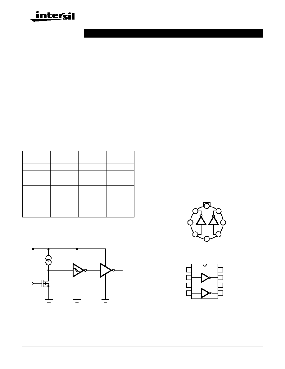
Functional Diagram
Features
∑ Fast Rise and Fall Times
- 30ns with 1000pF Load
∑ Wide Supply Voltage Range
- V
CC
= 4.5V to 15V
∑ Low Power Consumption
- 4mW with Inputs Low
- 20mW with Inputs High
∑ TTL/CMOS Input Compatible Power Driver
- R
OUT
= 7
Typ
∑ Direct Interface with Common PWM Control ICs
∑ Pin Equivalent to DS0026/DS0056; TSC426
Applications
∑ Switching Power Supplies
∑ DC/DC Converters
∑ Motor Controllers
Pinouts
ICL7667 (CAN)
TOP VIEW
ICL7667 (PDIP, SOIC, CERDIP)
TOP VIEW
Ordering Information
PART
NUMBER
TEMP. RANGE
(
o
C)
PACKAGE
PKG. NO.
ICL7667CBA
0 to 70
8 Ld SOIC (N)
M8.15
ICL7667CPA
0 to 70
8 Ld PDIP
E8.3
ICL7667CJA
0 to 70
8 Ld CERDIP
F8.3A
ICL7667CTV
0 to 70
8 Pin Metal Can T8.C
ICL7667MTV
(Note 1)
-55 to 125
8 Pin Metal Can T8.C
ICL7667MJA
(Note 1)
-55 to 125
8 Ld CERDIP
F8.3A
NOTE:
1. Add /883B to Part Number for 883B Processing
V
CC
IN
2mA
OUT
V+
N/C
N/C
V-
OUT A
IN A
OUT B
IN B
2
4
6
1
3
7
5
8
N/C
OUT A
V+
OUT B
N/C
IN A
V-
IN B
1
2
3
4
8
7
6
5
Data Sheet
April 1999
CAUTION: These devices are sensitive to electrostatic discharge; follow proper IC Handling Procedures.
http://www.intersil.com or 407-727-9207
|
Copyright
©
Intersil Corporation 1999
3-74
Absolute Maximum Ratings
Thermal Information
Supply Voltage V+ to V- . . . . . . . . . . . . . . . . . . . . . . . . . . . . . . . .15V
Input Voltage . . . . . . . . . . . . . . . . . . . . . . . . . . V- -0.3V to V+ +0.3V
Package Dissipation, T
A
25
o
C . . . . . . . . . . . . . . . . . . . . . . . .500mW
Operating Temperature Range
ICL7667C. . . . . . . . . . . . . . . . . . . . . . . . . . . . . . . . . . . . 0
o
C to 70
o
C
ICL7667M . . . . . . . . . . . . . . . . . . . . . . . . . . . . . . . . -55
o
C to 125
o
C
Thermal Resistance (Typical, Note 2)
JA
(
o
C/W)
JC
(
o
C/W)
PDIP Package . . . . . . . . . . . . . . . . . . .
150
N/A
SOIC Package . . . . . . . . . . . . . . . . . . .
170
N/A
Metal Can Package . . . . . . . . . . . . . . .
156
68
CERDIP Package . . . . . . . . . . . . . . . . .
115
30
Maximum Storage Temperature Range . . . . . . . . . . -65
o
C to 150
o
C
Maximum Lead Temperature (Soldering 10s) . . . . . . . . . . . . 300
o
C
(SOIC - Lead Tips Only)
CAUTION: Stresses above those listed in "Absolute Maximum Ratings" may cause permanent damage to the device. This is a stress only rating and operation of the
device at these or any other conditions above those indicated in the operational sections of this specification is not implied.
NOTE:
2.
JA
is measured with the component mounted on an evaluation PC board in free air.
Electrical Specifications
PARAMETER
SYMBOL
TEST CONDITIONS
ICL7667C, M
ICL7667M
UNITS
T
A
= 25
o
C
-55
o
C
T
A
125
o
C
MIN
TYP
MAX
MIN
TYP
MAX
DC SPECIFICATIONS
Logic 1 Input Voltage
V
IH
V
CC
= 4.5V
2.0
-
-
2.0
-
-
V
Logic 1 Input Voltage
V
IH
V
CC
= 15V
2.0
-
-
2.0
-
-
V
Logic 0 Input Voltage
V
IL
V
CC
= 4.5V
-
-
0.8
-
-
0.5
V
Logic 0 Input Voltage
V
IL
V
CC
= 15V
-
-
0.8
-
-
0.5
V
Input Current
I
IL
V
CC
= 15V, V
IN
= 0V and 15V
-0.1
-
0.1
-0.1
-
0.1
µ
A
Output Voltage High
V
OH
V
CC
= 4.5V and 15V
V
CC
-0.05
V
CC
-
V
CC
-0.1
V
CC
-
V
Output Voltage Low
V
OL
V
CC
= 4.5V and 15V
-
0
0.05
-
-
0.1
V
Output Resistance
R
OUT
V
IN
= V
IL
, I
OUT
= -10mA, V
CC
= 15V
-
7
10
-
-
12
Output Resistance
R
OUT
V
IN
= V
IH
, I
OUT
= 10mA, V
CC
= 15V
-
8
12
-
-
13
Power Supply Current
I
CC
V
CC
= 15V, V
IN
= 3V both inputs
-
5
7
-
-
8
mA
Power Supply Current
I
CC
V
CC
= 15V, V
IN
= 0V both inputs
-
150
400
-
-
400
µ
A
SWITCHING SPECIFICATIONS
Delay Time
T
D2
Figure 3
-
35
50
-
-
60
ns
Rise Time
T
R
Figure 3
-
20
30
-
-
40
ns
Fall Time
T
F
Figure 3
-
20
30
-
-
40
ns
Delay Time
T
D1
Figure 3
-
20
30
-
-
40
ns
NOTE: All typical values have been characterized but are not tested.
ICL7667
3-75
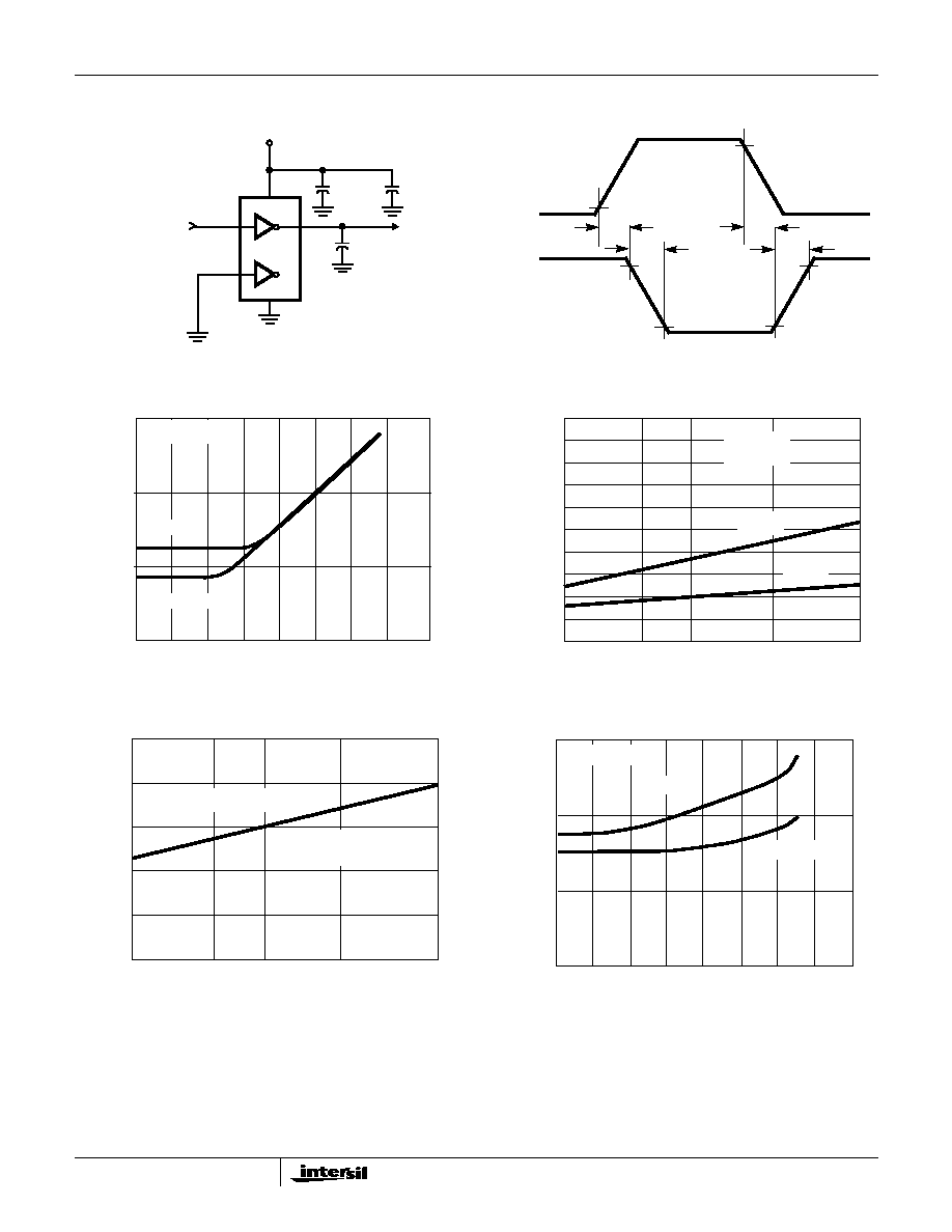
Test Circuits
ICL7667
INPUT
INPUT RISE AND
FALL TIMES
10ns
C
L
= 1000pF
4.7
µ
F
0.1
µ
F
+
OUTPUT
V- = 15V
90%
10%
10%
90%
10%
T
D1
t
f
90%
t
r
T
D2
0.4V
15V
INPUT
+5V
0V
OUTPUT
Typical Performance Curves
FIGURE 1. RISE AND FALL TIMES vs C
L
FIGURE 2. T
D1
, T
D2
vs TEMPERATURE
FIGURE 3. t
r
, t
f
vs TEMPERATURE
FIGURE 4. I
CC
vs C
L
t
RISE
t
FALL
10
100
1000
10K
100K
C
L
(pF)
t
r
AND t
f
, (ns)
1
µ
s
100
10
1
V
CC
= 15V
100
90
80
70
60
50
40
30
20
10
0
-55
0
25
70
125
TEMPERATURE (
o
C)
C
L
= 1nF
V
CC
= 15V
T
D2
T
D1
T
D1
AND T
D2
, (ns)
-55
0
25
70
125
50
40
30
20
10
0
TEMPERATURE (
o
C)
t
r
AND t
f
C
L
= 1nF
V
CC
= 15V
t
r
AND t
f
, (ns)
30
10
3.0
1
10
100
1K
10K
I
CC
(mA)
200kHz
20kHz
V
CC
= 15V
100K
C
L
(pF)
ICL7667

3-76
Detailed Description
The ICL7667 is a dual high-power CMOS inverter whose
inputs respond to TTL levels while the outputs can swing as
high as 15V. Its high output current enables it to rapidly
charge and discharge the gate capacitance of power
MOSFETs, minimizing the switching losses in switchmode
power supplies. Since the output stage is CMOS, the output
will swing to within millivolts of both ground and V
CC
without
any external parts or extra power supplies as required by the
DS0026/56 family. Although most specifications are at V
CC
=
15V, the propagation delays and specifications are almost
independent of V
CC
.
In addition to power MOS drivers, the ICL7667 is well suited
for other applications such as bus, control signal, and clock
drivers on large memory of microprocessor boards, where
the load capacitance is large and low propagation delays are
required. Other potential applications include peripheral
power drivers and charge-pump voltage inverters.
Input Stage
The input stage is a large N-Channel FET with a P-channel
constant-current source. This circuit has a threshold of about
1.5V, relatively independent of the VCC voltage. This means
that the inputs will be directly compatible with TTL over the
entire 4.5V - 15V V
CC
range. Being CMOS, the inputs draw
less than 1
µ
A of current over the entire input voltage range
of ground to V
CC
. The quiescent current or no load supply
current of the ICL7667 is affected by the input voltage, going
to nearly zero when the inputs are at the 0 logic level and
rising to 7mA maximum when both inputs are at the 1 logic
level. A small amount of hysteresis, about 50mV to 100mV at
the input, is generated by positive feedback around the
second stage.
Output Stage
The ICL7667 output is a high-power CMOS inverter,
swinging between ground and VCC. At V
CC
= 15V, the
output impedance of the inverter is typically 7
. The high
FIGURE 5. I
CC
vs FREQUENCY
FIGURE 6. NO LOAD I
CC
vs FREQUENCY
FIGURE 7. DELAY AND FALL TIMES vs V
CC
FIGURE 8. RISE TIME vs V
CC
Typical Performance Curves
(Continued)
FREQUENCY (Hz)
I
CC
(mA)
V
CC
= 15V
V
CC
= 5V
C
L
= 1nF
100
10
1
100
µ
A
10K
100K
1M
10M
100
10
1
100mA
10k
100k
1M
10M
V
CC
= 15V
V
CC
= 5V
C
L
= 10pF
FREQUENCY (Hz)
I
CC
(mA)
t
f
t
D1
V
CC
(V)
C
L
= 1nF
t
D1
AND t
f
, (ns)
50
40
30
20
10
0
5
10
15
V
CC
(V)
t
r
= T
D2
C
L
= 10pF
50
40
30
20
10
0
5
10
15
t
r
AND t
D2
, (ns)
ICL7667

3-77
peak current capability of the ICL7667 enables it to drive a
1000pF load with a rise time of only 40ns. Because the
output stage impedance is very low, up to 300mA will flow
through the series N-Channel and P-channel output devices
(from V
CC
to ground) during output transitions. This crossover
current is responsible for a significant portion of the internal
power dissipation of the ICL7667 at high frequencies. It can be
minimized by keeping the rise and fall times of the input to the
ICL7667 below 1
µ
s.
Application Notes
Although the ICL7667 is simply a dual level-shifting inverter,
there are several areas to which careful attention must be
paid.
Grounding
Since the input and the high current output current paths
both include the ground pin, it is very important to minimize
and common impedance in the ground return. Since the
ICL7667 is an inverter, any common impedance will
generate negative feedback, and will degrade the delay, rise
and fall times. Use a ground plane if possible, or use
separate ground returns for the input and output circuits. To
minimize any common inductance in the ground return,
separate the input and output circuit ground returns as close
to the ICL7667 as is possible.
Bypassing
The rapid charging and discharging of the load capacitance
requires very high current spikes from the power supplies. A
parallel combination of capacitors that has a low impedance
over a wide frequency range should be used. A 4.7
µ
F
tantalum capacitor in parallel with a low inductance 0.1
µ
F
capacitor is usually sufficient bypassing.
Output Damping
Ringing is a common problem in any circuit with very fast
rise or fall times. Such ringing will be aggravated by long
inductive lines with capacitive loads. Techniques to reduce
ringing include:
1. Reduce inductance by making printed circuit board traces
as short as possible.
2. Reduce inductance by using a ground plane or by closely
coupling the output lines to their return paths.
3. Use a 10
to 30
resistor in series with the output of the
ICL7667. Although this reduces ringing, it will also slightly
increase the rise and fall times.
4. Use good bypassing techniques to prevent supply voltage
ringing.
Power Dissipation
The power dissipation of the ICL7667 has three main
components:
5. Input inverter current loss
6. Output stage crossover current loss
7. Output stage I
2
R power loss
The sum of the above must stay within the specified limits for
reliable operation.
As noted above, the input inverter current is input voltage
dependent, with an I
CC
of 0.1mA maximum with a logic 0
input and 6mA maximum with a logic 1 input.
The output stage crowbar current is the current that flows
through the series N-Channel and P-channel devices that
form the output. This current, about 300mA, occurs only
during output transitions. Caution: The inputs should never
be allowed to remain between V
IL
and V
IH
since this could
leave the output stage in a high current mode, rapidly
leading to destruction of the device. If only one of the drivers
is being used, be sure to tie the unused input to a ground.
NEVER leave an input floating. The average supply current
drawn by the output stage is frequency dependent, as can
be seen in I
CC
vs Frequency graph in the Typical
Characteristics Graphs.
The output stage I
2
R power dissipation is nothing more than
the product of the output current times the voltage drop
across the output device. In addition to the current drawn by
any resistive load, there will be an output current due to the
charging and discharging of the load capacitance. In most
high frequency circuits the current used to charge and
discharge capacitance dominates, and the power dissipation
is approximately
P
AC
= CV
CC
2
f
where C = Load Capacitance, f = Frequency
In cases where the load is a power MOSFET and the gate
drive requirement are described in terms of gate charge, the
ICL7667 power dissipation will be
P
AC
= Q
G
V
CC
f
where Q
G
= Charge required to switch the gate, in
Coulombs, f = Frequency.
Power MOS Driver Circuits
Power MOS Driver Requirements
Because it has a very high peak current output, the ICL7667
the at driving the gate of power MOS devices. The high
current output is important since it minimizes the time the
power MOS device is in the linear region. Figure 9 is a
typical curve of charge vs gate voltage for a power MOSFET.
The flat region is caused by the Miller capacitance, where
the drain-to-gate capacitance is multiplied by the voltage
gain of the FET. This increase in capacitance occurs while
the power MOSFET is in the linear region and is dissipating
significant amounts of power. The very high current output of
the ICL7667 is able to rapidly overcome this high
capacitance and quickly turns the MOSFET fully on or off.
ICL7667