 | –≠–ª–µ–∫—Ç—Ä–æ–Ω–Ω—ã–π –∫–æ–º–ø–æ–Ω–µ–Ω—Ç: ICL8013 | –°–∫–∞—á–∞—Ç—å:  PDF PDF  ZIP ZIP |

1
File Number
2863.4
CAUTION: These devices are sensitive to electrostatic discharge; follow proper IC Handling Procedures.
1-888-INTERSIL or 321-724-7143
|
Copyright
©
Intersil Corporation 1999
ICL8013
1MHz, Four Quadrant Analog Multiplier
The ICL8013 is a four quadrant analog multiplier whose
output is proportional to the algebraic product of two input
signals. Feedback around an internal op amp provides level
shifting and can be used to generate division and square
root functions. A simple arrangement of potentiometers may
be used to trim gain accuracy, offset voltage and
feedthrough performance. The high accuracy, wide
bandwidth, and increased versatility of the ICL8013 make it
ideal for all multiplier applications in control and
instrumentation systems. Applications include RMS
measuring equipment, frequency doublers, balanced
modulators and demodulators, function generators, and
voltage controlled amplifiers.
Features
∑ Accuracy. . . . . . . . . . . . . . . . . . . . . . . .
±
1% ("B" Version)
∑ Input Voltage Range . . . . . . . . . . . . . . . . . . . . . . . . .
±
10V
∑ Bandwidth. . . . . . . . . . . . . . . . . . . . . . . . . . . . . . . . . 1MHz
∑ Uses Standard
±
15V Supplies
∑ Built-In Op Amp Provides Level Shifting, Division and
Square Root Functions
Pinout
ICL8013
(METAL CAN)
TOP VIEW
Functional Diagram
Ordering Information
PART
NUMBER
MULTIPLI-
CATION
ERROR
(MAX)
TEMP.
RANGE (
o
C)
PKG
PKG.
NO.
ICL8013BCTX
±
1%
0 to 70
10 Pin
Metal Can
T10.B
ICL8013CCTX
±
2%
0 to 70
10 Pin
Metal Can
T10.B
Y
OS
GND
V-
OUTPUT
V+
2
5
1
3
10
4
8
9
7
6
Z
OS
X
OS
X
IN
Z
IN
Y
IN
VOLTAGE TO CURRENT
CONVERTER AND
SIGNAL COMPRESSION
BALANCED
VARIABLE GAIN
AMPLIFIER
OP
AMP
OUT
VOLTAGE TO CURRENT
CONVERTER
Z
OS
Z
IN
Y
OS
Y
IN
X
IN
X
OS
Z
IN
Data Sheet
April 1999

2
Absolute Maximum Ratings
Thermal Information
Supply Voltage . . . . . . . . . . . . . . . . . . . . . . . . . . . . . . . . . . . . . .
±
18
Input Voltages (X
IN
, Y
IN
, Z
IN
, X
OS
, Y
OS
, Z
OS
) . . . . . . . . . V
SUPPLY
Operating Conditions
Temperature Range
ICL8013XC. . . . . . . . . . . . . . . . . . . . . . . . . . . . . . . . 0
o
C to 70
o
C
Thermal Resistance (Typical, Note 1)
JA
(
o
C/W)
JC
(
o
C/W)
Metal Can Package . . . . . . . . . . . . . . .
160
75
Maximum Junction Temperature (Metal Can Package) . . . . . . .175
o
C
Maximum Storage Temperature Range . . . . . . . . . . -65
o
C to 150
o
C
Maximum Lead Temperature (Soldering 10s) . . . . . . . . . . . . 300
o
C
CAUTION: Stresses above those listed in "Absolute Maximum Ratings" may cause permanent damage to the device. This is a stress only rating and operation of the
device at these or any other conditions above those indicated in the operational sections of this specification is not implied.
NOTE:
1.
JA
is measured with the component mounted on an evaluation PC board in free air.
Electrical Specifications
T
A
= 25
o
C, V
SUPPLY
=
±
15V, Gain and Offset Potentiometers Externally Trimmed, Unless Otherwise
Specified
PARAMETER
TEST
CONDITIONS
ICL8013B
ICL8013C
UNITS
MIN
TYP
MAX
MIN
TYP
MAX
Multiplier Function
-
XY
10
-
-
XY
10
-
Multiplication Error
-10 < X < 10
-10 < Y < 10
-
-
1.0
-
-
2.0
% Full Scale
Divider Function
-
10Z
X
-
-
10Z
X
-
Division Error
X = -10
-
0.3
-
-
0.3
-
% Full Scale
X = -1
-
1.5
-
-
1.5
-
% Full Scale
Feedthrough
X = 0, Y =
±
10V
-
-
100
-
-
200
mV
Y = 0, X =
±
10V
-
-
100
-
-
150
mV
Non-Linearity
X Input
X = 20V
P-P
Y=
±
10V
DC
-
±
0.5
-
-
±
0.8
-
%
Y Input
Y = 20V
P-P
X =
±
10V
DC
-
±
0.2
-
-
±
0.3
-
%
Frequency Response Small Signal
Bandwidth (-3dB)
-
1.0
-
-
1.0
-
MHz
Full Power Bandwidth
-
750
-
-
750
-
kHz
Slew Rate
-
45
-
-
45
-
V/
µ
s
1% Amplitude Error
-
75
-
-
75
-
kHz
1% Vector Error (0.5
o
Phase Shift)
-
5
-
-
5
-
kHz
Settling Time (to
±
2% of Final Value)
V
lN
=
±
10V
-
1
-
-
1
-
µ
s
Overload Recovery (to
±
2% of Final Value) V
lN
=
±
10V
-
1
-
-
1
-
µ
s
Output Noise
5Hz to 10kHz
-
0.6
-
-
0.6
-
mV
RMS
5Hz to 5MHz
-
3
-
-
3
-
mV
RMS
Input Resistance
V
lN
= 0V
X lnput
-
10
-
-
10
-
M
Y lnput
-
6
-
-
6
-
M
Z lnput
-
36
-
-
36
-
k
Input Bias Current
V
lN
= 0V
X or Y Input
-
-
7.5
-
-
10
µ
A
Z Input
-
25
-
-
25
-
µ
A
ICL8013
3
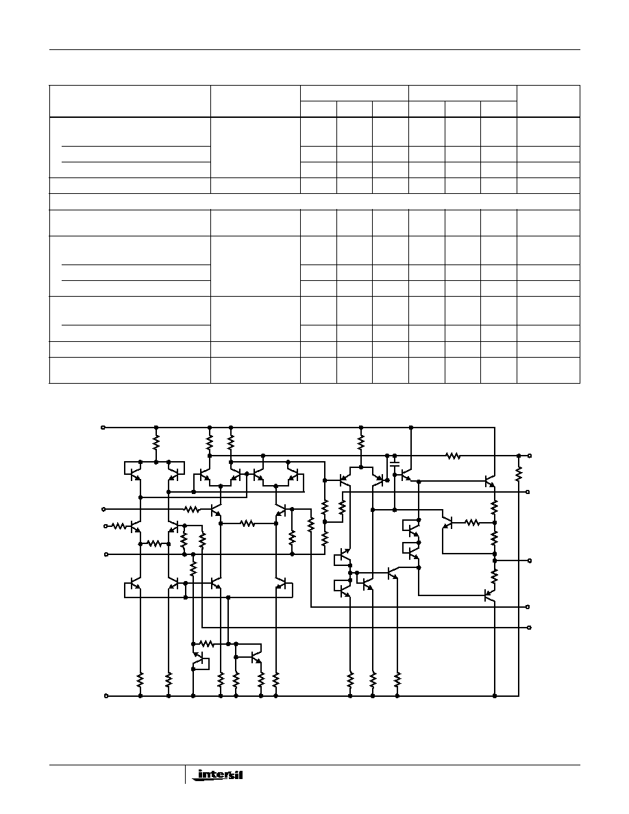
Schematic Diagram
Power Supply Variation
Multiplication Error
-
0.2
-
-
0.2
-
%/%
Output Offset
-
-
75
-
-
100
mV/V
Scale Factor
-
0.1
-
-
0.1
-
%/%
Quiescent Current
-
3.5
6.0
-
3.5
6.0
mA
THE FOLLOWING SPECIFICATIONS APPLY OVER THE OPERATING TEMPERATURE RANGES
Multiplication Error
-10V < X
IN
< 10V,
-10V < Y
IN
< 10V
-
2
-
-
3
-
% Full Scale
Average Temp. Coefficients
Accuracy
-
0.06
-
-
0.06
-
%/
o
C
Output Offset
-
0.2
-
-
0.2
-
mV/
o
C
Scale Factor
-
0.04
-
-
0.04
-
%/
o
C
Input Bias Current
V
IN
= 0V
X or Y Input
-
-
5
-
-
10
µ
A
Z Input
-
-
25
-
-
35
µ
A
Input Voltage (X, Y, or Z)
-
-
±
10
-
-
±
10
V
Output Voltage Swing
R
L
2k
C
L
< 1000pF
-
±
10
-
-
±
10
-
V
Electrical Specifications
T
A
= 25
o
C, V
SUPPLY
=
±
15V, Gain and Offset Potentiometers Externally Trimmed, Unless Otherwise Specified
(Continued)
PARAMETER
TEST
CONDITIONS
ICL8013B
ICL8013C
UNITS
MIN
TYP
MAX
MIN
TYP
MAX
Q
1
Q
2
Q
3
Q
4
R
3
R
1
COMMON
Y
IN
X
IN
V+
V-
Q
5
Q
6
R
4
R
5
Q
28
Q
7
Q
8
Q
14
Q
15
Q
10
R
13
Q
9
R
9
R
6
R
7
R
10
Q
11
Q
12
Q
13
R
12
R
15
R
11
R
19
R
18
R
17
Y
OS
X
OS
R
20
R
22
R
16
R
2
R
8
R
23
R
24
R
25
R
26
R
21
Q
19
Q
18
Q
20
Q
16
Q
24
Q
23
Q
22
Q
26
C
1
Q
21
R
27
Q
25
R
31
R
30
R
28
R
29
Q
27
R
33
OUTPUT
Z
IN
Q
17
R
32
Z
OS
ICL8013

4
Application Information
Detailed Circuit Description
The fundamental element of the ICL8013 multiplier is the
bipolar differential amplifier of Figure 1.
The small signal differential voltage gain of this circuit is
given by:
The output voltage is thus proportional to the product of the
input voltage V
lN
and the emitter current I
E
. In the simple
transconductance multiplier of Figure 2, a current source
comprising Q
3
, D
1
, and R
Y
is used. If V
Y
is large compared
with the drop across D
1
, then
There are several difficulties with this simple modulator:
1. V
Y
must be positive and greater than V
D
.
2. Some portion of the signal at V
X
will appear at the output
unless I
E
= 0.
3. V
X
must be a small signal for the differential pair to be
linear.
4. The output voltage is not centered around ground.
The first problem relates to the method of converting the V
Y
voltage to a current to vary the gain of the V
X
differential pair.
A better method, Figure 3, uses another differential pair but
with considerable emitter degeneration. In this circuit the
differential input voltage appears across the common emitter
resistor, producing a current which adds or subtracts from
the quiescent current in either collector. This type of voltage
to current converter handles signals from 0V to
±
10V with
excellent linearity.
The second problem is called feedthrough; i.e., the product
of zero and some finite Input signal does not produce zero
output voltage. The circuit whose operation is illustrated by
Figures 4A, 4B, and 4C overcomes this problem and forms
the heart of many multiplier circuits in use today.
This circuit is basically two matched differential pairs with
cross coupled collectors. Consider the case shown in Figure
4A of exactly equal current sources basing the two pairs.
With a small positive signal at V
lN
, the collector current of Q
1
and Q
4
will increase but the collector currents of Q
2
and Q
3
will decrease by the same amount. Since the collectors are
cross coupled the current through the load resistors remains
unchanged and independent of the V
lN
input voltage.
In Figure 4B, notice that with V
IN
= 0 any variation in the ratio
of biasing current sources will produce a common mode
voltage across the load resistors. The differential output
voltage will remain zero. In Figure 4C we apply a differential
input voltage with unbalanced current sources. If I
E1
is twice
I
E2
the gain of differential pair Q
1
and Q
2
is twice the gain of
pair Q
3
and Q
4
. Therefore, the change in cross coupled
collector currents will be unequal and a differential output
voltage will result. By replacing the separate biasing current
sources with the voltage to current converter of Figure 3 we
have a balanced multiplier circuit capable of four quadrant
operation (Figure 5).
2I
E
R
L
R
L
V
IN
V
OUT
V+
V-
FIGURE 1. DIFFERENTIAL AMPLIFIER
A
V
V
OUT
V
IN
----------------
R
L
r
E
-------
=
=
Substituting r
E
1
g
M
-------
kT
qI
E
---------
=
=
V
OUT
V
IN
R
L
r
E
-------
V
IN
qI
E
R
L
kT
-------------------
◊
=
=
I
D
V
Y
R
Y
--------
2I
E
and
=
V
OUT
qR
L
kTR
Y
---------------
V
X
V
Y
◊
(
)
=
2I
E
R
L
R
L
V
IN
V
OUT
V+
V-
Q
3
R
Y
V
Y
I
D
V
D
D
1
qR
L
kTR
Y
(V
X
x V
Y
)
V
OUT
= K (V
X
x V
Y
) =
-
+
FIGURE 2. TRANSCONDUCTANCE MULTIPLIER
I
E
+
I
I
E
I
E
-
I
V
IN
V
OUT
V+
V-
I
E
I =
V
IN
R
E
FIGURE 3. VOLTAGE TO CURRENT CONVERTER
ICL8013

5
This circuit of Figure 5 still has the problem that the input
voltage V
IN
must be small to keep the differential amplifier in
the linear region. To be able to handle large signals, we need
an amplitude compression circuit.
Figure 2 showed a current source formed by relying on the
matching characteristics of a diode and the emitter base
junction of a transistor. Extension of this idea to a differential
circuit is shown in Figure 6A. In a differential pair, the input
voltage splits the biasing current in a logarithmic ratio. (The
usual assumption of linearity is useful only for small signals.)
Since the input to the differential pair in Figure 6A is the
difference in voltage across the two diodes, which in turn is
proportional to the log of the ratio of drive currents, it follows
that the ratio of diode currents and the ratio of collector
currents are linearly related and independent of amplitude. If
we combine this circuit with the voltage to current converter
of Figure 3, we have Figure 6B. The output of the differential
amplifier is now proportional to the input voltage over a large
dynamic range, thereby improving linearity while minimizing
drift and noise factors.
The complete schematic is shown after the Electrical
Specifications Table. The differential pair Q
3
and Q
4
form a
voltage to current converter whose output is compressed in
collector diodes Q
1
and Q
2
. These diodes drive the
balanced cross-coupled differential amplifier Q
7
/Q
8
Q
14
/Q
15
.
The gain of these amplifiers is modulated by the voltage to
current converter Q
9
and Q
10
. Transistors Q
5
, Q
6
, Q
11
, and
Q
12
are constant current sources which bias the voltage to
current converter. The output amplifier comprises transistors
Q
16
through Q
27
.
I
E
R
L
V
IN
V
OUT
= 0
V+
I
E
V-
1
/
2
I
E
+
+
-
1
/
2
I
E
-
R
L
Q
1
Q
2
Q
3
Q
4
1
/
2
I
E
-
1
/
2
I
E
+
I
E
I
E
FIGURE 4A. INPUT SIGNAL WITH BALANCED CURRENT
SOURCES
V
OUT
= 0V
I
E
R
L
V
IN
= 0
V
OUT
= 0
V+
2I
E
V-
1
/
2
I
E
+
-
1
/
2
I
E
R
L
Q
1
Q
2
Q
3
Q
4
I
E
I
E
FIGURE 4B. NO INPUT SIGNAL WITH UNBALANCED
CURRENT SOURCES
V
OUT
= 0V
I
E
R
L
V
IN
V
OUT
= 0
V+
2I
E
V-
1
/
2
I
E
+
+
-
1
/
2
I
E
-
R
L
Q
1
Q
2
Q
3
Q
4
1
/
2
I
E
- 2
I
E
+ 2
3
/
2
I +
3
/
2
I -
FIGURE 4C. INPUT SIGNAL WITH UNBALANCED CURRENT
SOURCES, DIFFERENTIAL OUTPUT VOLTAGE
I
E
R
L
V
IN
V = K ∑ (V
X
∑ V
Y
)
V+
I
E
V-
+
-
R
Q
1
Q
2
Q
3
Q
4
R
E
V
IN
FIGURE 5. TYPICAL FOUR QUADRANT MULTIPLIER-
MODULATOR
X x I
D
X x I
E
(I - X) I
E
(I - X) I
D
2 I
E
FIGURE 6A. CURRENT GAIN CELL
ICL8013

6
Definition of Terms
Multiplication/Division Error: This is the basic accuracy
specification. It includes terms due to linearity, gain, and
offset errors, and is expressed as a percentage of the full
scale output.
Feedthrough: With either input at zero, the output of an
ideal multiplier should be zero regardless of the signal
applied to the other input. The output seen in a non-ideal
multiplier is known as the feedthrough.
Nonlinearity: The maximum deviation from the best
straight line constructed through the output data, expressed
as a percentage of full scale. One input is held constant and
the other swept through it nominal range. The nonlinearity is
the component of the total multiplication/division error which
cannot be trimmed out.
Typical Applications
Multiplication
In the standard multiplier connection, the Z terminal is
connected to the op amp output. All of the modulator output
current thus flows through the feedback resistor R
27
and
produces a proportional output voltage.
MULTIPLIER TRIMMING PROCEDURE
1. Set X
IN
= Y
IN
= 0V and adjust Z
OS
for zero Output.
2. Apply a
±
10V low frequency (
100Hz) sweep (sine or trian-
gle) to Y
IN
with X
IN
= 0V, and adjust X
OS
for minimum out-
put.
3. Apply the sweep signal of Step 2 to X
IN
with Y
IN
= 0V and
adjust Y
OS
for minimum Output.
4. Readjust Z
OS
as in Step 1, if necessary.
5. With X
IN
= 10.0V
DC
and the sweep signal of Step 2 applied
to Y
IN
, adjust the Gain potentiometer for Output = Y
IN
.
This is easily accomplished with a differential scope plug-
in (A+B) by inverting one signal and adjusting Gain control
for (Output - Y
IN
) = Zero.
Division
If the Z terminal is used as an input, and the output of the op
amp connected to the Y input, the device functions as a
divider. Since the input to the op amp is at virtual ground,
and requires negligible bias current, the overall feedback
forces the modulator output current to equal the current
produced by Z.
Note that when connected as a divider, the X input must be a
negative voltage to maintain overall negative feedback.
DIVIDER TRIMMING PROCEDURE
1. Set trimming potentiometers at mid-scale by adjusting
voltage on pins 7, 9 and 10 (X
OS
, Y
OS
, Z
OS
) for 0V.
2. With Z
IN
= 0V, trim Z
OS
to hold the Output constant, as
X
IN
is varied from -10V through -1V.
3. With Z
IN
= 0V and X
IN
= -10.0V adjust Y
OS
for zero Out-
put voltage.
4. With Z
IN
= X
IN
(and/or Z
IN
= -X
IN
) adjust X
OS
for mini-
mum worst case variation of Output, as X
IN
is varied from
-10V to -1V.
5. Repeat Steps 2 and 3 if Step 4 required a large initial ad-
justment.
6. With Z
IN
= X
IN
(and/or Z
IN
= -X
IN
) adjust the gain control
until the output is the closest average around +10.0V
(-10V for Z
IN
= -X
IN
) as X
IN
is varied from -10V to -3V.
V
IN
V+
V
OUT
V-
V-
FIGURE 6B. VOLTAGE GAIN WITH SIGNAL COMPRESSION
OP AMP
MODULATOR
X
IN
Y
IN
Z
IN
I
O
= X
IN
∑ Y
IN
R =
V
OUT
=
1
10
X
IN
Y
IN
10
FIGURE 7A. MULTIPLIER BLOCK DIAGRAM
ICL8013
Z
IN
X
IN
Y
IN
5K
7.5K
7
10
9
X
OS
Y
OS
Z
OS
4
3
6
1
OUTPUT =
X
IN
Y
IN
10
FIGURE 7B. MULTIPLIER CIRCUIT CONNECTION
Therefore I
O
X
IN
Y
IN
∑
Z
IN
R
----------
10Z
IN
=
=
=
Since Y
IN
V
OUT
V
OUT
,
10Z
IN
X
IN
-----------------
=
=
ICL8013

7
Squaring
The squaring function is achieved by simply multiplying with
the two inputs tied together. The squaring circuit may also be
used as the basis for a frequency doubler since cos
2
t =
1
/
2
(cos 2
t + 1).
Square Root
Tying the X and Y inputs together and using overall feedback
from the op amp results in the square root function. The
output of the modulator is again forced to equal the current
produced by the Z input.
The output is a negative voltage which maintains overall
negative feedback. A diode in series with the op amp output
prevents the latchup that would otherwise occur for negative
input voltages.
SQUARE ROOT TRIMMING PROCEDURE
1. Connect the ICL8013 in the Divider configuration.
2. Adjust Z
OS
, Y
OS
, X
OS
, and Gain using Steps 1 through 6
of Divider Trimming Procedure.
3. Convert to the Square Root configuration by connecting
X
IN
to the output and inserting a diode between Pin 4 and
the output node.
4. With Z
IN
= 0V adjust Z
OS
for zero output voltage.
Variable Gain Amplifier
Most applications for the ICL8013 are straight forward
variations of the simple arithmetic functions described
above. Although the circuit description frequently disguises
the fact, it has already been shown that the frequency
doubIer is nothing more than a squaring circuit. Similarly the
variable gain amplifier is nothing more than a multiplier, with
the input signal applied at the X input and the control voltage
applied at the Y input.
OP AMP
MODULATOR
X
IN
Y
IN
Z
IN
I
Z
R =
V
OUT
=
1
10
10Z
IN
X
IN
I
O
FIGURE 8A. DIVISION BLOCK DIAGRAM
ICL8013
Z
IN
X
IN
Y
IN
5K
7.5K
7
10
9
X
OS
Y
OS
Z
OS
4
6
3
1
OUTPUT =
10Z
IN
X
IN
GAIN
(0 TO -10V)
FIGURE 8B. DIVISION CIRCUIT CONNECTION
OP AMP
X
IN
Y
IN
Z
IN
I
O
= X
IN
∑ Y
IN
R =
V
OUT
=
1
10
X
IN
2
10
X
FIGURE 9A. SQUARER BLOCK DIAGRAM
ICL8013
X
IN
7.5k
7
10
9
X
OS
Y
OS
Z
OS
4
3
6
1
OUTPUT =
X
IN
2
10
5k
SCALE
FACTOR
ADJUST
FIGURE 9B. SQUARER CIRCUIT CONNECTION
I
O
X
IN
Y
IN
◊
V
OUT
≠
(
)
2
10Z
IN
=
=
=
V
OUT
10Z
IN
≠
=
OP AMP
MODULATOR
X
IN
Y
IN
Z
I
Z
R =
V
OUT
= -
10Z
IN
1
10
I
O
= V
O
2
FIGURE 10A. SQUARE ROOT BLOCK DIAGRAM
ICL8013
Z
IN
X
IN
Y
IN
5K
7.5K
7
10
9
X
OS
Y
OS
Z
OS
4
6
3
1
OUTPUT = -
10ZIN
GAIN
(0V TO + 10V)
1N4148
FIGURE 10B. ACTUAL CIRCUIT CONNECTION
ICL8013

8
All Intersil semiconductor products are manufactured, assembled and tested under ISO9000 quality systems certification.
Intersil semiconductor products are sold by description only. Intersil Corporation reserves the right to make changes in circuit design and/or specifications at any time with-
out notice. Accordingly, the reader is cautioned to verify that data sheets are current before placing orders. Information furnished by Intersil is believed to be accurate and
reliable. However, no responsibility is assumed by Intersil or its subsidiaries for its use; nor for any infringements of patents or other rights of third parties which may result
from its use. No license is granted by implication or otherwise under any patent or patent rights of Intersil or its subsidiaries.
For information regarding Intersil Corporation and its products, see web site http://www.intersil.com
ICL8013
Z
INPUT
GAIN
5K
7.5K
7
10
9
X
OS
Y
OS
Z
OS
4
3
6
1
OUTPUT =
XY
10
CONTROL
VOLTAGE
FIGURE 11. VARIABLE GAIN AMPLIFIER
X
OS
Y
OS
Z
OS
V+
V-
20K
20K
20K
FIGURE 12. POTENTIOMETERS FOR TRIMMING OFFSET AND
FEEDTHROUGH
Typical Performance Curves
FIGURE 13. FREQUENCY RESPONSE
FIGURE 14. NONLINEARITY vs FREQUENCY
FIGURE 15. FEEDTHROUGH vs FREQUENCY
AMPLITUDE (dB)
FREQUENCY (Hz)
PHASE (DEGREES)
PHASE
AMPLITUDE
1K
10K
100K
1M
10M
25
0
5
10
15
20
-50
0
-10
-20
-30
-40
FREQUENCY (Hz)
1K
10K
100K
100
100
10
1
0.1
0.01
NONLINEARITY (% OF FULL SCALE)
Y-INPUT
X-INPUT
FREQUENCY (Hz)
1K
10K
100K
1M
10M
FEEDTHR
OUGH (dB)
-10
-20
-30
-40
-50
-60
-70
X = 0, Y = 20V
P-P
Y = 0, X = 20V
P-P
ICL8013