ISL3170E, ISL3171E, ISL3172E, ISL3173E, ISL3174E, ISL3175E, ISL3176E, ISL3177E, ISL3178E
1
®
FN6307.2
ISL3170E, ISL3171E, ISL3172E, ISL3173E, ISL3174E,
ISL3175E, ISL3176E, ISL3177E
,
ISL3178E
±
15kV ESD Protected, 3.3V, Full Fail-safe,
Low Power, High Speed or Slew Rate
Limited, RS-485/RS-422 Transceivers
The Intersil ISL317XE are
±
15kV
IEC61000
ESD Protected,
3.3V powered, single transceivers that meet both the
RS-485 and RS-422 standards for balanced communication.
These devices have very low bus currents (+125
A/-100
A),
so they present a true "1/8 unit load" to the RS-485 bus. This
allows up to 256 transceivers on the network without violating
the RS-485 specification's 32 unit load maximum, and without
using repeaters. For example, in a remote utility meter reading
system, individual meter readings are routed to a concentrator
via an RS-485 network, so the high allowed node count
minimizes the number of repeaters required.
Receiver (Rx) inputs feature a "Full Fail-Safe" design, which
ensures a logic high Rx output if Rx inputs are floating,
shorted, or terminated but undriven.
Hot Plug circuitry ensures that the Tx and Rx outputs remain
in a high impedance state while the power supply stabilizes.
The ISL3170E through ISL3175E utilize slew rate limited
drivers which reduce EMI, and minimize reflections from
improperly terminated transmission lines, or unterminated
stubs in multidrop and multipoint applications. Slew rate limited
versions also include receiver input filtering to enhance noise
immunity in the presence of slow input signals.
The ISL3170E, ISL3171E, ISL3173E, ISL3174E, ISL3176E
,
ISL3177E
are configured for full duplex (separate Rx input
and Tx output pins) applications. The half duplex versions
multiplex the Rx inputs and Tx outputs to allow transceivers
with output disable functions in 8 lead packages.
Features
·
IEC61000
ESD Protection on RS-485 I/O Pins
. . . . . ±
15kV
- Class 3 ESD Level on all Other Pins . . . . . . >7kV HBM
· Pb-Free Plus Anneal Available (RoHS Compliant)
· Full Fail-safe (Open, Short, Terminated/Floating)
Receivers
· Hot Plug - Tx and Rx Outputs Remain Three-state During
Power-up
· True 1/8 Unit Load Allows up to 256 Devices on the Bus
· Single 3.3V Supply
· High Data Rates. . . . . . . . . . . . . . . . . . . . . . up to 20Mbps
· Low Quiescent Supply Current . . . . . . . . . . .800
A (Max)
- Ultra Low Shutdown Supply Current . . . . . . . . . . .10nA
· -7V to +12V Common Mode Input/Output Voltage Range
· Half and Full Duplex Pinouts
· Three State Rx and Tx Outputs Available
· Current Limiting and Thermal Shutdown for driver
Overload Protection
· Tiny MSOP Packages Consume 50% Less Board Space
Applications
· Automated Utility Meter Reading Systems
· High Node Count Systems
· Field Bus Networks
· Security Camera Networks
· Building Environmental Control/ Lighting Systems
· Industrial/Process Control Networks
TABLE 1. SUMMARY OF FEATURES
PART
NUMBER
HALF/FULL
DUPLEX
DATA RATE
(Mbps)
SLEW-RATE
LIMITED?
HOT
PLUG?
# DEVICES
ON BUS
RX/TX
ENABLE?
QUIESCENT
I
CC
(
A)
LOW POWER
SHUTDOWN?
PIN
COUNT
ISL3170E
FULL
0.25
YES
YES
256
YES
510
YES
10, 14
ISL3171E
FULL
0.25
YES
YES
256
NO
510
NO
8
ISL3172E
HALF
0.25
YES
YES
256
YES
510
YES
8
ISL3173E
FULL
0.5
YES
YES
256
YES
510
YES
10, 14
ISL3174E
FULL
0.5
YES
YES
256
NO
510
NO
8
ISL3175E
HALF
0.5
YES
YES
256
YES
510
YES
8
ISL3176E
FULL
20
NO
YES
256
YES
510
YES
10, 14
ISL3177E
FULL
20
NO
YES
256
NO
510
NO
8
ISL3178E
HALF
20
NO
YES
256
YES
510
YES
8
Data Sheet
August 28, 2006
CAUTION: These devices are sensitive to electrostatic discharge; follow proper IC Handling Procedures.
1-888-INTERSIL or 1-888-468-3774
|
Intersil (and design) is a registered trademark of Intersil Americas Inc.
Copyright Intersil Americas Inc. 2006. All Rights Reserved
All other trademarks mentioned are the property of their respective owners.
2
FN6307.2
August 28, 2006
Pinouts
ISL3172E, ISL3175E, ISL3178E
(MSOP, SOIC)
TOP VIEW
ISL3171E, ISL3174E, ISL3177E
(MSOP, SOIC)
TOP VIEW
ISL3170E, ISL3173E, ISL3176E
(MSOP)
TOP VIEW
ISL3170E, ISL3173E, ISL3176E
(SOIC)
TOP VIEW
RO
RE
DE
DI
1
2
3
4
8
7
6
5
V
CC
B/Z
A/Y
GND
D
R
V
CC
RO
DI
GND
1
2
3
4
8
7
6
5
A
B
Z
Y
D
R
RO
RE
DE
DI
GND
V
CC
A
B
Z
Y
1
2
3
4
5
10
9
8
7
6
D
R
NC
RO
RE
DE
DI
GND
GND
V
CC
NC
A
B
Z
Y
NC
1
2
3
4
5
6
7
14
13
12
11
10
9
8
D
R
Ordering Information
(Notes 1, 2)
PART NUMBER
PART MARKING
TEMP. RANGE (°C)
PACKAGE (Pb-Free)
PKG. DWG. #
ISL3170EIBZ
3170EIBZ
-40 to +85
14 Ld SOIC
M14.15
ISL3170EIUZ
3170Z
-40 to +85
10 Ld MSOP
M10.118
ISL3171EIBZ
3171EIBZ
-40 to +85
8 Ld SOIC
M8.15
ISL3171EIUZ
3171Z
-40 to +85
8 Ld MSOP
M8.118
ISL3172EIBZ
3172EIBZ
-40 to +85
8 Ld SOIC
M8.15
ISL3172EIUZ
3172Z
-40 to +85
8 Ld MSOP
M8.118
ISL3173EIBZ
3173EIBZ
-40 to +85
14 Ld SOIC
M14.15
ISL3173EIUZ
3173Z
-40 to +85
10 Ld MSOP
M10.118
ISL3174EIBZ
3174EIBZ
-40 to +85
8 Ld SOIC
M8.15
ISL3174EIUZ
3174Z
-40 to +85
8 Ld MSOP
M8.118
ISL3175EIBZ
3175EIBZ
-40 to +85
8 Ld SOIC
M8.15
ISL3175EIUZ
3175Z
-40 to +85
8 Ld MSOP
M8.118
ISL3176EIBZ
3176EIBZ
-40 to +85
14 Ld SOIC
M14.15
ISL3176EIUZ
3176Z
-40 to +85
10 Ld MSOP
M10.118
ISL3177EIBZ
3177EIBZ
-40 to +85
8 Ld SOIC
M8.15
ISL3177EIUZ
3177Z
-40 to +85
8 Ld MSOP
M8.118
ISL3178EIBZ
3178EIBZ
-40 to +85
8 Ld SOIC
M8.15
ISL3178EIUZ
3178Z
-40 to +85
8 Ld MSOP
M8.118
NOTES:
1. Units also available in Tape and Reel; Add "-T" to suffix.
2. Intersil Pb-free plus anneal products employ special Pb-free material sets; molding compounds/die attach materials and 100% matte tin plate
termination finish, which are RoHS compliant and compatible with both SnPb and Pb-free soldering operations. Intersil Pb-free products are
MSL classified at Pb-free peak reflow temperatures that meet or exceed the Pb-free requirements of IPC/JEDEC J STD-020.
ISL3170E, ISL3171E, ISL3172E, ISL3173E, ISL3174E, ISL3175E, ISL3176E, ISL3177E, ISL3178E
3
FN6307.2
August 28, 2006
Truth Tables
TRANSMITTING
INPUTS
OUTPUTS
RE
DE
DI
Z
Y
X
1
1
0
1
X
1
0
1
0
0
0
X
High-Z
High-Z
1
0
X
High-Z *
High-Z *
NOTE: *Shutdown Mode (See Note 9), except for ISL3171E,
ISL3174E, ISL3177E
RECEIVING
INPUTS
OUTPUT
RE
DE
Half Duplex
DE
Full Duplex
A-B
RO
0
0
X
-0.05V
1
0
0
X
-0.2V
0
0
0
X
Inputs
Open/Shorted
1
1
0
0
X
High-Z *
1
1
1
X
High-Z
NOTE: *Shutdown Mode (See Note 9), except for ISL3171E,
ISL3174E, ISL3177E
Pin Descriptions
PIN
FUNCTION
RO
Receiver output: If A-B
-50mV, RO is high; If A-B
-200mV, RO is low; RO = High if A and B are unconnected (floating) or shorted.
RE
Receiver output enable. RO is enabled when RE is low; RO is high impedance when RE is high. If the Rx enable function isn't used,
connect RE directly to GND or through a 1k
to 3k
resistor to GND.
DE
Driver output enable. The driver outputs, Y and Z, are enabled by bringing DE high, and are high impedance when DE is low. If the
Tx enable function isn't used, connect DE to V
CC
through a 1k
to 3k
resistor.
DI
Driver input. A low on DI forces output Y low and output Z high. Similarly, a high on DI forces output Y high and output Z low.
GND
Ground connection.
A/Y
±
15kV IEC61000 ESD Protected RS-485/422 level, noninverting receiver input and noninverting driver output. Pin is an input if
DE = 0; pin is an output if DE = 1.
B/Z
±
15kV IEC61000 ESD Protected RS-485/422 level, Inverting receiver input and inverting driver output. Pin is an input if DE = 0;
pin is an output if DE = 1.
A
±
15kV
IEC61000
ESD Protected RS-485/422 level, noninverting receiver input.
B
±
15kV
IEC61000
ESD Protected RS-485/422 level, inverting receiver input.
Y
±
15kV
IEC61000
ESD Protected RS-485/422 level, noninverting driver output.
Z
±
15kV
IEC61000
ESD Protected RS-485/422 level, inverting driver output.
V
CC
System power supply input (3.0V to 3.6V).
NC
No Connection.
ISL3170E, ISL3171E, ISL3172E, ISL3173E, ISL3174E, ISL3175E, ISL3176E, ISL3177E, ISL3178E
4
FN6307.2
August 28, 2006
Typical Operating Circuits
ISL3172E, ISL3175E, ISL3178E
ISL3171E, ISL3174E, ISL3177E
ISL3170E, ISL3173E, ISL3176E
0.1
F
+
D
R
7
6
8
1
2
3
4
5
V
CC
GND
RO
RE
DE
DI
A/Y
B/Z
+3.3V
0.1
F
+
D
R
6
7
8
1
2
3
4
5
V
CC
GND
RO
RE
DE
DI
A/Y
B/Z
+3.3V
R
T
R
T
0.1
F
+
D
R
8
7
6
5
1
2
3
4
V
CC
GND
RO
DI
A
B
Y
Z
+3.3V
0.1
F
+
D
R
8
7
6
5
1
2
3
4
V
CC
GND
RO
DI
A
B
Y
Z
+3.3V
R
T
R
T
0.1
F
+
D
R
12
11
10
9
14
2
3
4
5
6, 7
V
CC
GND
RO
RE
DE
DI
A
B
Y
Z
+3.3V
0.1
F
+
D
R
12
11
10
9
14
2
3
4
5
6, 7
V
CC
GND
RO
RE
DE
DI
A
B
Y
Z
+3.3V3
R
T
R
T
(PIN NUMBERS FOR SOIC)
ISL3170E, ISL3171E, ISL3172E, ISL3173E, ISL3174E, ISL3175E, ISL3176E, ISL3177E, ISL3178E
5
FN6307.2
August 28, 2006
Absolute Maximum Ratings
Thermal Information
V
CC
to Ground. . . . . . . . . . . . . . . . . . . . . . . . . . . . . . . . . . . . . . . 7V
Input Voltages
DI, DE, RE . . . . . . . . . . . . . . . . . . . . . . . . . . . . . . . . . -0.3V to 7V
Input/Output Voltages
A, B, Y, Z . . . . . . . . . . . . . . . . . . . . . . . . . . . . . . . . . . -8V to +13V
RO . . . . . . . . . . . . . . . . . . . . . . . . . . . . . . . . -0.3V to (V
CC
+0.3V)
Short Circuit Duration
Y, Z . . . . . . . . . . . . . . . . . . . . . . . . . . . . . . . . . . . . . . . Continuous
ESD Rating . . . . . . . . . . . . . . . . . . . . . . . . . See Specification Table
Operating Conditions
Temperature Range . . . . . . . . . . . . . . . . . . . . . . . . . .-40°C to +85°C
Thermal Resistance (Typical, Note 3)
JA
(°C/W)
8 Ld SOIC Package . . . . . . . . . . . . . . . . . . . . . . . . .
+105
8 Ld MSOP Package . . . . . . . . . . . . . . . . . . . . . . . .
+140
10 Ld MSOP Package . . . . . . . . . . . . . . . . . . . . . . .
+190
14 Ld SOIC Package . . . . . . . . . . . . . . . . . . . . . . . .
+128
Maximum Junction Temperature (Plastic Package) . . . . . . +150°C
Maximum Storage Temperature Range . . . . . . . . . .-65°C to +150°C
Maximum Lead Temperature (Soldering 10s) . . . . . . . . . . . +300°C
(Lead Tips Only)
CAUTION: Stresses above those listed in "Absolute Maximum Ratings" may cause permanent damage to the device. This is a stress only rating and operation of the
device at these or any other conditions above those indicated in the operational sections of this specification is not implied.
NOTE:
3.
JA
is measured with the component mounted on a high effective thermal conductivity test board in free air. See Tech Brief TB379 for details.
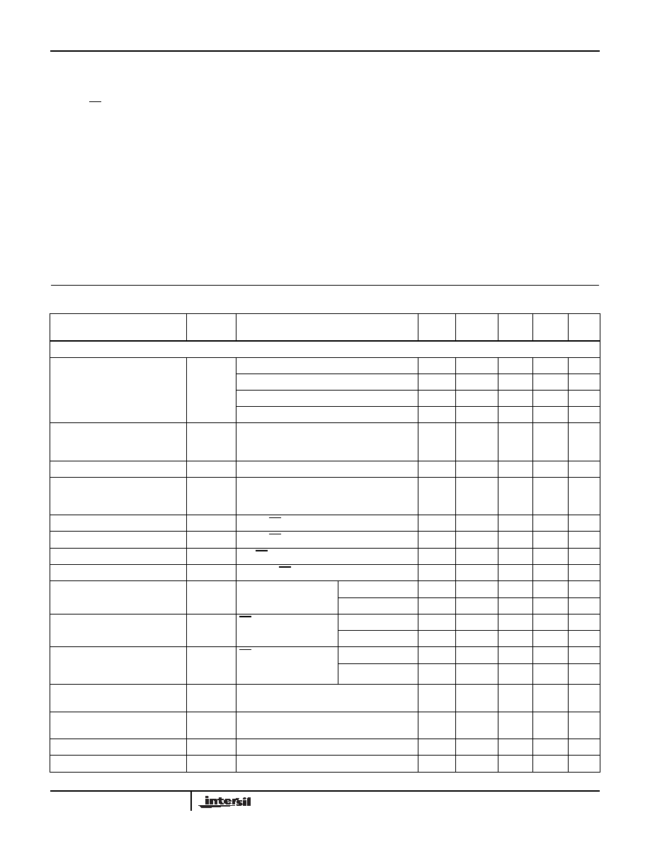
Electrical Specifications
Test Conditions: V
CC
= 3.0V to 3.6V; Unless Otherwise Specified. Typicals are at V
CC
= 3.3V, T
A
= +25
°C
,
Note 4
PARAMETER
SYMBOL
TEST CONDITIONS
TEMP
(°C)
MIN
TYP
MAX
UNITS
DC CHARACTERISTICS
Driver Differential V
OUT
V
OD
R
L
= 100
(RS-422) (Figure 1A, Note 15)
Full
2
2.3
-
V
R
L
= 54
(RS-485) (Figure 1A)
Full
1.5
2
V
CC
V
No Load
-
-
V
CC
R
L
= 60
, -7V
V
CM
12V (Figure 1B)
Full
1.5
2.2
-
V
Change in Magnitude of Driver
Differential V
OUT
for
Complementary Output States
V
OD
R
L
= 54
or 100
(Figure 1A)
Full
-
0.01
0.2
V
Driver Common-Mode V
OUT
V
OC
R
L
= 54
or 100
(Figure 1A)
Full
-
2
3
V
Change in Magnitude of Driver
Common-Mode V
OUT
for
Complementary Output States
V
OC
R
L
= 54
or 100
(Figure 1A)
Full
-
0.01
0.2
V
Logic Input High Voltage
V
IH
DI, DE, RE
Full
2
-
-
V
Logic Input Low Voltage
V
IL
DI, DE, RE
Full
-
-
0.8
V
Logic Input Hysteresis
V
HYS
DE, RE (Note 14)
25
-
100
-
mV
Logic Input Current
I
IN1
DI = DE = RE = 0V or V
CC
(Note 17)
Full
-2
-
2
A
Input Current (A, B, A/Y, B/Z)
I
IN2
DE = 0V, V
CC
= 0V or
3.6V
V
IN
= 12V
Full
-
80
125
A
V
IN
= -7V
Full
-100
-50
-
A
Output Leakage Current (Y, Z) (Full
Duplex Versions Only, Note 12)
I
IN3
RE = 0V, DE = 0V,
V
CC
= 0V or 3.6V
V
IN
= 12V
Full
-
10
40
A
V
IN
= -7V
Full
-40
-10
-
A
Output Leakage Current (Y, Z)
in Shutdown Mode (Full Duplex,
Note 12)
I
IN4
RE = V
CC
, DE = 0V,
V
CC
= 0V or 3.6V
V
IN
= 12V
Full
-
10
40
A
V
IN
= -7V
Full
-40
-10
-
A
Driver Short-Circuit Current,
V
O
= High or Low
I
OSD1
DE = V
CC
, -7V
V
Y
or V
Z
12V (Note 6)
Full
-
-
±
250
mA
Receiver Differential Threshold
Voltage
V
TH
-7V
V
CM
12V
Full
-200
-125
-50
mV
Receiver Input Hysteresis
V
TH
V
CM
= 0V
25
-
15
-
mV
Receiver Output High Voltage
V
OH
I
O
= -4mA, V
ID
= -50mV
Full
V
CC
- 0.6
-
-
V
ISL3170E, ISL3171E, ISL3172E, ISL3173E, ISL3174E, ISL3175E, ISL3176E, ISL3177E, ISL3178E