1
Æ
FN6032
ISL43140, ISL43141, ISL43142
Low-Voltage, Single and Dual Supply,
High Performance, Quad SPST, Analog
Switches
The Intersil ISL43140≠ISL43142 devices are CMOS,
precision, quad analog switches designed to operate from a
single +2V to +12V supply or from a
±
2V to
±
6V supply.
Targeted applications include battery powered equipment that
benefit from the devices' low power consumption (1
µ
W), low
leakage currents (1nA max), and fast switching speeds
(t
ON
= 30ns, t
OFF
= 18ns). A 12
maximum R
ON
flatness
ensures signal fidelity, while channel-to-channel mismatch is
guaranteed to be less than 2.5
. The 3mm x 3mm Quad No-
Lead Flatpack (QFN) package alleviates board space
limitations, making this newest line of low-voltage switches an
ideal solution.
The ISL43140/ISL43141/ISL43142 are quad single-pole/
single-throw (SPST) devices. The ISL43140 has four normally
closed (NC) switches; the ISL43141 has four normally open
(NO) switches; the ISL43142 has two NO and two NC
switches and can be used as a dual SPDT, or a dual 2:1
multiplexer.
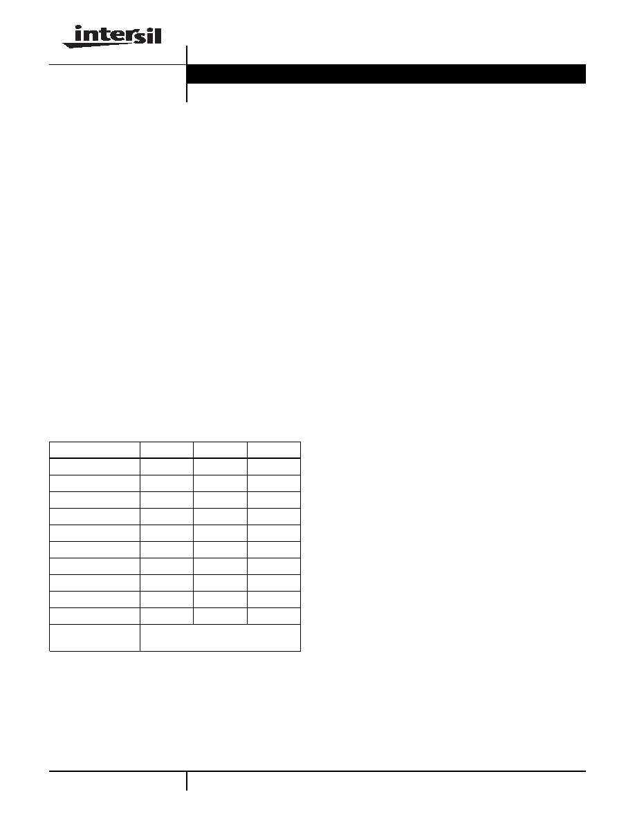
Table 1 summarizes the performance of this family.
TABLE 1. FEATURES AT A GLANCE
Features
∑ Fully Specified at
±
5V, 12V, 5V, and 3V Supplies for 10%
Tolerances
∑ Four Separately Controlled SPST Switches
∑ Pin Compatible with DG411/DG412/DG413
∑ ON Resistance (R
ON
) . . . . . . . . . . . . . . . . . . . . . . . . 50
∑ R
ON
Matching Between Channels. . . . . . . . . . . . . . . . . . . 2
∑ Low Charge Injection . . . . . . . . . . . . . . . . . . . . . . 5pC (Max)
∑ Low Power Consumption (P
D
). . . . . . . . . . . . . . . . . . . .<1
µ
W
∑ Low Leakage Current (Max at 85
o
C) . . . . . . . . . . . . . 5nA
∑ Fast Switching Action
- t
ON
. . . . . . . . . . . . . . . . . . . . . . . . . . . . . . . . . . . . 30ns
- t
OFF
. . . . . . . . . . . . . . . . . . . . . . . . . . . . . . . . . . . 18ns
∑ Guaranteed Break-Before-Make (ISL43142 only)
∑ Minimum 2000V ESD Protection per Method 3015.7
∑ TTL, CMOS Compatible
Applications
∑ Battery Powered, Handheld, and Portable Equipment
- Cellular/Mobile Phones
- Pagers
- Laptops, Notebooks, Palmtops
∑ Communications Systems
- Military Radios
- RF "Tee" Switches
∑ Test Equipment
- Ultrasound
- Electrocardiograph
∑ Heads-Up Displays
∑ Audio and Video Switching
∑ General Purpose Circuits
- +3V/+5V DACs and ADCs
- Digital Filters
- Operational Amplifier Gain Switching Networks
- High Frequency Analog Switching
- High Speed Multiplexing
Related Literature
∑ Technical Brief TB363 "Guidelines for Handling and
Processing Moisture Sensitive Surface Mount Devices
(SMDs)"
ISL43140
ISL43141
ISL43142
Number of Switches
4
4
4
Configuration
All NC
All NO
2 NC / 2 NO
10.8V R
ON
50
50
50
10.8V t
ON
/ t
OFF
30ns / 18ns
30ns / 18ns
30ns / 18ns
±
4.5V R
ON
50
50
50
±
4.5V t
ON
/ t
OFF
40ns / 15ns
40ns / 15ns
40ns / 15ns
4.5V R
ON
110
110
110
4.5V t
ON
/ t
OFF
50ns / 20ns
50ns / 20ns
50ns / 20ns
2.7V R
ON
200
200
200
2.7V t
ON
/ t
OFF
120ns / 25ns 120ns / 25ns 120ns / 25ns
Packages
16 Ld SOIC (N), 16 Ld 3x3 QFN,
16 Ld TSSOP
Data Sheet
November 2002
CAUTION: These devices are sensitive to electrostatic discharge; follow proper IC Handling Procedures.
1-888-INTERSIL or 321-724-7143
|
Intersil (and design) is a registered trademark of Intersil Americas Inc.
Copyright © Intersil Americas Inc. 2002. All Rights Reserved

2
Pinouts
(Note 1)
ISL43140 (SOIC, TSSOP)
TOP VIEW
ISL43140 (QFN)
TOP VIEW
ISL43141 (SOIC, TSSOP)
TOP VIEW
ISL43141 (QFN)
TOP VIEW
ISL43142 (SOIC, TSSOP)
TOP VIEW
ISL43142 (QFN)
TOP VIEW
NOTE:
1. Switches Shown for Logic "0" Input.
14
15
16
9
13
12
11
10
1
2
3
4
5
7
6
8
IN1
COM1
NC1
V-
GND
NC4
IN4
COM4
IN2
NC2
V+
N.C.
NC3
COM3
IN3
COM2
1
3
4
15
NC1
V-
GND
NC4
CO
M
1
IN
1
IN
2
CO
M
2
16
14
13
2
12
10
9
11
6
5
7
8
NC2
V+
N.C.
NC3
COM
4
IN
4
IN
3
COM
3
14
15
16
9
13
12
11
10
1
2
3
4
5
7
6
8
IN1
COM1
NO1
V-
GND
NO4
IN4
COM4
IN2
NO2
V+
N.C.
NO3
COM3
IN3
COM2
1
3
4
15
NO1
V-
GND
NO4
COM
1
IN1
IN2
COM
2
16
14
13
2
12
10
9
11
6
5
7
8
NO2
V+
N.C.
NO3
COM
4
IN4
IN3
COM
3
14
15
16
9
13
12
11
10
1
2
3
4
5
7
6
8
IN1
COM1
NO1
V-
GND
NO4
IN4
COM4
IN2
NC2
V+
N.C.
NC3
COM3
IN3
COM2
1
3
4
15
NO1
V-
GND
NO4
CO
M
1
IN
1
IN
2
CO
M
2
16
14
13
2
12
10
9
11
6
5
7
8
NC2
V+
N.C.
NC3
CO
M
4
IN4
IN3
CO
M
3
ISL43140, ISL43141, ISL43142

3
Truth Table
LOGIC
ISL43140
ISL43141
ISL43142
SW 1, 2, 3, 4 SW 1, 2, 3, 4 SW 1, 4 SW 2, 3
0
ON
OFF
OFF
ON
1
OFF
ON
ON
OFF
NOTE: Logic "0"
0.8V. Logic "1"
2.4V.
Pin Descriptions
PIN
FUNCTION
V+
Positive Power Supply Input
V-
Negative Power Supply Input. Connect to GND for
Single Supply Configurations.
GND
Ground Connection
IN
Digital Control Input
COM
Analog Switch Common Pin
NO
Analog Switch Normally Open Pin
NC
Analog Switch Normally Closed Pin
N.C.
No Internal Connection
Ordering Information
PART NO.
(BRAND)
(NOTE 2)
TEMP.
RANGE (
o
C)
PACKAGE
PKG. NO.
ISL43140IB
-40 to 85
16 Ld SOIC (N)
M16.15
ISL43140IR*
(140I)
-40 to 85
16 Ld QFN
L16.3x3
ISL43140IV
-40 to 85
16 Ld TSSOP
M16.173
ISL43141IB
-40 to 85
16 Ld SOIC (N)
M16.15
ISL43141IR*
(141I)
-40 to 85
16 Ld QFN
L16.3x3
ISL43141IV
-40 to 85
16 Ld TSSOP
M16.173
ISL43142IB
-40 to 85
16 Ld SOIC (N)
M16.15
ISL43142IR*
(142I)
-40 to 85
16 Ld QFN
L16.3x3
ISL43142IV
-40 to 85
16 Ld TSSOP
M16.173
NOTES:
2. Most surface mount devices are available on tape and reel; add
"-T" to suffix.
*
In Development.
ISL43140, ISL43141, ISL43142

4
Absolute Maximum Ratings
Thermal Information
V+ to V- . . . . . . . . . . . . . . . . . . . . . . . . . . . . . . . . . . . . . . -0.3 to15V
V+ to GND . . . . . . . . . . . . . . . . . . . . . . . . . . . . . . . . . . . . -0.3 to15V
V- to GND . . . . . . . . . . . . . . . . . . . . . . . . . . . . . . . . . . . -15 to 0.3V
All Other Pins (Note 3) . . . . . . . . . . . . . ((V-) - 0.3V) to ((V+) + 0.3V)
Continuous Current (Any Terminal) . . . . . . . . . . . . . . . . . . . . . 10mA
Peak Current, IN, NO, NC, or COM
(Pulsed 1ms, 10% Duty Cycle, Max) . . . . . . . . . . . . . . . . . . 20mA
ESD Rating (Per MIL-STD-883 Method 3015). . . . . . . . . . . . . .>2kV
Operating Conditions
Temperature Range
ISL4314XIX . . . . . . . . . . . . . . . . . . . . . . . . . . . . . . . . -40
o
C to 85
o
C
Thermal Resistance (Typical, Note 4)
JA
(
o
C/W)
16 Ld SOIC Package . . . . . . . . . . . . . . . . . . . . . . . .
115
16 Ld QFN Package. . . . . . . . . . . . . . . . . . . . . . . . .
75
16 Ld TSSOP Package . . . . . . . . . . . . . . . . . . . . . .
150
Maximum Junction Temperature (Plastic Package) . . . . . . . 150
o
C
Moisture Sensitivity (See Technical Brief TB363)
All Other Packages . . . . . . . . . . . . . . . . . . . . . . . . . . . . . . Level 1
QFN Package. . . . . . . . . . . . . . . . . . . . . . . . . . . . . . . . . . . Level 2
Maximum Storage Temperature Range. . . . . . . . . . . . -65
o
C to 150
o
C
Maximum Lead Temperature (Soldering 10s) . . . . . . . . . . . . 300
o
C
(SOIC and TSSOP - Lead Tips Only)
CAUTION: Stresses above those listed in "Absolute Maximum Ratings" may cause permanent damage to the device. This is a stress only rating and operation of the
device at these or any other conditions above those indicated in the operational sections of this specification is not implied.
NOTES:
3. Signals on NC, NO, COM, or IN exceeding V+ or V- are clamped by internal diodes. Limit forward diode current to maximum current ratings.
4.
JA
is measured with the component mounted on a low effective thermal conductivity test board in free air. See Tech Brief TB379 for details.
Electrical Specifications: ±5V Supply
Test Conditions V
SUPPLY
=
±
4.5V to
±
5.5V, GND = 0V, V
INH
= 2.4V, V
INL
= 0.8V (Note 5),
Unless Otherwise Specified
PARAMETER
TEST CONDITIONS
TEMP
(
o
C)
(NOTE 6)
MIN
TYP
(NOTE 6)
MAX
UNITS
ANALOG SWITCH CHARACTERISTICS
Analog Signal Range, V
ANALOG
Full
V-
-
V+
V
ON Resistance, R
ON
V
S
=
±
4.5V, I
COM
= 1.0mA, V
NO
or V
NC
=
±
3V,
See Figure 5
25
-
50
65
Full
-
-
75
R
ON
Matching Between Channels,
R
ON
V
S
=
±
4.5V, I
COM
= 1.0mA, V
NO
or V
NC
=
±
3V
25
-
2
2.5
Full
-
-
5
R
ON
Flatness, R
FLAT(ON)
V
S
=
±
4.5V, I
COM
= 1.0mA, V
NO
or V
NC
=
±
3V, Note 8
25
-
10
12
Full
-
-
13
NO or NC OFF Leakage Current,
I
NO(OFF)
or I
NC(OFF)
V
S
=
±
5.5V, V
COM
=
±
4.5V, V
NO
or V
NC
= +4.5V, Note
7
25
-1
0.01
1
nA
Full
-5
-
5
nA
COM OFF Leakage Current,
I
COM(OFF)
V
S
=
±
5.5V, V
COM
=
±
4.5V, V
NO
or V
NC
= +4.5V, Note
7
25
-1
0.01
1
nA
Full
-5
-
5
nA
COM ON Leakage Current,
I
COM(ON)
V
S
=
±
5.5V, V
COM
= V
NO
or V
NC
=
±
4.5V, Note 7
25
-2
0.01
2
nA
Full
-10
-
10
nA
DIGITAL INPUT CHARACTERISTICS
Input Voltage High, V
INH
Full
2.4
1.6
-
V
Input Voltage Low, V
INL
Full
-
1.6
0.8
V
Input Current, I
INH
, I
INL
V
S
=
±
5.5V, V
IN
= 0V or V+
Full
-0.5
0.03
0.5
µ
A
DYNAMIC CHARACTERISTICS
Turn-ON Time, t
ON
V
S
=
±
4.5V, V
NO
or V
NC
=
±
3V, R
L
= 300
, C
L
= 35pF,
V
IN
= 0 to 3V, See Figure 1
25
-
40
80
ns
Full
-
-
100
ns
Turn-OFF Time, t
OFF
V
S
=
±
4.5V, V
NO
or V
NC
=
±
3V, R
L
= 300
, C
L
= 35pF,
V
IN
= 0 to 3V, See Figure 1
25
-
15
30
ns
Full
-
-
40
ns
Break-Before-Make Time Delay
(ISL43142), t
D
V
S
=
±
5.5V, V
NO
or V
NC
=
±
3V, R
L
= 300
, C
L
= 35pF,
V
IN
= 0 to 3V, See Figure 3
Full
5
20
-
ns
Charge Injection, Q
C
L
= 1.0nF, V
G
= 0V, R
G
= 0
, See Figure 2
25
-
1
5
pC
NO or NC OFF Capacitance, C
OFF
f = 1MHz, V
NO
or V
NC
= V
COM
= 0V, See Figure 7
25
-
7
-
pF
COM OFF Capacitance,
C
COM(OFF)
f = 1MHz, V
NO
or V
NC
= V
COM
= 0V, See Figure 7
25
-
7
-
pF
COM ON Capacitance, C
COM(ON)
f = 1MHz, V
NO
or V
NC
= V
COM
= 0V, See Figure 7
25
-
14
-
pF
ISL43140, ISL43141, ISL43142

5
OFF Isolation
R
L
= 50
, C
L
= 15pF, f = 100kHz,
V
NO
or V
NC
= 1V
RMS
, See Figures 4, 6, and 19
25
-
>90
-
dB
Crosstalk, Note 9
25
-
<-90
-
dB
All Hostile Crosstalk
R
L
= 50
, C
L
= 15pF, f = 10MHz,
V
NO
or V
NC
= 1V
RMS
, See Figure 19
25
-
-60
-
dB
Power Supply Rejection Ratio
R
L
= 50
, C
L
= 15pF, f = 1MHz, See Figure 20
25
-
60
-
dB
POWER SUPPLY CHARACTERISTICS
Power Supply Range
Full
±
2
-
±
6
V
Positive Supply Current, I+
V
S
=
±
5.5V, V
IN
= 0V or V+, Switch On or Off
25
-1
0.05
1
µ
A
Full
-1
-
1
µ
A
Negative Supply Current, I-
25
-1
0.05
1
µ
A
Full
-1
-
1
µ
A
NOTES:
5. V
IN
= Input voltage to perform proper function.
6. The algebraic convention, whereby the most negative value is a minimum and the most positive a maximum, is used in this data sheet.
7. Leakage parameter is 100% tested at high temp, and guaranteed by correlation at 25
o
C.
8. Flatness is defined as the delta between the maximum and minimum R
ON
values over the specified voltage range.
9. Between any two switches.
Electrical Specifications: 12V Supply
Test Conditions: V+ = +10.8V to +13.2V, V- = GND = 0V, V
INH
= 5V, V
INL
= 0.8V (Note 5),
Unless Otherwise Specified
PARAMETER
TEST CONDITIONS
TEMP
(
o
C)
(NOTE 6)
MIN
TYP
(NOTE 6)
MAX
UNITS
ANALOG SWITCH CHARACTERISTICS
Analog Signal Range, V
ANALOG
Full
0
-
V+
V
ON Resistance, R
ON
V+ = 10.8V, I
COM
= 1.0mA, V
NO
or V
NC
= 9V,
See Figure 5
25
-
50
65
Full
-
60
75
R
ON
Matching Between Channels,
R
ON
V+ = 10.8V, I
COM
= 1.0mA, V
NO
or V
NC
= 9V
25
-
2
2.5
Full
-
-
5
R
ON
Flatness, R
FLAT(ON)
V+ = 10.8V, I
COM
= 1.0mA, V
NO
or V
NC
= 3V, 6V, 9V,
Note 8
25
-
8
12
Full
-
9
13
NO or NC OFF Leakage Current,
I
NO(OFF)
or I
NC(OFF)
V+ = 13.2V, V
COM
= 1V, 10V, V
NO
or V
NC
= 10V, 1V,
Note 7
25
-1
-
1
nA
Full
-5
-
5
nA
COM OFF Leakage Current,
I
COM(OFF)
V+ = 13.2V, V
COM
= 10V, 1V, V
NO
or V
NC
= 1V, 10V,
Note 7
25
-1
-
1
nA
Full
-5
-
5
nA
COM ON Leakage Current,
I
COM(ON)
V
+
= 13.2V, V
COM
= 1V, 10V, or V
NO
or V
NC
= 1V,
10V, Note 7
25
-2
-
2
nA
Full
-10
-
10
nA
DIGITAL INPUT CHARACTERISTICS
Input Voltage High, V
INH
Full
3.5
3.1
-
V
Input Voltage Low, V
INL
Full
-
-
0.8
V
Input Current, I
INH
, I
INL
V+ = 13.2V, V
IN
= 0V or V+
Full
-1
-
1
µ
A
DYNAMIC CHARACTERISTICS
Turn-ON Time, t
ON
V+ = 10.8V, V
NO
or V
NC
= 10V, R
L
= 300
, C
L
= 35pF,
V
IN
= 0 to 3.3V, See Figure 1
25
-
30
70
ns
Full
-
34
100
ns
Turn-OFF Time, t
OFF
V+ = 10.8V, V
NO
or V
NC
= 10V, R
L
= 300
, C
L
= 35pF,
V
IN
= 0 to 3.3V, See Figure 1
25
-
18
50
ns
Full
-
20
75
ns
Break-Before-Make Time Delay
(ISL43142), t
D
V+ = 13.2V, V
NO
or V
NC
= 10V, R
L
= 300
, C
L
= 35pF,
V
IN
= 0 to 3.3V, See Figure 3
Full
0
8
-
ns
Electrical Specifications: ±5V Supply
Test Conditions V
SUPPLY
=
±
4.5V to
±
5.5V, GND = 0V, V
INH
= 2.4V, V
INL
= 0.8V (Note 5),
Unless Otherwise Specified (Continued)
PARAMETER
TEST CONDITIONS
TEMP
(
o
C)
(NOTE 6)
MIN
TYP
(NOTE 6)
MAX
UNITS
ISL43140, ISL43141, ISL43142