Äîêóìåíòàöèÿ è îïèñàíèÿ www.docs.chipfind.ru
1
®
FN6049.3
ISL4485E
±
15kV ESD Protected, 20Mbps, 5V, Low
Power, RS-485/RS-422 Transceiver
The Intersil ISL4485E is a high speed, BiCMOS 5V
powered, single transceiver that meets both the RS-485 and
RS-422 standards for balanced communication. Each driver
output/receiver input is protected against ±15kV ESD
strikes, without latch-up. Unlike competitive devices, this
Intersil device is specified for 10% tolerance supplies (4.5V
to 5.5V).
The excellent differential output voltage coupled with high
drive-current output stages allow 20Mbps operation over
twisted pair networks up to 450 feet in length. The 25k
receiver input resistance presents a "single unit load" to the
RS-485 bus, allowing up to 32 transceivers on the network.
Receiver (Rx) inputs feature a "fail-safe if open" design,
which ensures a logic high Rx output if Rx inputs are
floating.
Driver (Tx) outputs are short circuit protected, even for
voltages exceeding the power supply voltage. Additionally,
on-chip thermal shutdown circuitry disables the Tx outputs to
prevent damage if power dissipation becomes excessive.
The half duplex configuration multiplexes the Rx inputs and
Tx outputs to allow transceivers with Rx and Tx disable
functions in 8 lead packages.
Features
·
Pb-Free Available (RoHS Compliant)
· High Data Rates. . . . . . . . . . . . . . . . . . . . . up to 20Mbps
· RS-485 I/O Pin ESD Protection . . . . . . . . . .
±
15kV HBM
- Class 3 ESD Level on all Other Pins . . . . . . >7kV HBM
· Operates from a Single +5V Supply (10% Tolerance)
· 1 Unit Load Allows up to 32 Devices on the Bus
· Low Quiescent Current . . . . . . . . . . . . . . . . . . . . . 700
µ
A
· -7V to +12V Common Mode Input Voltage Range
· Three State Rx and Tx Outputs
· 30ns Propagation Delays, 2ns Skew
· Current Limiting and Thermal Shutdown for driver
Overload Protection
Applications
· SCSI "Fast 20" Drivers and Receivers
· Data Loggers
· Security Networks
· Building Environmental Control Systems
· Industrial/Process Control Networks
· Level Translators
Pinout
ISL4485E (SOIC)
TOP VIEW
Ordering Information
PART NO.
(BRAND)
TEMP.
RANGE (
o
C)
PACKAGE
PKG. DWG. #
ISL4485EIB
(4485EIB)
-40 to 85
8 Ld SOIC
M8.15
ISL4485EIBZ
(4485EIBZ)
(See Note)
-40 to 85
8 Ld SOIC
(Pb-free)
M8.15
ISL4485EIB-T
(4485EIB)
-40 to 85
8 Ld SOIC
Tape & Reel
M8.15
ISL4485EIBZ-T
(4485EIBZ)
(See Note)
-40 to 85
8 Ld SOIC
Tape & Reel
(Pb-free)
M8.15
NOTE: Intersil Pb-free products employ special Pb-free material sets;
molding compounds/die attach materials and 100% matte tin plate
termination finish, which are RoHS compliant and compatible with
both SnPb and Pb-free soldering operations. Intersil Pb-free products
are MSL classified at Pb-free peak reflow temperatures that meet or
exceed the Pb-free requirements of IPC/JEDEC J STD-020.
RO
RE
DE
DI
1
2
3
4
8
7
6
5
V
CC
B / Z
A / Y
GND
D
R
Data Sheet
April 21, 2005
CAUTION: These devices are sensitive to electrostatic discharge; follow proper IC Handling Procedures.
1-888-INTERSIL or 321-724-7143
|
Intersil (and design) is a registered trademark of Intersil Americas Inc.
Copyright © Intersil Americas Inc. 2004, 2005. All Rights Reserved.
All other trademarks mentioned are the property of their respective owners.
2
Truth Tables
TRANSMITTING
INPUTS
OUTPUTS
RE
DE
DI
B/Z
A/Y
X
1
1
0
1
X
1
0
1
0
X
0
X
High-Z
High-Z
RECEIVING
INPUTS
OUTPUT
RE
DE
A-B
RO
0
0
+0.2V
1
0
0
-0.2V
0
0
0
Inputs Open
1
1
X
X
High-Z
Pin Descriptions
PIN
FUNCTION
RO
Receiver output: If A > B by at least 0.2V, RO is high; If A < B by 0.2V or more, RO is low; RO = High if A and B are unconnected (floating).
RE
Receiver output enable. RO is enabled when RE is low; RO is high impedance when RE is high.
DE
Driver output enable. The driver outputs, Y and Z, are enabled by bringing DE high. They are high impedance when DE is low.
DI
Driver input. A low on DI forces output Y low and output Z high. Similarly, a high on DI forces output Y high and output Z low.
GND
Ground connection.
A/Y
±
15kV HBM ESD Protected, noninverting receiver input and noninverting driver output. Pin is an input (A) if DE = 0; pin is an output
(Y) if DE = 1.
B/Z
±
15kV HBM ESD Protected, inverting receiver input and inverting driver output. Pin is an input (B) if DE = 0; pin is an output (Z) if
DE = 1.
V
CC
System power supply input (4.5V to 5.5V).
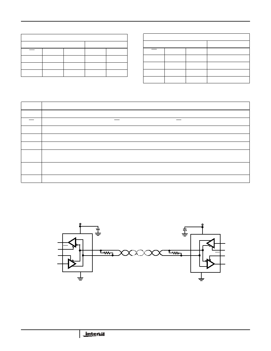
Typical Operating Circuit
0.1
µ
F
+
D
R
7
6
8
1
2
3
4
5
V
CC
GND
RO
RE
DE
DI
A/Y
B/Z
+5V
0.1
µ
F
+
D
R
6
7
8
1
2
3
4
5
V
CC
GND
RO
RE
DE
DI
A/Y
B/Z
+5V
R
T
R
T
ISL4485E
ISL4485E
3
Absolute Maximum Ratings
Thermal Information
V
CC
to Ground. . . . . . . . . . . . . . . . . . . . . . . . . . . . . . . . . . . . . . . 7V
Input Voltages
DI, DE, RE . . . . . . . . . . . . . . . . . . . . . . . . . . -0.5V to (V
CC
+0.5V)
Input / Output Voltages
A / Y, B / Z . . . . . . . . . . . . . . . . . . . . . . . . . . . . . . . -8V to +12.5V
RO . . . . . . . . . . . . . . . . . . . . . . . . . . . . . . . . -0.5V to (V
CC
+0.5V)
Short Circuit Duration
Y, Z. . . . . . . . . . . . . . . . . . . . . . . . . . . . . . . . . . . . . . . Continuous
ESD Rating . . . . . . . . . . . . . . . . . . . . . . . . . See Specification Table
Operating Conditions
Temperature Range
ISL4485EIB . . . . . . . . . . . . . . . . . . . . . . . . . . . . . . -40
o
C to 85
o
C
Thermal Resistance (Typical, Note 1)
JA
(
o
C/W)
8 Ld SOIC Package . . . . . . . . . . . . . . . . . . . . . . . . .
170
Maximum Junction Temperature (Plastic Package) . . . . . . . 150
o
C
Maximum Storage Temperature Range . . . . . . . . . -65
o
C to 150
o
C
Maximum Lead Temperature (Soldering 10s) . . . . . . . . . . . . 300
o
C
(Lead Tips Only)
CAUTION: Stresses above those listed in "Absolute Maximum Ratings" may cause permanent damage to the device. This is a stress only rating and operation of the
device at these or any other conditions above those indicated in the operational sections of this specification is not implied.
NOTE:
1.
JA
is measured with the component mounted on a low effective thermal conductivity test board in free air. See Tech Brief TB379 for details.
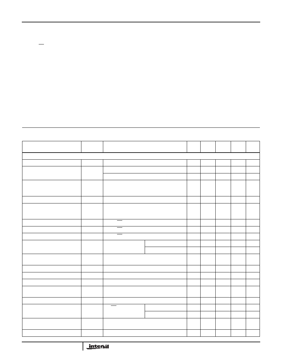
Electrical Specifications
Test Conditions: V
CC
= 4.5V to 5.5V; Unless Otherwise Specified.
Typicals are at V
CC
= 5V, T
A
= 25
o
C, Note 2
PARAMETER
SYMBOL
TEST CONDITIONS
TEMP
(
o
C)
MIN
TYP
MAX
UNITS
DC CHARACTERISTICS
Driver Differential V
OUT
(no load)
V
OD1
Full
-
-
V
CC
V
Driver Differential V
OUT
(with load)
V
OD2
R = 50
(RS-422), (Figure 1)
Full
2
3
-
V
R = 27
(RS-485), (Figure 1)
Full
1.5
2.3
5
V
Change in Magnitude of Driver
Differential V
OUT
for
Complementary Output States
V
OD
R = 27
or 50
, (Figure 1)
Full
-
0.01
0.2
V
Driver Common-Mode V
OUT
V
OC
R = 27
or 50
, (Figure 1)
Full
-
-
3
V
Change in Magnitude of Driver
Common-Mode V
OUT
for
Complementary Output States
V
OC
R = 27
or 50
, (Figure 1)
Full
-
0.01
0.2
V
Logic Input High Voltage
V
IH
DE, DI, RE
Full
2
-
-
V
Logic Input Low Voltage
V
IL
DE, DI, RE
Full
-
-
0.8
V
Logic Input Current
I
IN1
DE, DI, RE
Full
-25
-
25
µ
A
Input Current (A, B), (Note 5)
I
IN2
DE = 0V, V
CC
= 0V or
4.5 to 5.5V
V
IN
= 12V
Full
-
-
1
mA
V
IN
= -7V
Full
-
-
-0.8
mA
Receiver Differential Threshold
Voltage
V
TH
-7V
V
CM
12V
Full
-0.2
-
0.2
V
Receiver Input Hysteresis
V
TH
V
CM
= 0V
25
-
70
-
mV
Receiver Output High Voltage
V
OH
I
O
= -4mA, V
ID
= 200mV
Full
3.5
4
-
V
Receiver Output Low Voltage
V
OL
I
O
= -4mA, V
ID
= 200mV
Full
-
0.1
0.4
V
Three-State (high impedance)
Receiver Output Current
I
OZR
0.4V
V
O
2.4V
Full
-
-
±
1
µ
A
Receiver Input Resistance
R
IN
-7V
V
CM
12V
Full
12
25
-
k
No-Load Supply Current, (Note 3)
I
CC
DI, RE = 0V or V
CC
DE = V
CC
Full
-
700
900
µ
A
DE = 0V
Full
-
500
565
µ
A
Driver Short-Circuit Current,
V
O
= High or Low
I
OSD1
DE = V
CC
, -7V
V
Y
or V
Z
12V, (Note 4)
Full
35
-
250
mA
Receiver Short-Circuit Current
I
OSR
0V
V
O
V
CC
Full
7
-
85
mA
ISL4485E
4
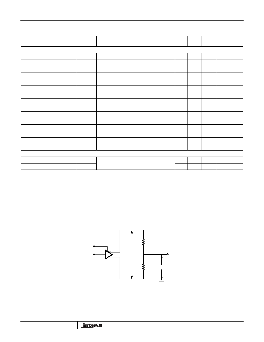
SWITCHING CHARACTERISTICS
Driver Input to Output Delay
t
PLH
, t
PHL
R
DIFF
= 54
, C
L
= 100pF, (Figure 2)
Full
15
30
50
ns
Driver Output Skew
t
SKEW
R
DIFF
= 54
, C
L
= 100pF, (Figure 2)
Full
-
1.3
5
ns
Driver Differential Rise or Fall Time
t
R
, t
F
R
DIFF
= 54
, C
L
= 100pF, (Figure 2)
Full
3
11
25
ns
Driver Enable to Output High
t
ZH
C
L
= 100pF, SW = GND, (Figure 3)
Full
-
17
30
ns
Driver Enable to Output Low
t
ZL
C
L
= 100pF, SW = V
CC
, (Figure 3)
Full
-
14
30
ns
Driver Disable from Output High
t
HZ
C
L
= 15pF, SW = GND, (Figure 3)
Full
-
19
30
ns
Driver Disable from Output Low
t
LZ
C
L
= 15pF, SW = V
CC
, (Figure 3)
Full
-
13
30
ns
Driver Maximum Data Rate
f
MAXD
V
OD
1.5V
, (Figure 4, Note 6)
Full
20
-
-
Mbps
Receiver Input to Output Delay
t
PLH
, t
PHL
Figure 5
Full
20
40
70
ns
Receiver Skew | t
PLH
- t
PHL
|
t
SKD
Figure 5
Full
-
3
10
ns
Receiver Enable to Output High
t
ZH
C
L
= 15pF, SW = GND, (Figure 6)
Full
-
9
25
ns
Receiver Enable to Output Low
t
ZL
C
L
= 15pF, SW = V
CC
, (Figure 6)
Full
-
9
25
ns
Receiver Disable from Output High
t
HZ
C
L
= 15pF, SW = GND, (Figure 6)
Full
-
9
25
ns
Receiver Disable from Output Low
t
LZ
C
L
= 15pF, SW = V
CC
, (Figure 6)
Full
-
9
25
ns
Receiver Maximum Data Rate
f
MAXR
C
L
= 15pF, V
ID
1.5V (Note 6)
Full
20
-
-
Mbps
ESD PERFORMANCE
RS-485 Pins (A/Y, B/Z)
Human Body Model
25
-
±
15
-
kV
All Other Pins
25
-
>
±
7
-
kV
NOTE:
2. All currents into device pins are positive; all currents out of device pins are negative. All voltages are referenced to device ground unless
otherwise specified.
3. Supply current specification is valid for loaded drivers when DE = 0V.
4. Applies to peak current. See "Typical Performance Curves" for more information.
5. Devices meeting these limits are denoted as "single unit load (1 UL)" transceivers. The RS-485 standard allows up to 32 Unit Loads on the bus.
6. Guaranteed by characterization, but not tested.
Test Circuits and Waveforms
FIGURE 1. DRIVER V
OD
AND V
OC
Electrical Specifications
Test Conditions: V
CC
= 4.5V to 5.5V; Unless Otherwise Specified.
Typicals are at V
CC
= 5V, T
A
= 25
o
C, Note 2 (Continued)
PARAMETER
SYMBOL
TEST CONDITIONS
TEMP
(
o
C)
MIN
TYP
MAX
UNITS
D
DE
DI
V
CC
V
OD
V
OC
R
R
Z
Y
ISL4485E
5
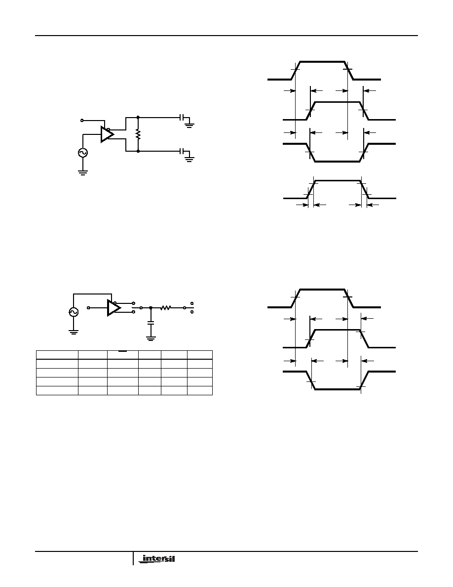
FIGURE 2A. TEST CIRCUIT
FIGURE 2B. MEASUREMENT POINTS
FIGURE 2. DRIVER PROPAGATION DELAY AND DIFFERENTIAL TRANSITION TIMES
FIGURE 3A. TEST CIRCUIT
FIGURE 3B. MEASUREMENT POINTS
FIGURE 3. DRIVER ENABLE AND DISABLE TIMES
Test Circuits and Waveforms
(Continued)
D
DE
DI
V
CC
SIGNAL
GENERATOR
C
L
= 100pF
R
DIFF
Z
Y
C
L
= 100pF
OUT (Y)
3V
0V
t
PLH
1.5V
1.5V
V
OH
V
OL
50%
50%
t
PHL
OUT (Z)
t
PHL
V
OH
V
OL
50%
50%
t
PLH
DIFF OUT (Y - Z)
t
R
+V
OD
-V
OD
90%
90%
t
F
10%
10%
DI
SKEW = |CROSSING PT. OF Y
& Z
- CROSSING PT. OF Y
& Z
|
D
DE
DI
C
L
500
Z
Y
V
CC
GND
SW
PARAMETER OUTPUT
RE
DI
SW
C
L
(pF)
t
HZ
Y/Z
X
1/0
GND
15
t
LZ
Y/Z
X
0/1
V
CC
15
t
ZH
Y/Z
X
1/0
GND
100
t
ZL
Y/Z
X
0/1
V
CC
100
SIGNAL
GENERATOR
OUT (Y, Z)
3V
0V
1.5V
1.5V
V
OH
0V
2.3V
V
OH
- 0.5V
t
HZ
OUT (Y, Z)
V
CC
V
OL
2.3V
V
OL
+ 0.5V
t
LZ
DE
OUTPUT HIGH
OUTPUT LOW
t
ZL
t
ZH
ISL4485E