
1
Æ
FN6162.1
CAUTION: These devices are sensitive to electrostatic discharge; follow proper IC Handling Procedures.
1-888-INTERSIL or 1-888-468-3774
|
Intersil (and design) is a registered trademark of Intersil Americas Inc.
Copyright © Intersil Americas Inc. 2005. All Rights Reserved.
All other trademarks mentioned are the property of their respective owners.
ISL59440
400MHz Multiplexing Amplifier
The ISL59440 is a 400MHz bandwidth 4:1 multiplexing
amplifier designed primarily for video switching. This Mux-
amp has user-settable gain and also features a high speed
three-state function to enable the output of multiple devices to
be wired together. All logic inputs have pull-downs to ground
and may be left floating. The ENABLE pin, when pulled high,
sets the ISL59440 to the low current power-down mode for
power sensitive applications - consuming just 5mW.
Features
∑ 411MHz (-3dB) Bandwidth (A
V
= 1, V
OUT
= 100mV
P-P
)
∑ 200MHz (-3dB) Bandwidth (A
V
= 2, V
OUT
= 2V
P-P
)
∑ Slew Rate (A
V
= 1, R
L
= 500
,
V
OUT
= 4V) . . . . .1053V
/
µs
∑ Slew Rate (A
V
= 2, R
L
= 500
,
V
OUT
= 5V) . . . . .1470V
/
µs
∑ Adjustable Gain
∑ High Speed Three-state Output (HIZ)
∑ Low Current Power-down. . . . . . . . . . . . . . . . . . . . . .5mW
∑ Pb-Free Plus Anneal Available (RoHS Compliant)
Applications
∑ HDTV/DTV Analog Inputs
∑ Video Projectors
∑ Computer Monitors
∑ Set-top Boxes
∑ Security Video
∑ Broadcast Video Equipment
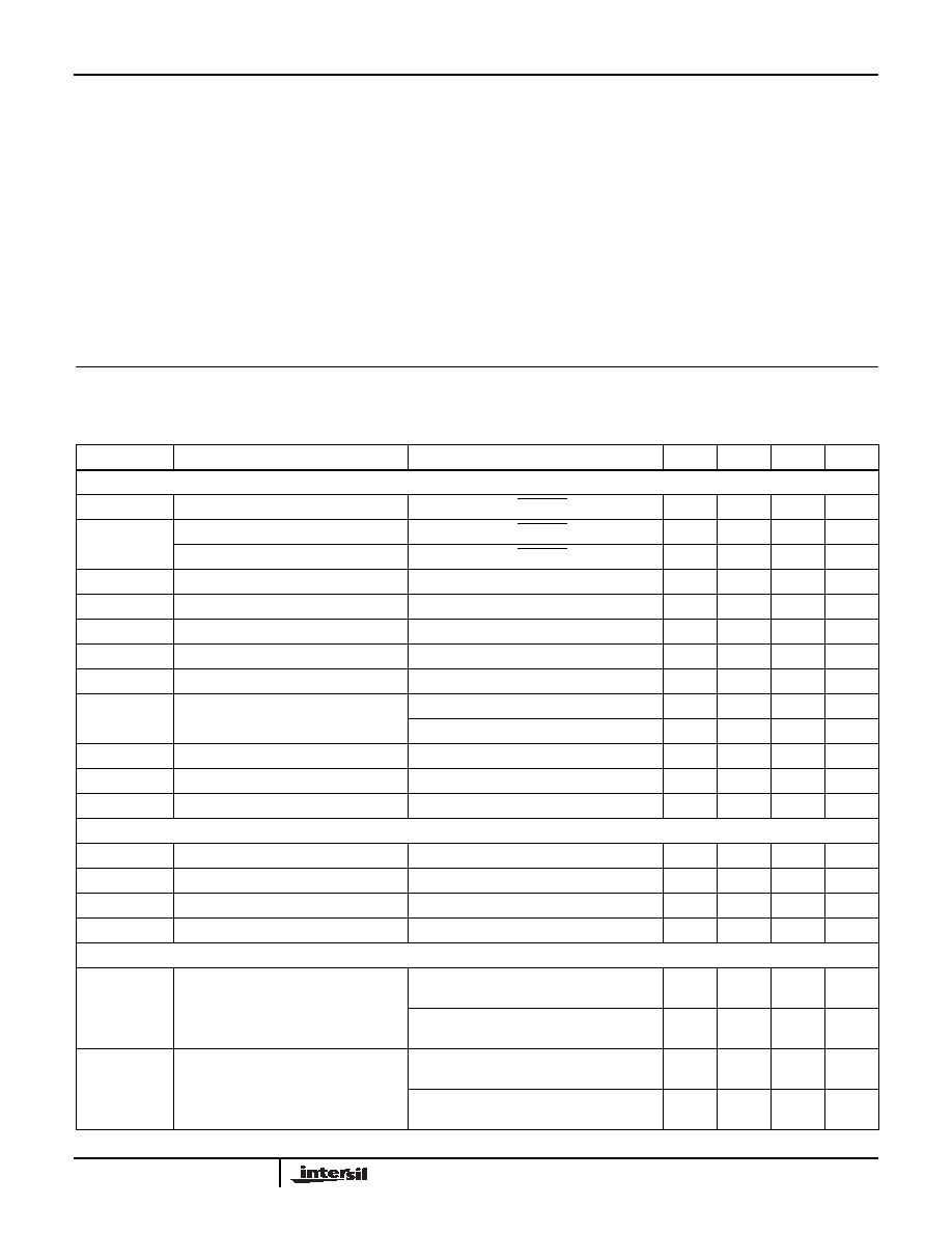
TABLE 1. CHANNEL SELECT LOGIC TABLE
S1
S0
ENABLE
HIZ
OUTPUT
0
0
0
0
IN0
0
1
0
0
IN1
1
0
0
0
IN2
1
1
0
0
IN3
X
X
1
X
Power Down
X
X
0
1
High Z
Pinout
ISL59440 (16 Ld QSOP)
TOP VIEW
Functional Diagram
1
2
3
4
16
15
14
13
5
6
7
12
11
10
8
9
NIC
IN0
NIC
IN3
ENABLE
HIZ
IN-
V+
S0
IN1
GND
IN2
NIC
OUT
V-
S1
-
+
DECODE
IN0
IN1
IN2
IN3
S0
S1
EN0
EN1
EN3
EN2
HIZ
ENABLE
AMPLIFIER BIAS
OUT
+
-
IN-
ENABLE pin must be low in order to activate the HIZ state
Ordering Information
PART NUMBER
PART
MARKING
PACKAGE
TAPE &
REEL
PKG.
DWG. #
ISL59440IA
ISL59440IA
16 Ld QSOP
-
MDP0040
ISL59440IA-T7
ISL59440IA
16 Ld QSOP
7"
MDP0040
ISL59440IA-T13
ISL59440IA
16 Ld QSOP
13"
MDP0040
ISL59440IAZ
(Note)
ISL59440IAZ 16 Ld QSOP
(Pb-free)
-
MDP0040
ISL59440IAZ-T7
(Note)
ISL59440IAZ 16 Ld QSOP
(Pb-free)
7"
MDP0040
ISL59440IAZ-T13
(Note)
ISL59440IAZ 16 Ld QSOP
(Pb-free)
13"
MDP0040
NOTE: Intersil Pb-free plus anneal products employ special Pb-free
material sets; molding compounds/die attach materials and 100% matte
tin plate termination finish, which are RoHS compliant and compatible
with both SnPb and Pb-free soldering operations. Intersil Pb-free
products are MSL classified at Pb-free peak reflow temperatures that
meet or exceed the Pb-free requirements of IPC/JEDEC J STD-020.
Data Sheet
September 21, 2005
2
FN6162.1
September 21, 2005
Absolute Maximum Ratings
(T
A
= 25∞C)
Supply Voltage (V+ to V-) . . . . . . . . . . . . . . . . . . . . . . . . . . . . . . 11V
Input Voltage . . . . . . . . . . . . . . . . . . . . . . . . . . . . V- -0.5V, V+ +0.5V
Supply Turn-on Slew Rate . . . . . . . . . . . . . . . . . . . . . . . . . . . 1V/
µs
IN- Input Current (Note 1) . . . . . . . . . . . . . . . . . . . . . . . . . . . . . 5mA
Digital & Analog Input Current (Note 1) . . . . . . . . . . . . . . . . . . 50mA
Output Current (Continuous) . . . . . . . . . . . . . . . . . . . . . . . . . . 50mA
ESD Rating
Human Body Model (Per MIL-STD-883 Method 3015.7). . . . 2.5kV
Machine Model . . . . . . . . . . . . . . . . . . . . . . . . . . . . . . . . . . . 300V
Storage Temperature Range . . . . . . . . . . . . . . . . . . -65∞C to +150∞C
Ambient Operating Temperature . . . . . . . . . . . . . . . . -40∞C to +85∞C
Operating Junction Temperature . . . . . . . . . . . . . . . -40∞C to +125∞C
Power Dissipation . . . . . . . . . . . . . . . . . . . . . . . . . . . . . .See Curves
JA
. . . . . . . . . . . . . . . . . . . . . . . . . . . . . . . . . . . . . . . . . .See Curves
CAUTION: Stresses above those listed in "Absolute Maximum Ratings" may cause permanent damage to the device. This is a stress only rating and operation of the
device at these or any other conditions above those indicated in the operational sections of this specification is not implied.
NOTE:
1. If an input signal is applied before the supplies are powered up, the input current must be limited to these maximum values.
IMPORTANT NOTE: All parameters having Min/Max specifications are guaranteed. Typical values are for information purposes only. Unless otherwise noted, all tests
are at the specified temperature and are pulsed tests, therefore: T
J
= T
C
= T
A
Electrical Specifications
V+ = +5V, V- = -5V, GND = 0V, T
A
= 25
∞
C, R
L
= 500
to GND unless otherwise specified.
PARAMETER
DESCRIPTION
CONDITIONS
MIN
TYP
MAX
UNIT
GENERAL
±
I
S
Enabled
Supply Current
No load, V
IN
= 0V, ENABLE
Low
12.5
14.5
16.5
mA
I
S
Disabled
Disabled Supply Current I+
No load, V
IN
= 0V, ENABLE
High
0.5
1
1.5
mA
Disabled Supply Current I-
No load, V
IN
= 0V, ENABLE
High
3
10
µA
V
OUT
Positive and Negative Output Swing
V
IN
=
±
2V, R
L
= 500
, A
V
= 2
±
3.5
±
3.9
V
I
OUT
Output Current
R
L
= 10
to GND
80
130
mA
V
OS
Output Offset Voltage
-12
4
+12
mV
Ib+
Input Bias Current
V
IN
= 0V
-4
2.5
-1.5
µA
Ib-
Feedback Bias Current
-15
7
15
µA
R
out
Output Resistance
HIZ = logic high, (DC), A
V
=1
1.4
M
HIZ = logic low, (DC), A
V
=1
0.2
R
IN
Input Resistance
V
IN
= 3.5V
10
M
A
CL
or A
V
Voltage Gain
R
F
= R
G
= 500
, V
OUT
=
±
3V
1.990
2.005
2.020
V/V
I
TRI
Output Current in Three-state
V
OUT
= 0V
-20
6
20
µA
LOGIC
V
H
Input High Voltage (Logic Inputs)
2
V
V
L
Input Low Voltage (Logic Inputs)
0.8
V
I
IH
Input High Current (Logic Inputs)
55
90
135
A
I
IL
Input Low Current (Logic Inputs)
-10
0
10
A
AC GENERAL
- 3dB BW
-3dB Bandwidth
A
V
= 1, R
F
= 332
, V
OUT
= 200mV
P-P
,
C
L
= 1.6pF, C
G
= 0.6pF
400
MHz
A
V
= 2, R
F
= R
G
= 511
, V
OUT
= 2V
P-P
,
C
L
= 5.5pF, C
G
= 0.6pF
200
MHz
0.1dB BW
0.1dB Bandwidth
A
V
= 1, R
F
= 332
, V
OUT
= 200mV
P-P
,
C
L
= 1.6pF, C
G
= 0.6pF
22
MHz
A
V
= 2, R
F
= R
G
= 511
, V
OUT
= 2V
P-P
,
C
L
= 5.5pF, C
G
= 0.6pF
62
MHz
ISL59440

3
FN6162.1
September 21, 2005
dG
Differential Gain Error
NTC-7, R
L
= 150, C
L
= 1.6pF, A
V
= 1
0.01
%
NTC-7, R
L
= 150, C
L
= 5.5pF, A
V
= 2
0.05
%
dP
Differential Phase Error
NTC-7, R
L
= 150, C
L
= 1.6pF, A
V
= 1
0.02
∞
NTC-7, R
L
= 150, C
L
= 5.5pF, A
V
= 2
0.02
∞
+SR
Slew Rate
25% to 75%, A
V
= 1, V
OUT
= 4V, R
L
= 500
,
C
L
= 1.6pF
1053
V/
µ
s
25% to 75%, A
V
= 2, V
OUT
= 5V, R
L
= 500
,
C
L
= 5.5pF
1470
V/
µ
s
-SR
Slew Rate
25% to 75%, A
V
= 1, V
OUT
= 4V, R
L
= 500
,
C
L
= 1.6pF
925
V/
µ
s
25% to 75%, A
V
= 2, V
OUT
= 5V, R
L
= 500
,
C
L
= 5.5pF
1309
V/
µ
s
PSRR
Power Supply Rejection Ratio
DC, PSRR V+ & V- combined
-50
-58
dB
ISO
Channel Isolation
f = 10MHz, Ch-Ch X-Talk and Off Isolation,
C
L
= 5.5pF
75
dB
SWITCHING CHARACTERISTICS
V
GLITCH
Channel-to-Channel Switching Glitch
V
IN
= 0V, C
L
= 5.5pF, A
V
= 2
1
mV
P-P
ENABLE Switching Glitch
V
IN
= 0V, C
L
= 5.5pF, A
V
= 2
800
mV
P-P
HIZ Switching Glitch
V
IN
= 0V, C
L
= 5.5pF, A
V
= 2
375
mV
P-P
t
SW-L-H
Channel Switching Time Low to High
1.2V logic threshold to 10% movement of
analog output
25
ns
t
SW-H-L
Channel Switching Time High to Low
1.2V logic threshold to 10% movement of
analog output
20
ns
TRANSIENT RESPONSE
t
R,
t
F
Rise & Fall Time, 10% to 90%
A
V
= 1, R
F
= 332
, V
OUT
= 100mV
P-P
,
C
L
= 1.6pF, C
G
= 0.6pF
0.65
ns
A
V
= 2, R
F
= R
G
= 511
, V
OUT
= 2V
P-P
,
C
L
= 5.5pF, C
G
= 0.6pF
1.51
ns
t
S
0.1% Settling Time
A
V
= 2, R
F
= R
G
= 511
, V
OUT
= 2V
P-P
,
C
L
= 5.5pF, C
G
= 0.6pF
9.0
ns
O
S
Overshoot
A
V
= 1, R
F
= 332
, V
OUT
= 100mV
P-P
,
C
L
= 1.6pF, C
G
= 0.6pF
17.85
%
A
V
= 2, R
F
= R
G
= 511
, V
OUT
= 2V
P-P
,
C
L
= 5.5pF, C
G
= 0.6pF
12.65
%
t
PLH
Propagation Delay - Low to High,
10% to 10%
A
V
= 1, R
F
= 332
, V
OUT
= 100mV
P-P
,
C
L
= 1.6pF, C
G
= 0.6pF
0.54
ns
A
V
= 2, R
F
= R
G
= 511
, V
OUT
= 2V
P-P
,
C
L
= 5.5pF, C
G
= 0.6pF
0.99
ns
t
PHL
Propagation Delay- High to Low,
10% to 10%
A
V
= 1, R
F
= 332
, V
OUT
= 100mV
P-P
,
C
L
= 1.6pF, C
G
= 0.6pF
0.57
ns
A
V
= 2, R
F
= R
G
= 511
, V
OUT
= 2V
P-P
,
C
L
= 5.5pF, C
G
= 0.6pF
1.02
ns
Electrical Specifications
V+ = +5V, V- = -5V, GND = 0V, T
A
= 25
∞
C, R
L
= 500
to GND unless otherwise specified. (Continued)
PARAMETER
DESCRIPTION
CONDITIONS
MIN
TYP
MAX
UNIT
ISL59440
4
FN6162.1
September 21, 2005
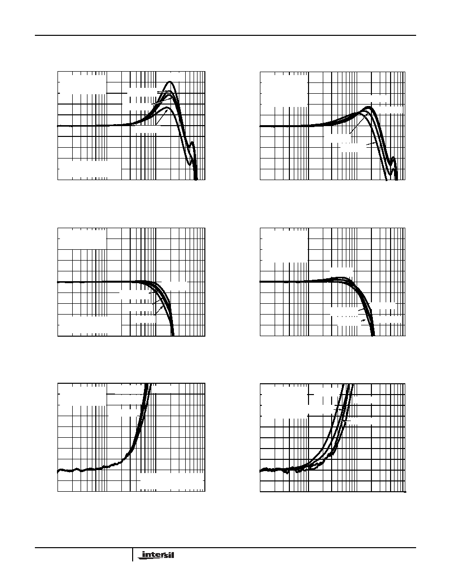
Typical Performance Curves
V
S
=
±
5V, R
L
= 500
to GND, T
A
= 25∞C, unless otherwise specified.
FIGURE 1. SMALL SIGNAL GAIN vs FREQUENCY vs C
L
FIGURE 2. SMALL SIGNAL GAIN vs FREQUENCY vs R
L
FIGURE 3. LARGE SIGNAL GAIN vs FREQUENCY vs C
L
FIGURE 4. LARGE SIGNAL GAIN vs FREQUENCY vs R
L
FIGURE 5. SMALL SIGNAL 0.1dB GAIN vs FREQUENCY vs C
L
FIGURE 6. SMALL SIGNAL 0.1dB GAIN vs FREQUENCY vs R
L
1
10
100
1000
FREQUENCY (MHz)
N
O
RMAL
IZED GAIN
(dB)
C
L
= 1.6pF
A
V
= 1
C
L
INCLUDES 1.6pF
BOARD CAPACITANCE
C
L
= 9.7pF
V
OUT
= 200mV
P-P
-5
-4
-3
-2
-1
0
1
2
3
4
5
R
F
= 332
C
L
= 7.2pF
C
L
= 5.5pF
-5
-4
-3
-2
-1
0
1
2
3
4
5
1
10
100
FREQUENCY (MHz)
NORMALIZED GAIN
(dB)
R
L
= 1k
A
V
= 1
V
OUT
= 200mV
P-P
R
L
= 500
1000
R
L
= 75
C
L
=1.6pF
R
F
= 332
R
L
= 150
1
10
100
1000
FREQUENCY (MHz)
NORMALIZE
D
GAIN
(
d
B
)
C
L
= 7.2pF
C
L
= 1.6pF
C
L
= 5.5pF
C
L
INCLUDES 1.6pF
BOARD CAPACITANCE
C
L
= 9.7pF
-5
-4
-3
-2
-1
0
1
2
3
4
5
A
V
= 2
V
OUT
= 2V
P-P
R
G
= R
F
= 511
-5
-4
-3
-2
-1
0
1
2
3
4
5
1
10
100
FREQUENCY (MHz)
NORMALIZE
D
GAIN (dB
)
R
L
= 1k
R
L
= 500
1000
R
L
= 75
A
V
= 2
V
OUT
= 2V
P-P
C
L
= 5.5pF
R
G
= R
F
= 511
R
L
= 75
R
L
= 150
1
10
100
1000
FREQUENCY (MHz)
N
O
RMAL
IZED GAIN
(dB)
C
L
= 7.2pF
C
L
= 1.6pF
A
V
= 1
C
L
= 5.5pF
C
L
INCLUDES 1.6pF
BOARD CAPACITANCE
C
L
= 9.7pF
V
OUT
= 200mV
P-P
R
F
= 332
-0.2
-0.1
0
0.1
0.2
0.3
0.4
0.5
0.6
0.7
0.8
-0.2
-0.1
0
0.1
0.2
0.3
0.4
0.5
0.6
0.7
0.8
1
10
100
FREQUENCY (MHz)
NOR
M
ALIZED GAIN
(dB)
R
L
= 1k
R
L
= 150
A
V
= 1
V
OUT
= 200mV
P-P
1000
R
L
= 75
C
L
= 1.6pF
R
F
= 332
R
L
= 500
ISL59440

5
FN6162.1
September 21, 2005
FIGURE 7. LARGE SIGNAL 0.1dB GAIN vs FREQUENCY vs C
L
FIGURE 8. LARGE SIGNAL 0.1dB GAIN vs FREQUENCY vs R
L
FIGURE 9. PSRR
CHANNELS
FIGURE 10. CROSSTALK
AND OFF ISOLATION
FIGURE 11. INPUT NOISE vs FREQUENCY
FIGURE 12. INPUT NOISE vs FREQUENCY
Typical Performance Curves
V
S
=
±
5V, R
L
= 500
to GND, T
A
= 25∞C, unless otherwise specified. (Continued)
1
10
100
1000
FREQUENCY (MHz)
NORMALIZE
D
GAIN (dB
)
C
L
= 1.6pF
C
L
INCLUDES 1.6pF
BOARD CAPACITANCE
C
L
= 9.7pF
-0.8
-0.7
-0.6
-0.5
-0.4
-0.3
-0.2
-0.1
0
0.1
0.2
A
V
= 2
V
OUT
= 2V
P-P
R
G
= R
F
= 511
C
L
= 7.2pF
C
L
= 5.5pF
-0.5
-0.4
-0.3
-0.2
-0.1
0
0.1
0.2
0.3
0.4
0.5
1
10
100
FREQUENCY (MHz)
NOR
M
ALIZED GAIN
(dB)
R
L
= 1k
1000
R
L
= 75
A
V
= 2
V
OUT
= 2V
P-P
C
L
= 5.5pF
R
G
= R
F
= 511
R
L
= 150
R
L
= 500
FREQUENCY (MHz)
0
-10
-30
PSRR (dB)
0.3
1
10
100
1000
-50
-70
PSRR (V-)
PSRR (V+)
10
-20
-40
-60
-80
20
A
V
= 2
V
IN
= 200mV
P-P
C
L
= 5.5pF
R
G
= R
F
= 511
FREQUENCY (MHz)
-20
-40
-60
(dB
)
0.001
0.1
10
100
500
-80
-100
CROSSTALK
OFF ISOLATION
-30
-50
-70
-90
-110
-10
1
0.01
3 6
A
V
= 2
V
IN
= 1
V
P-P
C
L
= 5.5pF
R
G
= R
F
= 511
0.1
1
10
100
FREQUENCY (kHz)
A
V
= 1, R
F
= 500
24
20
16
12
8
4
0
-I
IN
C
URRENT NOISE (p
A/
Hz
)
60
50
40
30
20
10
0
0.1
1
10
100
FREQUENCY (kHz)
I
N
P
U
T VO
L
T
AGE NOI
SE (n
V/
Hz
)
A
V
= 1, R
F
= 500
ISL59440