 | –≠–ª–µ–∫—Ç—Ä–æ–Ω–Ω—ã–π –∫–æ–º–ø–æ–Ω–µ–Ω—Ç: ISL5961IA | –°–∫–∞—á–∞—Ç—å:  PDF PDF  ZIP ZIP |
TM
1
File Number 6007.2
ISL5961
14-Bit, +3.3V, 130/210+MSPS,
CommLink
TM
High Speed D/A Converter
The ISL5961 is a 14-bit,
130/210+MSPS (Mega Samples
Per Second), CMOS, high speed,
low power, D/A (digital to analog) converter, designed
specifically for use in high performance communication
systems such as base transceiver stations utilizing 2.5G or
3G cellular protocols.
This device complements the CommLink ISL5x61 family of
high speed converters, which include 10, 12, and 14-bit
devices.
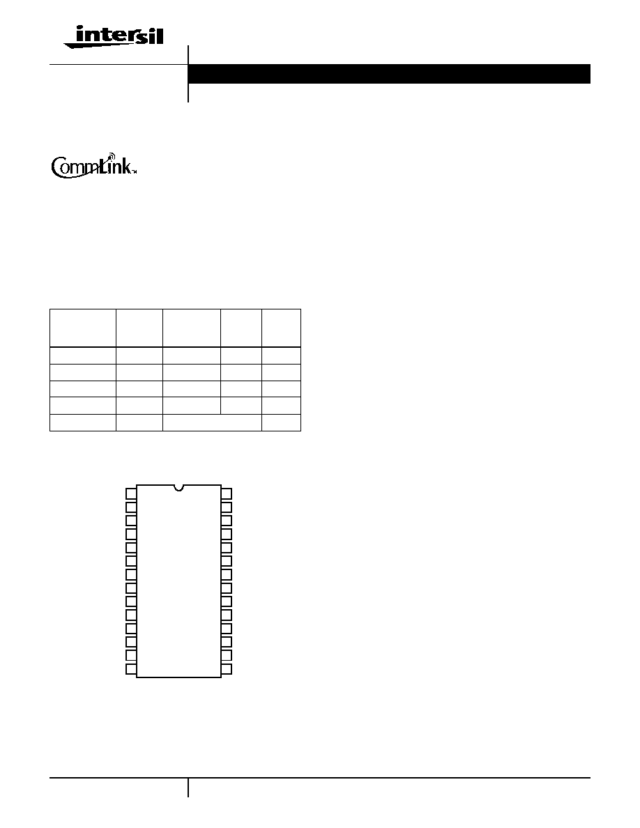
Pinout
ISL5961
TOP VIEW
Features
∑ Speed Grades . . . . . . . . . . . . . . . . 130M and 210+MSPS
∑ Low Power . . . . . 103mW with 20mA Output at 130MSPS
∑ Adjustable Full Scale Output Current. . . . . 2mA to 20mA
∑ +3.3V Power Supply
∑ 3V LVCMOS Compatible Inputs
∑ Excellent Spurious Free Dynamic Range
(75dBc to Nyquist, f
S
= 130MSPS, f
OUT
= 10MHz)
∑ UMTS Adjacent Channel Power =71dB at 19.2MHz
∑ EDGE/GSM SFDR = 94dBc at 11MHz in 20MHz Window
∑ Pin compatible, 3.3V, Lower Power Replacement For The
AD9754 and HI5960
Applications
∑ Cellular Infrastructure - Single or Multi-Carrier: IS-136, IS-
95, GSM, EDGE, CDMA2000, WCDMA, TDS-CDMA
∑ BWA Infrastructure
∑ Medical/Test Instrumentation
∑ Wireless Communication Systems
∑ High Resolution Imaging Systems
∑ Arbitrary Waveform Generators
Ordering Information
PART
NUMBER
TEMP.
RANGE
(
o
C)
PACKAGE
PKG.
NO.
CLOCK
SPEED
ISL5961IB
-40 to 85 28 Ld SOIC
M28.3
130MHz
ISL5961IA
-40 to 85 28 Ld TSSOP M28.173 130MHz
ISL5961/2IB
-40 to 85 28 Ld SOIC
M28.3
210MHz
ISL5961/2IA
-40 to 85 28 Ld TSSOP M28.173 210MHz
ISL5961EVAL1
25
SOIC Evaluation Platform 210MHz
28
27
26
25
24
23
22
21
20
19
18
17
16
15
D13 (MSB)
D12
D11
D10
D9
D8
D7
D6
D5
D4
D3
D2
D1
D0 (LSB)
1
2
3
4
5
6
7
8
9
10
11
12
13
14
CLK
DCOM
NC
AV
DD
COMP
IOUTB
NC
FSADJ
REFIO
REFLO
SLEEP
DV
DD
IOUTA
ACOM
Data Sheet
September 2001
CAUTION: These devices are sensitive to electrostatic discharge; follow proper IC Handling Procedures.
1-888-INTERSIL or 321-724-7143
|
Intersil and Design is a trademark of Intersil Americas Inc.
Copyright © Intersil Americas Inc. 2001, All Rights Reserved
CommLinkTM is a trademark of Intersil Americas Inc.

2
Typical Applications Circuit
Functional Block Diagram
D11 (3)
D10 (4)
D9 (5)
D8 (6)
D7 (7)
D6 (8)
D5 (9)
D4 (10)
D11
D10
D9
D8
D7
D6
D5
D4
DCOM (26)
CLK (28)
(24) AV
DD
(22) IOUTA
(21) IOUTB
(18) FSADJ
(16) REFLO
ISL5961
DV
DD
(27)
0.1
µF
10
µF
(20) ACOM
50
(15) SLEEP
(17) REFIO
0.1
µF
1.91k
FERRITE
10
µH
(23) COMP
0.1
µF
+
BEAD
R
SET
D3
D2
D1
D0
D3 (11)
D2 (12)
D1 (13)
D0 (LSB) (14)
0.1
µF
10
µH
+
BEAD
(25, 19) NC
ACOM
DCOM
10
µF
D13 (1)
D12 (2)
D13
D12
+3.3V (V
DD
)
50
(50
)
1:1, Z1:Z2
ONE CONNECTION
ANY 50
LOAD
REPRESENTS
UPPER
VOLTAGE
REFERENCE
(LSB) D0
D1
D2
D3
D4
D5
D6
D9
CLK
D7
D8
5-BIT
DECODER
REFIO
CASCODE
CURRENT
SOURCE
SWITCH
MATRIX
BIAS
GENERATION
INT/EXT
40
40
31 MSB
SEGMENTS
9 LSBs
+
COMP
IOUTA
IOUTB
D10
D11
D12
(MSB) D13
INPUT
LATCH
REFLO
FSADJ SLEEP
ISL5961

3
Pin Descriptions
PIN NO.
PIN NAME
DESCRIPTION
1-14
D13 (MSB) Through
D0 (LSB)
Digital Data Bit 13, (Most Significant Bit) through Digital Data Bit 0, (Least Significant Bit).
15
SLEEP
Control Pin for Power-Down mode. Sleep Mode is active high; Connect to ground for Normal Mode. Sleep pin
has internal 20
µA active pulldown current.
16
REFLO
Connect to analog ground to enable internal 1.2V reference or connect to AV
DD
to disable internal reference.
17
REFIO
Reference voltage input if internal reference is disabled. Reference voltage output if internal reference is
enabled. Use 0.
1µF cap to ground when internal reference is enabled.
18
FSADJ
Full Scale Current Adjust. Use a resistor to ground to adjust full scale output current. Full Scale Output
Current = 32 x V
FSADJ
/R
SET
.
19, 25
NC
No Connect. These should be grounded, but can be left disconnected.
21
IOUTB
The complementary current output of the device. Full scale output current is achieved when all input bits are
set to binary 0.
22
IOUTA
Current output of the device. Full scale output current is achieved when all input bits are set to binary 1.
23
COMP
Connect 0.1
µF capacitor to ACOM.
24
AV
DD
Analog Supply (+2.7V to +3.6V).
20
ACOM
Connect to Analog Ground.
26
DCOM
Connect to Digital Ground.
27
DV
DD
Digital Supply (+2.7V to +3.6V).
28
CLK
Clock Input.
ISL5961

4
Absolute Maximum Ratings
Thermal Information
Digital Supply Voltage DV
DD
to DCOM . . . . . . . . . . . . . . . . . +3.6V
Analog Supply Voltage AV
DD
to ACOM . . . . . . . . . . . . . . . . . +3.6V
Grounds, ACOM TO DCOM . . . . . . . . . . . . . . . . . . . -0.3V to +0.3V
Digital Input Voltages (D9-D0, CLK, SLEEP). . . . . . . . DV
DD
+ 0.3V
Reference Input Voltage Range. . . . . . . . . . . . . . . . . . AV
DD
+ 0.3V
Analog Output Current (I
OUT
) . . . . . . . . . . . . . . . . . . . . . . . . . 24mA
Operating Conditions
Temperature Range. . . . . . . . . . . . . . . . . . . . . . . . . . -40
o
C to 85
o
C
Thermal Resistance (Typical, Note 1)
JA
(
o
C/W)
SOIC Package . . . . . . . . . . . . . . . . . . . . . . . . . . . . .
75
TSSOP Package . . . . . . . . . . . . . . . . . . . . . . . . . . .
110
Maximum Junction Temperature . . . . . . . . . . . . . . . . . . . . . . . 150
o
C
Maximum Storage Temperature Range . . . . . . . . . -65
o
C to 150
o
C
Maximum Lead Temperature (Soldering 10s) . . . . . . . . . . . . . 300
o
C
(SOIC - Lead Tips Only)
CAUTION: Stresses above those listed in "Absolute Maximum Ratings" may cause permanent damage to the device. This is a stress only rating and operation of the
device at these or any other conditions above those indicated in the operational sections of this specification is not implied.
NOTE:
1.
JA
is measured with the component mounted on an evaluation PC board in free air.
Electrical Specifications
AV
DD
= DV
DD
= +3.3V, V
REF
= Internal 1.2V, IOUTFS = 20mA, T
A
= 25
o
C for All Typical Values
PARAMETER
TEST CONDITIONS
T
A
= -40
o
C TO 85
o
C
UNITS
MIN
TYP
MAX
SYSTEM PERFORMANCE
Resolution
14
-
-
Bits
Integral Linearity Error, INL
"Best Fit" Straight Line (Note 7)
-5
±2.5
+5
LSB
Differential Linearity Error, DNL
(Note 7)
-3
±1.5
+3
LSB
Offset Error, I
OS
IOUTA (Note 7)
-0.006
+0.006
% FSR
Offset Drift Coefficient
(Note 7)
-
0.1
-
ppm
FSR/
o
C
Full Scale Gain Error, FSE
With External Reference (Notes 2, 7)
-3
±0.5
+3
% FSR
With Internal Reference (Notes 2, 7)
-3
±0.5
+3
% FSR
Full Scale Gain Drift
With External Reference (Note 7)
-
±50
-
ppm
FSR/
o
C
With Internal Reference (Note 7)
-
±100
-
ppm
FSR/
o
C
Full Scale Output Current, I
FS
2
-
20
mA
Output Voltage Compliance Range
(Note 3)
-1.0
-
1.25
V
DYNAMIC CHARACTERISTICS
Maximum Clock Rate, f
CLK
ISL5961/2IA, ISL5961/2IB
210
250
-
MHz
Maximum Clock Rate, f
CLK
ISL5961IA, ISL5961IB
130
150
-
MHz
Output Rise Time
Full Scale Step
-
1.5
-
ns
Output Fall Time
Full Scale Step
-
1.5
-
ns
Output Capacitance
-
10
-
pF
Output Noise
IOUTFS = 20mA
-
50
-
pA/
Hz
IOUTFS = 2mA
-
30
-
pA/
Hz
AC CHARACTERISTICS (Using Figure 13 with R
DIFF
= 50
and R
LOAD
= 50
, Full Scale Output = -2.5dBm)
Spurious Free Dynamic Range,
SFDR Within a Window
f
CLK
= 210MSPS, f
OUT
= 80.8MHz, 30MHz Span (Notes 4, 7)
-
73
-
dBc
f
CLK
= 210MSPS, f
OUT
= 40.4MHz, 30MHz Span (Notes 4, 7)
-
82
-
dBc
f
CLK
= 130MSPS, f
OUT
= 20.2MHz, 20MHz Span (Notes 4, 7)
-
86
-
dBc
ISL5961

5
Spurious Free Dynamic Range,
SFDR to Nyquist (f
CLK
/2)
f
CLK
= 210MSPS, f
OUT
= 80.8MHz (Notes 4, 7)
-
52
-
dBc
f
CLK
= 210MSPS, f
OUT
= 40.4MHz (Notes 4, 7, 9)
-
61
-
dBc
f
CLK
= 200MSPS, f
OUT
= 20.2MHz, T = 25
o
C (Notes 4, 7)
62
64
-
dBc
f
CLK
= 200MSPS, f
OUT
= 20.2MHz, T = -40
o
C to 85
o
C (Notes 4, 7)
60
-
-
dBc
f
CLK
= 130MSPS, f
OUT
= 50.5MHz (Notes 4, 7)
-
59
-
dBc
f
CLK
= 130MSPS, f
OUT
= 40.4MHz (Notes 4, 7)
-
63
-
dBc
f
CLK
= 130MSPS, f
OUT
= 20.2MHz (Notes 4, 7)
-
70
-
dBc
f
CLK
= 130MSPS, f
OUT
= 10.1MHz (Notes 4, 7)
-
75
-
dBc
f
CLK
= 130MSPS, f
OUT
= 5.05MHz, T = 25
o
C (Notes 4, 7)
72
79
-
dBc
f
CLK
= 130MSPS, f
OUT
= 5.05MHz, T = -40
o
C to 85
o
C (Notes 4, 7)
70
-
-
dBc
f
CLK
= 100MSPS, f
OUT
= 40.4MHz (Notes 4, 7)
-
61
-
dBc
f
CLK
= 80MSPS, f
OUT
= 30.3MHz (Notes 4, 7)
-
65
-
dBc
f
CLK
= 80MSPS, f
OUT
= 20.2MHz (Notes 4, 7)
-
71
-
dBc
f
CLK
= 80MSPS, f
OUT
= 10.1MHz (Notes 4, 7, 9)
-
71
-
dBc
f
CLK
= 80MSPS, f
OUT
= 5.05MHz (Notes 4, 7)
-
78
-
dBc
f
CLK
= 50MSPS, f
OUT
= 20.2MHz (Notes 4, 7)
-
70
-
dBc
f
CLK
= 50MSPS, f
OUT
= 10.1MHz (Notes 4, 7)
-
75
-
dBc
f
CLK
= 50MSPS, f
OUT
= 5.05MHz (Notes 4, 7)
-
79
-
dBc
Spurious Free Dynamic Range,
SFDR in a Window with Eight Tones
f
CLK
= 210MSPS, f
OUT
= 28.3MHz to 45.2MHz, 2.1MHz Spacing,
50MHz Span (Notes 4, 7, 9)
-
67
-
dBc
f
CLK
= 130MSPS, f
OUT
=17.5MHz to 27.9MHz, 1.3MHz Spacing,
35MHz Span (Notes 4, 7)
-
70
-
dBc
f
CLK
= 80MSPS, f
OUT
= 10.8MHz to 17.2MHz, 811kHz Spacing,
15MHz Span (Notes 4, 7)
-
77
-
dBc
f
CLK
= 50MSPS, f
OUT
= 6.7MHz to 10.8MHz, 490kHz Spacing,
10MHz Span (Notes 4, 7)
-
78
-
dBc
Spurious Free Dynamic Range,
SFDR in a Window with EDGE or GSM
f
CLK
= 78MSPS, f
OUT
= 11MHz, in a 20MHz Window, RBW=30kHz
(Notes 4, 7, 9)
-
94
-
dBc
Adjacent Channel Power Ratio,
ACPR with UMTS
f
CLK
= 76.8MSPS, f
OUT
= 19.2MHz, RBW=30kHz (Notes 4, 7, 9)
-
71
-
dB
VOLTAGE REFERENCE
Internal Reference Voltage, V
FSADJ
Pin 18 Voltage with Internal Reference
1.2
1.23
1.3
V
Internal Reference Voltage Drift
-
±40
-
ppm/
o
C
Internal Reference Output Current
Sink/Source Capability
Reference is not intended to be externally loaded
-
0
-
µA
Reference Input Impedance
-
1
-
M
Reference Input Multiplying Bandwidth (Note 7)
-
1.0
-
MHz
DIGITAL INPUTS D13-D0, CLK
Input Logic High Voltage with
3.3V Supply, V
IH
(Note 3)
2.3
3.3
-
V
Input Logic Low Voltage with
3.3V Supply, V
IL
(Note 3)
-
0
1.0
V
Sleep Input Current, I
IH
-25
-
+25
µA
Electrical Specifications
AV
DD
= DV
DD
= +3.3V, V
REF
= Internal 1.2V, IOUTFS = 20mA, T
A
= 25
o
C for All Typical Values (Continued)
PARAMETER
TEST CONDITIONS
T
A
= -40
o
C TO 85
o
C
UNITS
MIN
TYP
MAX
ISL5961