1
Æ
FN8087.1
CAUTION: These devices are sensitive to electrostatic discharge; follow proper IC Handling Procedures.
1-888-INTERSIL or 321-724-7143
|
Intersil (and design) is a registered trademark of Intersil Americas Inc.
Copyright Intersil Americas Inc. 2004-2005. All Rights Reserved
All other trademarks mentioned are the property of their respective owners.
ISL60007
Precision 1.25V and 2.50V, 1.08µ-Watt,
High Precision FGATM Voltage References
The ISL60007 FGATM voltage references are extremely low
power, very high precision analog voltage references
fabricated in Intersil's proprietary Floating Gate Analog
technology. The ISL60007 features low supply voltage
operation at ultra-low 400nA operating current resulting in
typical 1.08µW power consumption.
In addition, the ISL60007 family features guaranteed initial
accuracy as low as ±0.5mV, temperature coefficients as tight
as 3ppm/∞C and long-term stability of 10ppm/
1kHrs.
The initial accuracy and thermal stability performance of the
ISL60007 family plus the low power consumption eliminates
the need to compromise accuracy and thermal stability for
reduced power consumption making it an ideal high
resolution, low power data conversion system.
Pinout
ISL60007 (8 LD SOIC)
TOP VIEW
Features
∑ Reference Voltage . . . . . . . . . . . . . . . . . 1.25V, and 2.50V
∑ Absolute Initial Accuracy Options. . . . . ±0.5mV, & ±1.0mV
∑ 1.08µW typical Power Consumption
∑ Supply Voltage Range . . . . . . . . . . . . . . . . . . 2.7V to 5.5V
∑ Ultra-Low Supply Current. . . . . . . . . . . . . . . . . . . . .400nA
∑ Low Temperature Coefficient Options . . . . . . . . . 3ppm/∞C
5ppm/∞C, & 10ppm/∞C
∑ Long Term Stability. . . . . . . . . . . . . . . . . . . 10ppm/
1kHrs
∑ 7mA Source & Sink Current
∑ ESD Protection. . . . . . . . . . . . . 5kV (Human Body Model)
∑ Standard 8 Ld SOIC Packaging
∑ Temperature Range . . . . . . . . . . . . . . . . . .-40∞C to +85∞C
Applications
∑ High Resolution A/Ds & D/As
∑ Digital Meters
∑ Bar Code Scanners
∑ Mobile Communications
∑ PDA's and Notebooks
∑ Battery Management Systems
∑ Medical Systems
Typical Application
Ordering Information
PART NUMBER
TEMP.
RANGE (∞C) PACKAGE GRADE
V
OUT
OPTION
ISL60007CIB812
-40 to +85
8 Ld SOIC
±0.5mV,
5ppm/∞C
1.250V
ISL60007DIB812
-40 to +85
8 Ld SOIC
±1.0mV,
10ppm/∞C
1.250V
ISL60007BIB825
-40 to +85
8 Ld SOIC ±0.5mV,
3ppm/∞C
2.500V
ISL60007CIB825
-40 to +85
8 Ld SOIC ±0.5mV,
5ppm/∞C
2.500V
ISL60007DIB825
-40 to +85
8 Ld SOIC ±1.0mV,
10ppm/∞C
2.500V
Pin Descriptions
PIN NAME
DESCRIPTION
GND
Ground Connection
V
IN
Power Supply Input Connection
V
OUT
Voltage Reference Output Connection
DNC
Do Not Connect; Internal Connection -
Must Be Left Floating
1
2
3
4
8
7
6
5
V
IN
DNC
GND
DNC
DNC
V
OUT
DNC
GND
V
IN
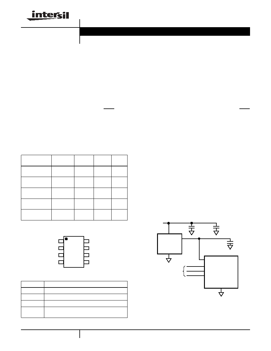
= +3.0V
0.1µF
0.001µF*
SERIAL
BUS
V
IN
V
OUT
GND
ISL60007
ENABLE
SCK
SDAT
A/D CONVERTER
16 TO 24-BIT
REF IN
10µF
*Also see Figure 29 in Applications Information.
Data Sheet
May 5, 2005

2
FN8087.1
May 5, 2005
Absolute Maximum Ratings
Recommended Operating Conditions
Storage Temperature Range . . . . . . . . . . . . . . . . . .-65∞C to +125∞C
Max Voltage V
IN
to Gnd. . . . . . . . . . . . . . . . . . . . . . . -0.5V to +6.5V
Max Voltage V
OUT
to Gnd (10s) . . . . . . . . . . . . . . . -0.5V to +3.50V
Voltage on "DNC" pins . . . . No connections permitted to these pins.
Lead Temperature, soldering (10s) . . . . . . . . . . . . . . . . . . . . +225∞C
Temperature Range (Industrial) . . . . . . . . . . . . . . . . . . -40∞C to 85∞C
CAUTION: Stresses above those listed in "Absolute Maximum Ratings" may cause permanent damage to the device. This is a stress only rating and operation of the
device at these or any other conditions above those indicated in the operational sections of this specification is not implied.
Electrical Specifications
Operating Conditions: V
IN
= 3.0V, I
OUT
= 0mA, C
OUT
= 0.001µF, T
A
= -40 to +85∞C, Unless Otherwise
Specified.
SYMBOL
PARAMETER
CONDITIONS
MIN
TYP
MAX
UNITS
1.250V OUTPUT VOLTAGE
V
OUT
Output Voltage
1.250
V
V
OA
V
OUT
Accuracy @ T
A
= 25∞C
ISL60007C12
-0.5
+0.5
mV
ISL60007D12
-1.0
+1.0
mV
TC V
OUT
Output Voltage Temperature
Coefficient (Note 1)
ISL60007C12
5
ppm/∞C
ISL60007D12
10
ppm/∞C
V
IN
Input Voltage Range
2.7
5.5
V
I
IN
Supply Current
400
800
nA
V
OUT
/
V
IN
Line Regulation
+2.7V
V
IN
+5.5V
30
200
µV/V
V
OUT
/
I
OUT
Load Regulation
Sourcing: 0mA
I
OUT
7mA
15
50
µV/mA
Sinking: -7mA
I
OUT
0mA
50
150
µV/mA
V
OUT
/
t
Long Term Stability
T
A
= 25∞C
10
ppm/
1kHrs
V
OUT
/
T
A
Thermal Hysteresis (Note 2)
T
A
= 125∞C
50
ppm
I
SC
Short Circuit Current (Note 3)
T
A
= 25∞C
40
80
mA
V
N
V
OUT
Noise
0.1Hz
f 10Hz
30
µV
P-P
2.500V OUTPUT VOLTAGE
V
OUT
Output Voltage
2.500
V
V
OA
V
OUT
Accuracy @
T
A
= 25∞C
ISL60007B25
-0.5
+0.5
mV
ISL60007C25
-0.5
+0.5
mV
ISL60007D25
-1.0
+1.0
mV
TC V
OUT
Output Voltage Temperature
Coefficient (Note 1)
ISL60007B25
3
ppm/∞C
ISL60007C25
5
ppm/∞C
ISL60007D25
10
ppm/∞C
V
IN
Input Voltage Range
2.7
5.5
V
I
IN
Supply Current
400
800
nA
V
OUT
/
V
IN
Line Regulation
+2.7V
V
IN
+5.5V
30
200
µV/V
V
OUT
/
I
OUT
Load Regulation
Sourcing: 0mA
I
OUT
7mA
15
50
µV/mA
Sinking: -7mA
I
OUT
0mA
50
150
µV/mA
V
OUT
/
t
Long Term Stability (Note 4)
T
A
= 25∞C
10
ppm/
1kHrs
V
OUT
/
T
A
Thermal Hysteresis (Note 2)
T
A
= 125∞C
50
ppm
ISL60007

3
FN8087.1
May 5, 2005
I
SC
Short Circuit Current (Note 3)
T
A
= 25∞C, V
OUT
tied to Gnd
40
80
mA
V
N
Output Voltage Noise
0.1Hz
f 10Hz
30
µV
p-p
NOTES:
1. Over the specified temperature range. Temperature coefficient is measured by the box method whereby the change in V
OUT
is divided by the
temperature range; in this case, -40∞C to +85∞C = 125∞C.
2. Thermal Hysteresis is the change in V
OUT
measured @ T
A
= 25∞C after temperature cycling over a specified range,
T
A
. V
OUT
is read initially
at T
A
= 25∞C for the device under test. The device is temperature cycled and a second V
OUT
measurement is taken at 25∞C. The difference
between the initial V
OUT
reading and the second V
OUT
reading is then expressed in ppm. For
T
A
= 125∞C, the device under test is cycled
from +25∞C to +85∞C to -40∞C to +25∞C.
3. Guaranteed by device characterization and/or correlation to other device tests.
4. FGA voltage reference long term drift is a logarithmic characteristic. Changes that occur after the first few hundred hours of operation are
significantly smaller with time, asymptotically approaching zero beyond 1000 hours. Because of this decreasing characteristic, long term drift is
specified in ppm/
1kHrs.
Electrical Specifications
Operating Conditions: V
IN
= 3.0V, I
OUT
= 0mA, C
OUT
= 0.001µF, T
A
= -40 to +85∞C, Unless Otherwise
Specified. (Continued)
SYMBOL
PARAMETER
CONDITIONS
MIN
TYP
MAX
UNITS
Typical Performance Curves, 1.25V Reference
V
IN
= 3.0V, I
OUT
= 0mA, T
A
= 25∞C
Unless Otherwise Specified
FIGURE 1. I
IN
vs V
IN
- 3 UNITS
FIGURE 2. I
IN
vs V
IN
- 3 TEMPS
100
200
300
400
500
600
2.7
3.4
4.1
4.8
5.5
V
IN
(V)
I
IN
(nA)
440nA
330nA
240nA
250
300
350
400
2.7
3.4
4.1
4.8
5.5
-40∞C
+25∞C
+85∞C
V
IN
(V)
I
IN
(nA)
ISL60007

4
FN8087.1
May 5, 2005
FIGURE 3. V
OUT
vs TEMPERATURE NORMALIZED TO 25∞C
FIGURE 4. LINE REGULATION - 3 UNITS
FIGURE 5. LINE REGULATION - 3 TEMPS
FIGURE 6. LINE TRANSIENT RESPONSE, C
L
= 0nF
FIGURE 7. LINE TRANSIENT RESPONSE, C
L
= 1nF
FIGURE 8. PSRR vs f vs C
L
Typical Performance Curves, 1.25V Reference
V
IN
= 3.0V, I
OUT
= 0mA, T
A
= 25∞C
Unless Otherwise Specified (Continued)
1.249
1.2492
1.2494
1.2496
1.2498
1.25
1.2502
1.2504
1.2506
1.2508
-40
-15
10
35
60
85
TEMPERATURE (∞C)
V
OU
T
(V)
UNIT 1
UNIT 2
UNIT 3
1.24996
1.24997
1.24998
1.24999
1.25
1.25001
1.25002
1.25003
1.25004
1.25005
1.25006
2.7
3.4
4.1
4.8
5.5
V
IN
(V)
V
OU
T
(
V
)
(N
OR
MA
L
I
Z
E
D
T
O
1
.
25
V A
T
V
IN
=3
V
)
440nA
240nA
330nA
-50
-25
0
25
50
2.7
3.4
4.1
4.8
5.5
V
IN
DEL
T
A V
OU
T
(µV)
(NO
R
MA
LI
ZED T
O
V
I
N = 3.0
V
)
+85∞C
-40∞C
+25∞C
5
0
m
V
/DIV
500µs/DIV
V
IN
= +0.3V
V
IN
= -0.3V
50m
V/DI
V
500µs/DIV
V
IN
= +0.3V
V
IN
= -0.3V
-100
-90
-80
-70
-60
-50
-40
-30
-20
-10
0
1
10
100
1000
10000
100000
1000000
FREQUENCY (Hz)
PSRR (dB)
C
L
= 100nF
C
L
= 10nF
C
L
= 0nF
C
L
= 1nF
ISL60007

5
FN8087.1
May 5, 2005
FIGURE 9. LOAD REGULATION vs TEMP
FIGURE 10. LOAD TRANSIENT RESPONSE @ I
L
=50µA, C
L
=1nF
FIGURE 11. LOAD TRANSIENT RESPONSE @ I
L
=7mA, C
L
=1nF
FIGURE 12. TURN-ON TIME @ T
A
= 25∞C
Typical Performance Curves, 1.25V Reference
V
IN
= 3.0V, I
OUT
= 0mA, T
A
= 25∞C
Unless Otherwise Specified (Continued)
-0.20
-0.10
0.00
0.10
0.20
0.30
0.40
-7
-6
-5
-4
-3
-2
-1
0
1
2
3
4
5
6
7
SINKING
OUTPUT CURRENT (mA)
SOURCING
DEL
T
A V
(mV)
+85∞C
+25∞C
-40∞C
50mV
/
DI
V
200µs/DIV
I
L
= +50µA
I
L
= -50µA
2
0
0
m
V
/DIV
500µs/DIV
I
L
= +7mA
I
L
= -7mA
0
0.5
1
1.5
2
2.5
3
3.5
0
2
4
6
8
10
12
TIME (ms)
V
IN
V
OUT
V
IN
AND
V
OU
T
(V)
Typical Performance Curves, 2.5V Reference
V
IN
= 3.0V, I
OUT
= 0mA, T
A
= 25∞C
Unless Otherwise Specified
FIGURE 13. I
IN
vs V
IN
- 3 UNITS
FIGURE 14. I
IN
vs V
IN
- 3 TEMPS
100
200
300
400
500
600
700
800
2.7
3.4
4.1
4.8
5.5
V
IN
(V)
I
IN
(nA)
250nA
400nA
570nA
300
350
400
450
500
2.7
3.4
4.1
4.8
5.5
V
IN
(V)
I
IN
(nA)
-40∞C
+25∞C
+85∞C
ISL60007