
1
Æ
FN9005.4
ISL6123, ISL6124, ISL6125,
ISL6126, ISL6127, ISL6128
Power Sequencing Controllers
The Intersil ISL6123, ISL6124, ISL6125, ISL6126, ISL6127,
ISL6128 are integrated 4 channel controlled-on/controlled-
off power-supply sequencers with supply monitoring, fault
protection and a "sequence completed" signal (RESET#).
For larger systems, more than 4 supplies can be sequenced
by simply connecting a wire between SYSRESET# pins of
cascaded IC's. The ISL6125 uses 4 open-drain outputs to
control the 4 power supplies, and the other sequencers use
a patented, micropower 7X chargepump to drive 4 external
low-cost NFET switch gates above the supply rail by 5.3V.
These IC's can be biased from any supply 5V down to 1.5V.
Individual product descriptions are below.
The four channel ISL6123 (ENABLE input), ISL6124
(ENABLE# input) and ISL6125 ICs offer the designer 4 rail
control when it is required that all four rails are in minimal
compliance prior to turn on and that compliance must be
maintained during operation. The ISL6123 has a low power
standby mode when it is disabled, suitable for battery
powered applications.
The ISL6125 operates like the ISL6124 but instead of
charge pump driven gate drive outputs it has open drain
logic outputs for direct interface to other circuitry.
In contrast to the ISL6123 and ISL6124, with the ISL6126,
each of the four channels operates independently so that the
various rails will turn on once its individual input voltage
requirements are met.
The ISL6127 is a preprogrammed A-B-C-D turn-on and D-C-
B-A turn-off sequenced IC. Once all inputs are in compliance
and ENABLE is asserted the sequencing starts and each
subsequent GATE will turn-on after the previous one
completes turning-on.
The ISL6128 has two groups of two channels each with its
independent I/O and is ideal for voltage sequencing into
redundant capability loads as all four inputs need to be
satisfied prior to turn on but a single group fault is ignored by
the other group.
External resistors provide flexible voltage threshold
programming of monitored rail voltages. Delay and
sequencing are provided by external capacitors for both
ramp up and ramp down.
Additional I/O is provided indicating and driving RESET state
in various configurations.
For volume applications, other programmable options and
features can be had. Contact the factory with your needs.
Features
∑ Enables arbitrary turn-on and turn-off sequencing of up to
four power supplies (0.7V - 5V)
∑ Operates from 1.5V to 5V supply voltage
∑ Supplies V
DD
+5.3V of charge pumped gate drive
∑ Adjustable voltage slew rate for each rail
∑ Multiple sequencers can be daisy-chained to sequence an
infinite number of independent supplies
∑ Glitch immunity
∑ Under voltage lockout for each supply
∑ 1µA Sleep State (ISL6123)
∑ Active high (ISL6123) or low (ISL6124) ENABLE# input
∑ Open drain version available (ISL6125)
∑ Pre programmed Sequence available (ISL6127)
∑ Dual channel groupings (ISL6128)
∑ QFN Package with Pb-free plus anneal option
Applications
∑ Graphics cards
∑ FPGA/ASIC/microprocessor/PowerPC supply sequencing
∑ Network routers
∑ Telecommunications systems
Ordering Information
PART NUMBER
TEMP.
RANGE (∞C)
PACKAGE
PKG.
DWG. #
ISL6123IR
-40 to +85
24 Ld 4x4 QFN
L24.4x4
ISL6124IR
ISL6125IR
ISL6126IR
ISL6127IR
ISL6128IR
ISL6123IRZA (Note)
-40 to +85
24 Ld 4x4 QFN
(Pb-free)
ISL6124IRZA (Note)
ISL6125IRZA (Note)
ISL6126IRZA (Note)
ISL6127IRZA (Note)
ISL6128IRZA (Note)
ISL612XSEQEVAL1
Evaluation Platform
NOTE: Intersil Pb-free plus anneal products employ special Pb-free
material sets; molding compounds/die attach materials and 100% matte
tin plate termination finish, which are RoHS compliant and compatible
with both SnPb and Pb-free soldering operations. Intersil Pb-free
products are MSL classified at Pb-free peak reflow temperatures that
meet or exceed the Pb-free requirements of IPC/JEDEC J STD-020.
Data Sheet
June 10, 2005
CAUTION: These devices are sensitive to electrostatic discharge; follow proper IC Handling Procedures.
1-888-INTERSIL or 1-888-468-3774
|
Intersil (and design) is a registered trademark of Intersil Americas Inc.
Copyright Intersil Americas Inc.2001, 2003, 2004 All Rights Reserved.
All other trademarks mentioned are the property of their respective owners.
2
FN9005.4
June 10, 2005
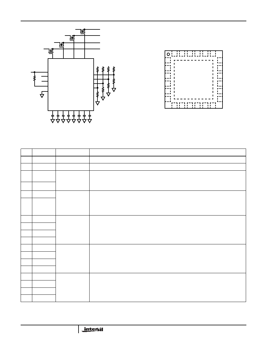
Pinout
ISL6123, ISL6124, ISL6125,
ISL6126, ISL6127, ISL6128 (QFN)
TOP VIEW
FIGURE 1. TYPICAL ISL6123 APPLICATION USAGE
AOUT
AIN
BIN
CIN
DIN
BOUT
COUT
DOUT
UVLO_B
UVLO_A
UVLO_D
UVLO_C
A
IN
DLY
_
O
N
_
A
DLY_O
FF_A
DLY_
O
FF_
B
DLY_
O
FF_
C
DLY_
O
FF_
D
DLY
_
O
N
_
B
DLY
_
O
N
_
C
DLY
_
O
N
_
D
ENABLE
SYSRST#
GROUND
BIN
CIN
DIN
RESET#
V
DD
GATE D
GATE C
GATE B
GATE A
4mm X 4mm
1
2
3
4
5
6
18
17
16
15
14
13
24
23
22
21
20
19
7
8
9
10
11
12
Pin Descriptions
PIN #
PIN NAME
FUNCTION
DESCRIPTION
23
VDD
Chip Bias
Bias IC from nominal 1.5V to 5V
10
GND
Bias Return
IC ground
1
ENABLE_1/
ENABLE#_1
Input to start on/off
sequencing.
Input to initiate the start of the programmed sequencing of supplies on or off. Enable functionality is
disabled for 10ms after UVLO is satisfied. ISL6123 has ENABLE. ISL6124, ISL6125, ISL6126 and
ISL6127 have ENABLE#. Only ISL6128 has 2 ENABLE# inputs, 1 for each 2 channel grouping.
EN_1# for (A, B), and EN_2# for (C, D).
11
ENABLE#_2
24
RESET#
RESET# Output
RESET# provides a low signal 150ms after all GATEs are fully enhanced. This delay is for stabilization of
output voltages. RESET# will assert low upon UVLO not being satisfied or ENABLE/ENABLE# being
deasserted. The RESET outputs are open drain N channel FET and is guaranteed to be in the correct state
for VDD down to 1V and is filtered to ignore fast transients on VDD and UVLO_X.
RESET#_2 only exists on ISL6128 for (C, D) group I/O.
9
RESET#_2
20
UVLO_A
Under Voltage Lock
Out/Monitoring
Input
These inputs provide for a programmable UV lockout referenced to an internal 0.633V reference and
are filtered to ignore short (<30µs) transients below programmed UVLO level.
12
UVLO_B
17
UVLO_C
14
UVLO_D
21
DLY_ON_A
Gate On Delay
Timer Output
Allows for programming the delay and sequence for Vout turn-on using a capacitor to ground. Each
cap is charged with 1µA, 10ms after turn-on initiated by ENABLE/ENABLE# with an internal current
source providing delay to the associated FETs GATE turn-on.
These pins are NC on ISL6126 and ISL6127
8
DLY_ON_B
16
DLY_ON_C
15
DLY_ON_D
18
DLY_OFF_A Gate Off Delay
Timer Output
Allows for programming the delay and sequence for Vout turn-off through ENABLE/ENABLE# via a
capacitor to ground. Each cap is charged with a 1µA internal current source to an internal reference
voltage causing the corresponding gate to be pulled down turning-off the FET.
These pins are NC on ISL6127
13
DLY_OFF_B
3
DLY_OFF_C
4
DLY_OFF_D
ISL6123, ISL6124, ISL6125, ISL6126, ISL6127, ISL6128

3
FN9005.4
June 10, 2005
2
GATE_A
FET Gate Drive
Output
ISL6125 Open
Drain Outputs
Drives the external FETs with a 1µA current source to soft start ramp into the load.
On the ISL6125 only, these are open drain outputs that can be pulled up to a maximum of VDD
voltage.
5
GATE_B
6
GATE_C
7
GATE_D
22
SYSRST#
System Reset I/O
As an input, allows for immediate and unconditional latch-off of all GATE outputs when driven low. This
input can also be used to initiate the programmed sequence with `zero' wait (no 10ms stabilization delay)
from input signal on this pin being driven high to first GATE. As an output when there is a UV condition this
pin pull low. If common to other SYSRST# pins in a multiple IC configuration it will cause immediate and
unconditional latch-off of all other GATEs on all other ISL612X sequencers. This pin is a NC on ISL6126
and ISL6128
19
No Connect No Connect
No Connect
ISL612X Variant Feature Matrix
PART
NAME
EN/EN#
CMOS/
TTL
GATE DRIVE
OR OPEN
DRAIN
OUTPUTS
REQUIRED
CONDITIONS
FOR INITIAL
START-UP
NUMBER OF
UVLO
INPUTS
MONITORED
BY EACH
RESET#
NUMBER OF
CHANNELS
THAT
TURN-OFF
WHEN 1
UVLO
FAULTS
PRESET OR
ADJUSTABLE
SEQUENCE
NUMBER OF
UVLO AND
PAIRS OF I/O
FEATURES
ISL6123
EN
TTL
Gate Drive
4 UVLO
1 EN
4 UVLO
4 Gates
Adjustable On &
Off
4 Monitors with
1 I/O
Auto restart
ISL6124
EN#
CMOS
Gate Drive
4UVLO
1 EN
4 UVLO
4 Gates
Adjustable On &
Off
4 Monitors with
1 I/O
Auto restart
ISL6125
EN#
CMO
Open Drain
4 UVLO
1 EN
4 UVLO
4 Open Drain Adjustable On &
Off
4 Monitors with
1 I/O
Auto restart
ISL6126
EN#
CMOS
Gate Drive
1 UVLO
1 EN
4 UVLO
1 Gate
Adjustable Off 4 Monitors with
1 I/O
Gates independent
on as UVLO Valid
ISL6127
EN#
CMOS
Gate Drive
4 UVLO
1 EN
4 UVLO
4 Gates
Preset
4 Monitors with
1 I/O
Auto restart
ISL6128
EN#
CMOS
Gate Drive
4 UVLO
2 EN
2 UVLO
2 Gates
Preset
2 Monitors
with 2 I/O
Dual Redundant
Operation
Pin Descriptions
(Continued)
PIN #
PIN NAME
FUNCTION
DESCRIPTION
ISL6123, ISL6124, ISL6125, ISL6126, ISL6127, ISL6128

4
FN9005.4
June 10, 2005
Absolute Maximum Ratings
Thermal Information
V
DD
. . . . . . . . . . . . . . . . . . . . . . . . . . . . . . . . . . . . . . . . . . . . . +6.0V
GATE . . . . . . . . . . . . . . . . . . . . . . . . . . . . . . . . . . . -0.3V to V
DD
+6V
ISL6125 LOGIC OUT. . . . . . . . . . . . . . . . . . . . . -0.3V to V
DD
+0.3V
UVLO, ENABLE, ENABLE#, SYSRST# . . . . . . -0.3V to V
DD
+0.3V
RESET#, DLY_ON, DLYOFF. . . . . . . . . . . . . . . -0.3V to V
DD
+0.3V
ESD Classification . . . . . . . . . . . . . . . . . . . . . . . . . . . . 2.5kV (HBM)
Operating Conditions
V
DD
Supply Voltage Range . . . . . . . . . . . . . . . . . . . . +1.5V to +5.5V
Temperature Range (T
A
) . . . . . . . . . . . . . . . . . . . . . . .-40∞C to 85∞C
Thermal Resistance (Typical, Notes 1, 2)
JA
(∞C/W)
JC
(∞C/W)
4 x 4 QFN Package . . . . . . . . . . . . . . .
48
9
Maximum Junction Temperature . . . . . . . . . . . . . . . . . . . . . . . . 150∞C
Maximum Storage Temperature Range . . . . . . . . . . . -65∞C to 150∞C
Maximum Lead Temperature (Soldering 10s) . . . . . . . . . . . . . 300∞C
(QFN - Leads Only)
CAUTION: Stresses above those listed in "Absolute Maximum Ratings" may cause permanent damage to the device. This is a stress only rating and operation of the
device at these or any other conditions above those indicated in the operational sections of this specification is not implied.
NOTES:
1.
JA
is measured with the component mounted on a high effective thermal conductivity test board in free air. See Tech Brief TB379 for details.
2. For
JC
, the "case temp" location is the center of the exposed metal pad on the package underside.
3. All voltages are relative to GND, unless otherwise specified.
Electrical Specifications
V
DD
= 1.5V to +5V, T
A
= T
J
= -40∞C - 85∞C, Unless Otherwise Specified.
PARAMETER
SYMBOL
TEST CONDITIONS
MIN
TYP
MAX
UNIT
UVLO
Undervoltage Lockout Threshold
V
UVLOvth
T
J
= +25∞C
619
633
647
mV
Undervoltage Lockout Threshold Temp Co
TC
UVLOvth
T
J
= -40∞C to 85∞C
-
40
-
nV/∞C
Undervoltage Lockout Hysteresis
V
UVLOhys
-
10
-
mV
Undervoltage Lockout Threshold Range
RUVLOvth
Max V
UVLOvth
- Min V
UVLOvth
-
7
-
mV
Undervoltage Lockout Delay
TUVLOdel
ENABLE satisfied
-
10
-
ms
Transient Filter Duration
TFIL
V
DD
, UVLO, ENABLE glitch filter
-
30
-
µs
DELAY ON/OFF
Delay Charging Current
DLY_ichg
V
DLY
= 0V
0.92
1
1.08
µA
Delay Charging Current Range
DLY_ichg_r
DLY_ichg(max) - DLY_ichg(min)
-
0.08
-
µA
Delay Charging Current Temp. Coeff.
TC_DLY_ichg
-
0.2
-
nA/∞C
Delay Threshold Voltage
DLY_Vth
1.238
1.266
1.294
V
Delay Threshold Voltage Temp. Coeff.
TC_DLY_Vth
-
0.2
-
mV/∞C
ENABLE/ENABLE#, RESET# & SYSRST# I/O
ENABLE Threshold
V
ENh
-
1.2
-
V
ENABLE# Threshold
V
ENh
-
0.5 V
DD
-
V
ENABLE/ENABLE# Hysteresis
V
ENh -
V
ENl
Measured at V
DD
= 1.5V
-
0.2
-
V
ENABLE/ENABLE# Lockout Delay
TdelEN_LO
UVLO satisfied
-
10
-
ms
RESET# Pull-Down Current
I
RSTpd
RST = 0.1V
-
13
-
mA
RESET# Delay after GATE High
T
RSTdel
GATE = V
DD
+5V
-
160
-
ms
RESET# Output Low
V
RSTl
Measured at V
DD
= 5V with 5K
pullup resistors
-
-
0.001
V
SYSRST# Low to GATE Turn-off
T
delSYS_G
GATE = 80% of V
DD
+5V
-
40
-
ns
GATE
GATE Turn-On Current
I
GATEon
GATE = 0V
0.8
1.1
1.4
µA
GATE Turn-Off Current
I
GATEoff_l
GATE = V
DD
, Disabled
-1.4
-1.05
-0.8
µA
ISL6123, ISL6124, ISL6125, ISL6126, ISL6127, ISL6128

5
FN9005.4
June 10, 2005
ISL6123, 24, 25, 26, 27, 28 Descriptions
and Operation
The ISL612X sequencer family consists of several four
channel voltage sequencing controllers in various
functional and personality configurations. All are designed
for use in multiple-voltage systems requiring power
sequencing of various supply voltages. Individual voltage
rails are gated on and off by external N-Channel MOSFETs,
the gates of which are driven by an internal charge pump to
V
DD
+5.3V (VQP) in a user programmed sequence.
With the four-channel ISL6123 the ENABLE must be
asserted high and all four voltages to be sequenced must
be above their respective user programmed Under Voltage
Lock Out (UVLO) levels before programmed output turn on
sequencing can begin. Sequencing and delay
determination is accomplished by the choice of external
cap values on the DLY_ON and DLY_OFF pins. Once all 4
UVLO inputs and ENABLE are satisfied for 10ms, the four
DLY_ON caps are simultaneously charged with 1
µA current
sources to the DLY_Vth level of 1.27V. As each DLY_ON
pin reaches the DLY_Vth level its associated GATE will
then turn-on with a 1
µA source current to the VQP voltage
of V
DD
+5.3V. Thus all four GATEs will sequentially turn on.
Once at DLY_Vth the DLY_ON pins will discharge to be
ready when next needed. After the entire turn on sequence
has been completed and all GATEs have reached the
charge pumped voltage (VQP), a 160ms delay is started to
ensure stability after which the RESET# output will be
released to go high. Subsequent to turn-on, if any input
falls below its UVLO point for longer than the glitch filter
period (~30
µs) this is considered a fault. RESET# and
SYSRST# are pulled low and all GATEs are simultaneously
also pulled low. In this mode the GATEs are pulled low with
88mA. Normal shutdown mode is entered when no UVLO
is violated and the ENABLE is deasserted. When ENABLE
is deasserted, RESET# is asserted and pulled low. Next, all
four shutdown ramp caps on the DLY_OFF pins are
charged with a 1
µA source and when any ramp-cap
reaches DLY_Vth, a latch is set and a current is sunk on
the respective GATE pin to turn off its external MOSFET.
When the GATE voltage is approximately 0.6V, the GATE is
pulled down the rest of the way at a higher current level.
Each individual external FET is thus turned off removing
the voltages from the load in the programmed sequence.
The ISL6123 and ISL6124 have the same functionality
except for the ENABLE active polarity with the ISL6124
having an ENABLE# input. Additionally the ISL6123 also
has an ultra low power sleep state when ENABLE is low.
The ISL6125 has the same personality as the ISL6124 but
instead of charged pump driven GATE outputs it has open
drain LOGIC outputs that can be pulled up to a maximum of
V
DD
.
The ISL6126 is unique in that it's sequence on is not time
determined but voltage determined. It's personality is that each
of the four channels operates independently so that once the IC
is biased and any one of the UVLO inputs is greater than the
0.63V internal reference, and ENABLE# input is also satisfied
the GATE for the associated UVLO input will turn-on. In turn the
other UVLO inputs need to be satisfied for the associated
GATEs to turn-on. 150ms after all GATEs are fully on (GATE
voltage = VQP) the RESET# is released to go high. The UVLO
inputs can be driven by either a previously turned on output rail
offering a voltage determined sequence or by logic signal
inputs. Any subsequent UVLO level < its programmed level will
pull the RESET# output low (if previously released), but will not
latch-off the other outputs. Predetermined turn-off is
accomplished by signaling ENABLE# high, this will cause
RESET# to latch low and all four GATE outputs to follow the
programmed turn off sequence similar to a ISL6124.
The ISL6127 is a four channel sequencer pre-programmed for
A-B-C-D turn-on and D-C-B-A turn-off. After all four UVLO and
ENABLE# inputs are satisfied for ~10ms, the sequencing starts
and the next GATE in the sequence starts to ramp up once the
GATE Current Range
I
GATE_range
Within IC I
GATE
max-min
-
-
0.35
µA
GATE Turn-On/Off Current Temp. Coeff.
TC_I
GATE
-
0.2
-
nA/∞C
GATE Pull-Down High Current
I
GATEoff_h
GATE = V
DD
, UVLO = 0V
-
88
-
mA
GATE High Voltage
V
GATEh
Gate High Voltage
V
DD
+5V
V
DD
+5.3V
-
V
GATE Low Voltage
V
GATE_
Gate Low Voltage, V
DD
= 1V
-
0
0.1
V
BIAS
IC Supply Current
I
VDD_5V
V
DD
= 5V
-
0.20
0.5
mA
IC Supply Current
I
VDD_3.3V
V
DD
= 3.3V
-
0.14
-
mA
IC Supply Current
I
VDD_1.5V
V
DD
= 1.5V
-
0.10
-
mA
ISL6123 Stand By IC Supply Current
I
VDD_sb
V
DD
= 5V, ENABLE = 0V
-
-
1
µA
V
DD
Power On Reset
V
DD
_POR
-
-
1
V
Electrical Specifications
V
DD
= 1.5V to +5V, T
A
= T
J
= -40∞C - 85∞C, Unless Otherwise Specified. (Continued)
PARAMETER
SYMBOL
TEST CONDITIONS
MIN
TYP
MAX
UNIT
ISL6123, ISL6124, ISL6125, ISL6126, ISL6127, ISL6128