
1
TM
File Number
6011.1
CAUTION: These devices are sensitive to electrostatic discharge; follow proper IC Handling Procedures.
1-888-INTERSIL or 321-724-7143
|
Intersil and Design is a trademark of Intersil Americas Inc.
|
Copyright © Intersil Americas Inc. 2001
ISL83220E
+/-15kV ESD Protected, +3V to +5.5V,
1Microamp, 250kbps, RS-232
Transmitters/Receivers
The Intersil ISL83220E is a 3.0V to 5.5V powered RS-232
transmitter/receiver which meets ElA/TIA-232 and V.28/V.24
specifications, even at V
CC
= 3.0V. Additionally, it provides
±
15kV ESD protection (IEC 1000-4-2 Air Gap and Human
Body Model) on transmitter outputs and receiver inputs
(RS-232 pins). Targeted applications are PDAs, Palmtops,
and notebook and laptop computers where the low
operational, and even lower standby, power consumption is
critical. Efficient on-chip charge pumps, coupled with a
manual powerdown function, reduce the standby supply
current to a 1
µ
A trickle. Small footprint packaging, and the
use of small, low value capacitors ensure board space
savings as well. Data rates greater than 250kbps are
guaranteed at worst case load conditions. This family is fully
compatible with 3.3V only systems, mixed 3.3V and 5.0V
systems, and 5.0V only systems.
Table 1 summarizes the features of the ISL83320E, while
Application Note AN9863 summarizes the features of each
device comprising the ICL32XXE 3V family.
Features
∑ ESD Protection for RS-232 I/O Pins to
±
15kV (IEC1000)
∑ Drop in Replacement for SP3220E
∑ Meets EIA/TIA-232 and V.28/V.24 Specifications at 3V
∑ Interoperable with RS-232 down to V
CC
= 2.7V
∑ Latch-Up Free
∑ On-Chip Voltage Converters Require Only Four External
0.1
µ
F Capacitors
∑ Manual Powerdown Feature with Receivers Active
∑ Separate Receiver Enable Pin
∑ R
X
and T
X
Hysteresis For Improved Noise Immunity
∑ Guaranteed Minimum Data Rate . . . . . . . . . . . . . 250kbps
∑ Guaranteed Minimum Slew Rate . . . . . . . . . . . . . . . 6V/
µ
s
∑ Wide Power Supply Range . . . . . . . Single +3V to +5.5V
∑ Low Supply Current in Powerdown State . . . . . . . . . . . 1
µ
A
Applications
∑ Any System Requiring RS-232 Communication Ports
- Battery Powered, Hand-Held, and Portable Equipment
- Laptop Computers, Notebooks, Palmtops
- Modems, Printers and other Peripherals
- Digital Cameras
- Cellular/Mobile Phones
Related Literature
∑ Technical Brief TB363 "Guidelines for Handling and
Processing Moisture Sensitive Surface Mount Devices
(SMDs)"
TABLE 1. SUMMARY OF FEATURES
PART
NUMBER
NO. OF
Tx.
NO. OF
Rx.
NO. OF
MONITOR Rx.
(R
OUTB
)
DATA
RATE
(kbps)
Rx. ENABLE
FUNCTION?
READY
OUTPUT?
MANUAL
POWER-
DOWN?
AUTOMATIC
POWERDOWN
FUNCTION?
ISL83220E
1
1
0
250
YES
NO
YES
NO
Data Sheet
September 2001
itle
L32
E,
L32
E,
L32
E,
L32
E,
L32
E,
L32
E)
b-
t
-
kV
D
-
ted,
V to
.5V,
icro
p,
0kbp
S-
2
ns-
t-
s/Re
v-
)
utho
)
ey-
rds

2
Ordering Information
(NOTE 1)
PART NO.
TEMP.
RANGE (
o
C)
PACKAGE
PKG. NO.
ISL83220ECB
0 to 70
16 Ld SOIC
M16.3
ISL83220EIB
-40 to 85
16 Ld SOIC
M16.3
ISL83220ECA
0 to 70
16 Ld SSOP
M16.209
ISL83220EIA
-40 to 85
16 Ld SSOP
M16.209
ISL83220ECV
0 to 70
16 Ld TSSOP
M16.173
ISL83220EIV
-40 to 85
16 Ld TSSOP
M16.173
NOTE:
1. Most surface mount devices are available on tape and reel; add
"-T" to suffix.
Pinout
ISL83220E (SOIC, SSOP, TSSOP)
TOP VIEW
EN
C1+
V+
C1-
C2+
C2-
V-
R1
IN
SHDN
GND
T1
OUT
N.C.
T1
IN
R1
OUT
V
CC
N.C.
16
15
14
13
12
11
10
9
1
2
3
4
5
6
7
8
Pin Descriptions
PIN
FUNCTION
V
CC
System power supply input (3.0V to 5.5V).
V+
Internally generated positive transmitter supply (+5.5V).
V-
Internally generated negative transmitter supply (-5.5V).
GND
Ground connection.
C1+
External capacitor (voltage doubler) is connected to this lead.
C1-
External capacitor (voltage doubler) is connected to this lead.
C2+
External capacitor (voltage inverter) is connected to this lead.
C2-
External capacitor (voltage inverter) is connected to this lead.
T
IN
TTL/CMOS compatible transmitter Inputs.
T
OUT
±
15kV ESD Protected
,
RS-232 level (nominally
±
5.5V) transmitter outputs.
R
IN
±
15kV ESD Protected
,
RS-232 compatible receiver inputs.
R
OUT
TTL/CMOS level receiver outputs.
EN
Active low receiver enable control; doesn't disable R
OUTB
outputs.
SHDN
Active low input shuts down transmitters and on-board power supply, to place device in low power mode.
N.C.
No internal connection.
Typical Operating Circuit
ISL83220E
15
V
CC
T1
OUT
T1
IN
T
1
0.1
µ
F
+0.1
µ
F
+
0.1
µ
F
11
13
2
4
3
7
V+
V-
C1+
C1-
C2+
C2-
+
0.1
µ
F
5
6
R1
OUT
R1
IN
R
1
8
9
5k
C
1
C
2
+ C
3
C
4
EN
1
GND
+3.3V
+
0.1
µ
F
14
TTL/CMOS
LOGIC LEVELS
RS-232
LEVELS
SHDN
16
V
CC
ISL83220E

3
Absolute Maximum Ratings
Thermal Information
V
CC
to Ground . . . . . . . . . . . . . . . . . . . . . . . . . . . . . . . . -0.3V to 6V
V+ to Ground . . . . . . . . . . . . . . . . . . . . . . . . . . . . . . . . . -0.3V to 7V
V- to Ground. . . . . . . . . . . . . . . . . . . . . . . . . . . . . . . . . +0.3V to -7V
V+ to V- . . . . . . . . . . . . . . . . . . . . . . . . . . . . . . . . . . . . . . . . . . . 14V
Input Voltages
T
IN
, EN, SHDN. . . . . . . . . . . . . . . . . . . . . . . . . . . . . . -0.3V to 6V
R
IN
. . . . . . . . . . . . . . . . . . . . . . . . . . . . . . . . . . . . . . . . . . . .
±
25V
Output Voltages
T
OUT
. . . . . . . . . . . . . . . . . . . . . . . . . . . . . . . . . . . . . . . . .
±
13.2V
R
OUT
. . . . . . . . . . . . . . . . . . . . . . . . . . . . . . . -0.3V to V
CC
+0.3V
Short Circuit Duration
T
OUT
. . . . . . . . . . . . . . . . . . . . . . . . . . . . . . . . . . . . . Continuous
ESD Rating . . . . . . . . . . . . . . . . . . . . . . . . . See Specification Table
Operating Conditions
Temperature Range
ISL83220ECX. . . . . . . . . . . . . . . . . . . . . . . . . . . . . . 0
o
C to 70
o
C
ISL83220EIX . . . . . . . . . . . . . . . . . . . . . . . . . . . . . -40
o
C to 85
o
C
Thermal Resistance (Typical, Note 2)
JA
(
o
C/W)
16 Ld Wide SOIC Package . . . . . . . . . . . . . . . . . . .
100
16 Ld SSOP Package . . . . . . . . . . . . . . . . . . . . . . .
135
16 Ld TSSOP Package . . . . . . . . . . . . . . . . . . . . . .
145
Moisture Sensitivity (see Technical Brief TB363)
All Packages . . . . . . . . . . . . . . . . . . . . . . . . . . . . . . . . . . . Level 1
Maximum Junction Temperature (Plastic Package) . . . . . . . 150
o
C
Maximum Storage Temperature Range . . . . . . . . . . -65
o
C to 150
o
C
Maximum Lead Temperature (Soldering 10s) . . . . . . . . . . . . 300
o
C
(Lead Tips Only)
CAUTION: Stresses above those listed in "Absolute Maximum Ratings" may cause permanent damage to the device. This is a stress only rating and operation of the
device at these or any other conditions above those indicated in the operational sections of this specification is not implied.
NOTE:
2.
JA
is measured with the component mounted on a low effective thermal conductivity test board in free air. See Tech Brief TB379 for details.
Electrical Specifications
Test Conditions: V
CC
= 3V to 5.5V, C
1
- C
4
= 0.1
µ
F; Unless Otherwise Specified.
Typicals are at T
A
= 25
o
C
PARAMETER
TEST CONDITIONS
TEMP
(
o
C)
MIN
TYP
MAX
UNITS
DC CHARACTERISTICS
Supply Current
All Outputs Unloaded,
SHDN = V
CC
V
CC
= 3.15V
25
-
0.3
1.0
mA
Supply Current, Powerdown
SHDN = GND
25
-
1.0
10
µ
A
LOGIC AND TRANSMITTER INPUTS AND RECEIVER OUTPUTS
Input Logic Threshold Low
T
IN
, EN, SHDN
Full
-
-
0.8
V
Input Logic Threshold High
T
IN
, EN, SHDN
V
CC
= 3.3V
Full
2.0
-
-
V
V
CC
= 5.0V
Full
2.4
-
-
V
Transmitter Input Hysteresis
25
-
0.3
V
Input Leakage Current
T
IN
, EN, SHDN
Full
-
±
0.01
±
1.0
µ
A
Output Leakage Current
EN = V
CC
Full
-
±
0.05
±
10
µ
A
Output Voltage Low
I
OUT
= 1.6mA
Full
-
-
0.4
V
Output Voltage High
I
OUT
= -1.0mA
Full
V
CC
-0.6 V
CC
-0.1
-
V
TRANSMITTER OUTPUTS
Output Voltage Swing
All Transmitter Outputs Loaded with 3k
to Ground
Full
±
5.0
±
5.4
-
V
Output Resistance
V
CC
= V+ = V- = 0V, Transmitter Output =
±
2V
Full
300
10M
-
Output Short-Circuit Current
V
OUT
= 0V
Full
-
±
35
±
60
mA
Output Leakage Current
V
OUT
=
±
12V, V
CC
= 0V or 3V to 5.5V, SHDN = GND
Full
-
-
±
25
µ
A
RECEIVER INPUTS
Input Voltage Range
Full
-25
-
25
V
Input Threshold Low
V
CC
= 3.3V
Full
0.6
1.2
-
V
V
CC
= 5.0V
Full
0.8
1.5
-
V
ISL83220E
4
Detailed Description
The ISL83220E operates from a single +3V to +5.5V supply,
guarantees a 250kbps minimum data rate, requires only four
small external 0.1
µ
F capacitors, features low power
consumption, and meets all ElA RS-232C and V.28
specifications. The circuit is divided into three sections: The
charge pump, the transmitter, and the receiver.
Charge-Pump
Intersil's new 3.3V family utilizes regulated on-chip dual
charge pumps as voltage doublers, and voltage inverters to
generate
±
5.5V transmitter supplies from a V
CC
supply as
low as 3.0V. This allows these devices to maintain RS-232
compliant output levels over the
±
10% tolerance range of
3.3V powered systems. The efficient on-chip power supplies
require only four small, external 0.1
µ
F capacitors for the
voltage doubler and inverter functions, even at V
CC
= 3.3V.
The charge pumps operate discontinuously (i.e., they turn off
as soon as the V+ and V- supplies are pumped up to the
nominal values), resulting in significant power savings.
Transmitters
The transmitters are proprietary, low dropout, inverting
drivers that translate TTL/CMOS inputs to EIA/TIA-232
output levels. Coupled with the on-chip
±
5.5V supplies,
these transmitters deliver true RS-232 levels over a wide
range of single supply system voltages.
The transmitter output disables and assumes a high
impedance state when the device enters the powerdown
mode (see Table 2). This output may be driven to
±
12V when
disabled.
All devices guarantee a 250kbps data rate for full load
conditions (3k
and 1000pF), V
CC
3.0V. Under more
typical conditions of V
CC
3.3V, R
L
= 3k
, and C
L
= 250pF,
the ISL83220E easily operates at 900kbps.
Transmitter inputs float if left unconnected, and may cause
I
CC
increases.
Input Threshold High
V
CC
= 3.3V
Full
-
1.5
2.4
V
V
CC
= 5.0V
Full
-
1.8
2.4
V
Input Hysteresis
25
-
0.3
-
V
Input Resistance
Full
3
5
7
k
TIMING CHARACTERISTICS
Maximum Data Rate
R
L
= 3k
,
C
L
= 1000pF, One Transmitter Switching
Full
250
500
-
kbps
Transmitter Propagation Delay
Transmitter Input to
Transmitter Output,
R
L
= 3k
,
C
L
= 1000pF
t
PHL
25
-
1.0
-
µ
s
t
PLH
25
-
1.0
-
µ
s
Receiver Propagation Delay
Receiver Input to Receiver
Output, C
L
= 150pF
t
PHL
25
-
0.20
-
µ
s
t
PLH
25
-
0.30
-
µ
s
Receiver Output Enable Time
Normal Operation
25
-
200
-
ns
Receiver Output Disable Time
Normal Operation
25
-
200
-
ns
Transmitter Skew
t
PHL
- t
PLH
(Note 3)
25
-
100
500
ns
Receiver Skew
t
PHL
- t
PLH
Full
-
100
1000
ns
Transition Region Slew Rate
V
CC
= 3.3V,
R
L
= 3k
to 7k
,
Measured From 3V to -3V or
-3V to 3V
C
L
= 150pF to 2500pF
25
4
-
30
V/
µ
s
C
L
= 150pF to 1000pF
25
6
-
30
V/
µ
s
ESD PERFORMANCE
RS-232 Pins (T
OUT
, R
IN
)
Human Body Model
25
-
±
15
-
kV
IEC1000-4-2 Contact Discharge
25
-
±
8
-
kV
IEC1000-4-2 Air Gap Discharge
25
-
±
15
-
kV
All Other Pins
Human Body Model
25
-
±
3
-
kV
NOTE:
3. Transmitter skew is measured at the transmitter zero crossing points.
Electrical Specifications
Test Conditions: V
CC
= 3V to 5.5V, C
1
- C
4
= 0.1
µ
F; Unless Otherwise Specified.
Typicals are at T
A
= 25
o
C (Continued)
PARAMETER
TEST CONDITIONS
TEMP
(
o
C)
MIN
TYP
MAX
UNITS
ISL83220E
5
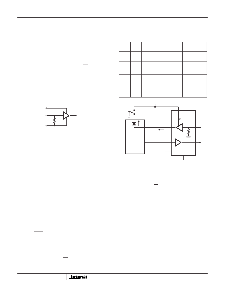
Receivers
The ISL83220E device contains a standard inverting
receiver that three-states via the EN control line. Receivers
convert RS-232 signals to CMOS output levels and accept
inputs up to
±
25V while presenting the required 3k
to 7k
input impedance (see Figure 1) even if the power is off
(V
CC
= 0V). The receiver's Schmitt trigger input stage uses
hysteresis to increase noise immunity and decrease errors
due to slow input signal transitions.
The ISL83220E receiver disables only when EN is driven
high. (see Table 2). This allows the receiver to monitor
external devices, like a modem, even when the ISL83220E is
in its 1
µ
A powerdown state.
Standard receivers driving powered down peripherals must
be disabled to prevent current flow through the peripheral's
protection diodes (see Figures 2). This renders them
useless for wake up functions.
Operation down to 2.7V
ISL83220E transmitter outputs meet RS-562 levels (
±
3.7V)
with V
CC
as low as 2.7V. RS-562 levels typically ensure inter
operability with RS-232 devices.
Powerdown Functionality
This 3V family of RS-232 interface devices requires a
nominal supply current of 0.3mA during normal operation
(not in powerdown mode), which is considerably less than
the 5mA to 11mA current required of 5V RS-232 devices.
The already low current requirement drops significantly
when the device enters powerdown mode. In powerdown,
supply current drops to 1
µ
A, because the on-chip charge
pump turns off (V+ collapses to V
CC
, V- collapses to GND),
and the transmitter outputs three-state. This micro-power
mode makes these devices ideal for battery powered and
portable applications.
Software Controlled (Manual) Powerdown
On the ISL83220E, the powerdown control is via a simple
shutdown (SHDN) pin. Driving this pin high enables normal
operation, while driving it low forces the IC into it's
powerdown state. Connect SHDN to V
CC
if the powerdown
function isn't needed. Note that the receiver output remains
enabled during shutdown (see Table 2). For the lowest
power consumption during powerdown, the receiver should
also be disabled by driving the EN input high (see next
section). The time to recover from manual powerdown mode
is typically 100
µ
s.
Receiver ENABLE Control
The ISL83220E also features an EN input to control the
receiver output. Driving EN high disables the receiver output
placing it in a high impedance state. This is useful to
eliminate supply current, due to a receiver output forward
biasing the protection diode, when driving the input of a
powered down (V
CC
= GND) peripheral (see Figure 2).
Capacitor Selection
The charge pumps require 0.1
µ
F capacitors for 3.3V
operation. Do not use values smaller than 0.1
µ
F. Increasing
the capacitor values (by a factor of 2) reduces ripple on the
transmitter outputs and slightly reduces power consumption.
When using minimum required capacitor values, make sure
that capacitor values do not degrade excessively with
temperature. If in doubt, use capacitors with a larger nominal
value. The capacitor's equivalent series resistance (ESR)
usually rises at low temperatures and it influences the
amount of ripple on V+ and V
-.
R
1OUT
GND
V
ROUT
V
CC
5k
R
1IN
-25V
V
RIN
+25V
GND
V
CC
FIGURE 1. INVERTING RECEIVER CONNECTIONS
TABLE 2. POWERDOWN AND ENABLE LOGIC TRUTH TABLE
SHDN
INPUT
EN
INPUT
TRANSMITTER
OUTPUT
RECEIVER
OUTPUT
MODE OF
OPERATION
L
L
High-Z
Active
Manual
Powerdown
L
H
High-Z
High-Z
Manual
Powerdown
w/Rcvr. Disabled
H
L
Active
Active
Normal
Operation
H
H
Active
High-Z
Normal
Operation
w/Rcvr. Disabled
FIGURE 2. POWER DRAIN THROUGH POWERED DOWN
PERIPHERAL
OLD
V
CC
POWERED
GND
SHDN = GND
V
CC
Rx
Tx
V
CC
CURRENT
V
OUT
=
V
CC
FLOW
RS-232 CHIP
DOWN
UART
ISL83220E