1
Æ
FN6047.3
ISL84051, ISL84052, ISL84053
Low-Voltage, Single and Dual Supply, 8 to
1 Multiplexer, Dual 4 to 1 Multiplexer and a
Triple SPDT Analog Switches
The Intersil ISL84051, ISL84052, ISL84053 devices are
precision, bidirectional, analog switches configured as a 8
channel multiplexer/demultiplexer (ISL84051), a dual
differential 4 channel multiplexer/demultiplexer (ISL84052)
and a triple single pole/double throw (SPDT) switch
(ISL84053) designed to operate from a single +2V to +12V
supply or from a
±
2V to
±
6V supply. All devices have an inhibit
pin to simultaneously open all signal paths.
ON resistance is 60
with a
±
5V supply and 125
with a
single +5V supply. Each switch can handle rail to rail analog
signals. The off-leakage current is only 0.1nA at +25
o
C or
5nA at +85
o
C with a ±5V supply.
All digital inputs have 0.8V to 2.4V logic thresholds, ensuring
TTL/CMOS logic compatibility when using a single +3.3V
and +5V supply or dual
±
5V supplies.
The ISL84051 is a 8 to 1 multiplexer device. The ISL84052 is
a dual 4 to 1 multiplexer device. The ISL84053 is a committed
triple SPDT, which is perfect for use in 2-to-1 multiplexer
applications.
Table 1 summarizes the performance of this family.
Related Literature
∑ Technical Brief TB363 "Guidelines for Handling and
Processing Moisture Sensitive Surface Mount Devices
(SMDs)"
∑ Application Note AN557 "Recommended Test Procedures
for Analog Switches"
Features
∑ Drop-in Replacements for MAX4051/A, MAX4052/A and
MAX4053/A
∑ Pin Compatible with MAX4581, MAX4582, MAX4583 and
with Industry Standard 74HC4051, 74HC4052 and
74HC4053
∑ ON Resistance (R
ON
) Max, V
S
=
±
5V . . . . . . . . . . . 100
∑ ON Resistance (R
ON
) Max, V
S
= +3V . . . . . . . . . . . 525
∑ R
ON
Matching Between Channels . . . . . . . . . . . . . . . . . <6
∑ Low Charge Injection . . . . . . . . . . . . . . . . . . . . . 10pC (Max)
∑ Single Supply Operation. . . . . . . . . . . . . . . . . . . +2V to +12V
∑ Dual Supply Operation . . . . . . . . . . . . . . . . . . . . . .
±
2V to
±
6
∑ Fast Switching Action (V
S
= +5V)
- t
ON
. . . . . . . . . . . . . . . . . . . . . . . . . . . . . . . . . . . . 90ns
- t
OFF
. . . . . . . . . . . . . . . . . . . . . . . . . . . . . . . . . . . 60ns
∑ Guaranteed Max Off-leakage @ V
S
=
±
5V. . . . . . . . . . 5nA
∑ Guaranteed Break-Before-Make
∑ TTL, CMOS Compatible
Applications
∑ Portable Equipment
∑ Communications Systems
- Radios
- Telecom Infrastructure
- ADSL, VDSL Modems
∑ Test Equipment
- Medical Ultrasound
- Magnetic Resonance Image
- CT and PET Scanners (MRI)
- ATE
- Electrocardiograph
∑ Audio and Video Signal Routing
∑ Various Circuits
- +3V/+5V DACs and ADCs
- Sample and Hold Circuits
- Operational Amplifier Gain Switching Networks
- High Frequency Analog Switching
- High Speed Multiplexing
- Integrator Reset Circuits
TABLE 1. FEATURES AT A GLANCE
CONFIGURATION
ISL84051
ISL84052
ISL84053
8:1 Mux
DUAL
4:1 Mux
TRIPLE
SPDT
±
5V R
ON
60
60
60
±
5V t
ON
/t
OFF
50ns/40ns
50ns/40ns
50ns/40ns
5V R
ON
125
125
125
5V t
ON
/t
OFF
90ns/60ns
90ns/60ns
90ns/60ns
3V R
ON
250
250
250
3V t
ON
/t
OFF
180ns/100ns
180ns/100ns
180ns/100ns
Packages
16 Ld SOIC, 16 Ld SSOP
Data Sheet
November 2003
CAUTION: These devices are sensitive to electrostatic discharge; follow proper IC Handling Procedures.
1-888-INTERSIL or 321-724-7143
|
Intersil (and design) is a registered trademark of Intersil Americas Inc.
Copyright © Intersil Americas Inc. 2003. All Rights Reserved.
All other trademarks mentioned are the property of their respective owners.
2
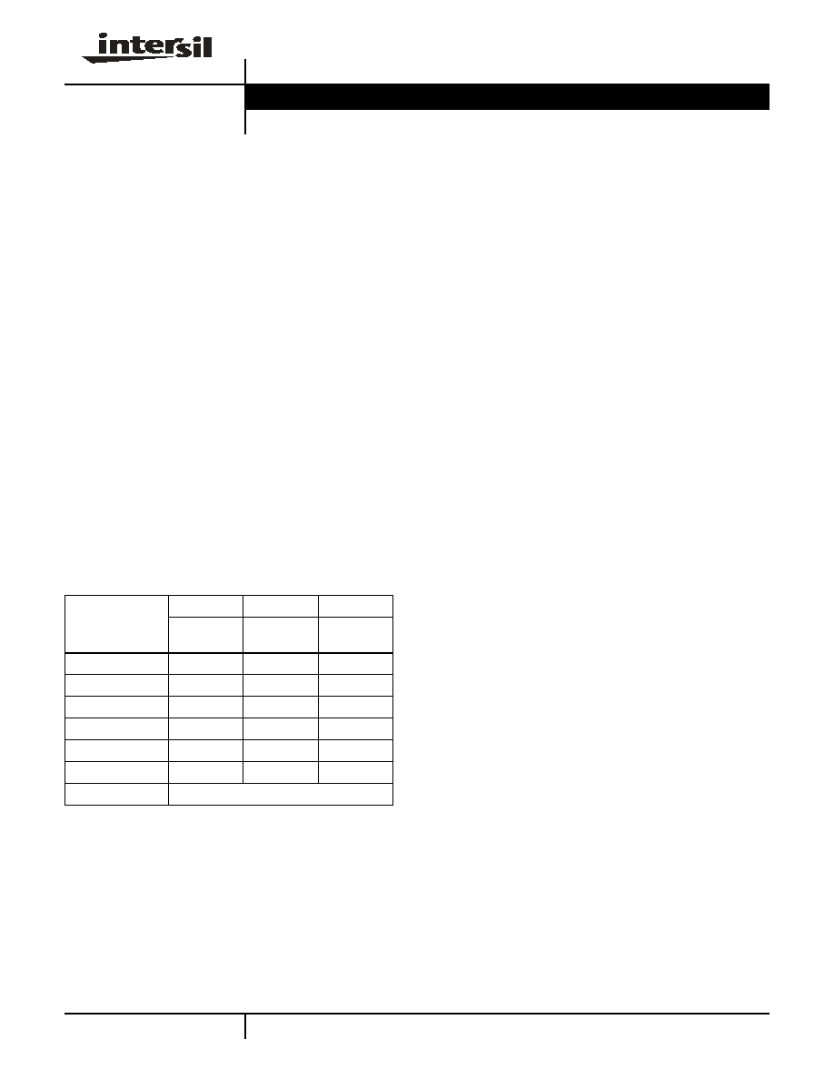
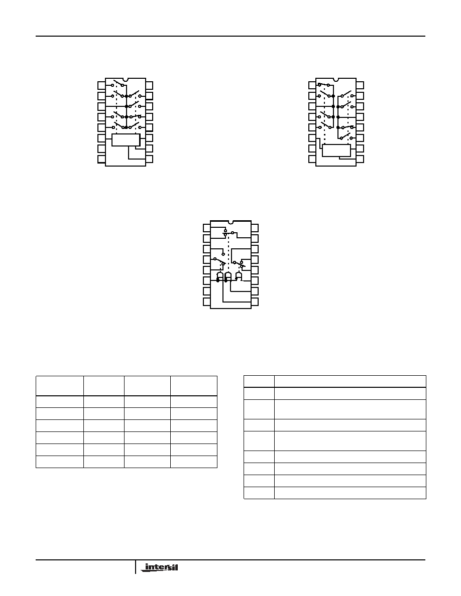
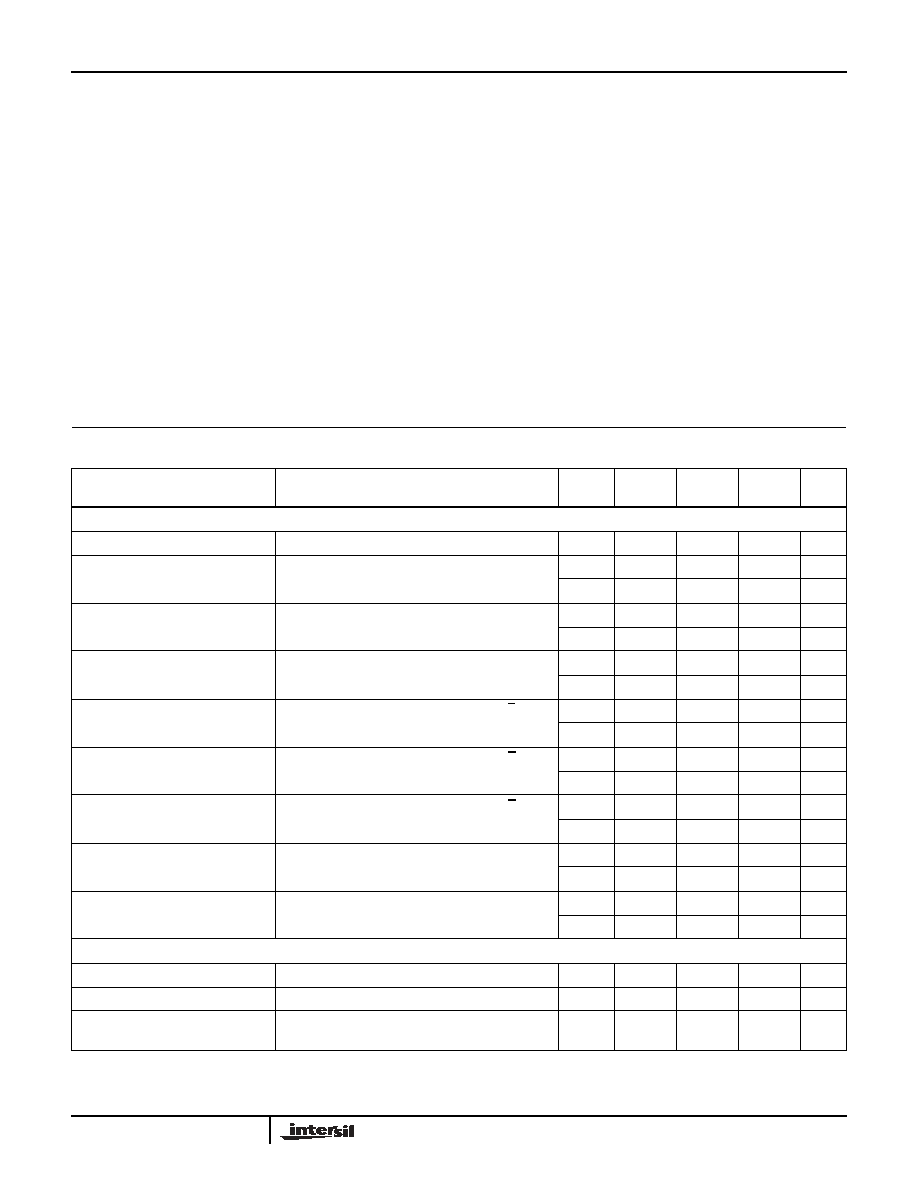
Pinouts
ISL84051 (SOIC, SSOP)
TOP VIEW
ISL84052 (SOIC, SSOP)
TOP VIEW
ISL84053 (SOIC, SSOP)
TOP VIEW
NOTE:
1. Switches Shown for Logic "0" Inputs.
14
15
16
9
13
12
11
10
1
2
3
4
5
7
6
8
NO1
NO3
COM
NO7
NO5
INH
GND
V-
V+
NO4
NO0
NO6
ADDC
ADDB
ADDA
NO2
LOGIC
14
15
16
9
13
12
11
10
1
2
3
4
5
7
6
8
NO0
B
NO1
B
COM
B
NO3
B
NO2
B
INH
GND
V-
V+
NO2
A
COM
A
NO0
A
NO3
A
ADDB
ADDA
NO1
A
LOGIC
14
15
16
9
13
12
11
10
1
2
3
4
5
7
6
8
NO
B
NC
B
NO
A
COM
A
NC
A
INH
GND
V-
V+
COM
C
NO
C
NC
C
ADD
C
ADD
B
ADD
A
COM
B
Ordering Information
PART NO.
TEMP.
RANGE (
o
C)
PACKAGE
PKG. DWG. #
ISL84051IB
-40 to 85
16 Ld SOIC
M16.15
ISL84051IA
-40 to 85
16 Ld SSOP
M16.15A
ISL84052IB
-40 to 85
16 Ld SOIC
M16.15
ISL84052IA
-40 to 85
16 Ld SSOP
M16.15A
ISL84053IB
-40 to 85
16 Ld SOIC
M16.15
ISL84053IA
-40 to 85
16 Ld SSOP
M16.15A
NOTE: Most surface mount devices are available on tape and reel;
add "-T" to suffix.
Pin Description
PIN
FUNCTION
V+
Positive Power Supply Input
V-
Negative Power Supply Input. Connect to GND for
Single Supply Configurations.
GND
Ground Connection
INH
Digital Control Input. Connect to GND for Normal
Operation. Connect to V+ to turn all switches off.
COM
Analog Switch Common Pin
NO
Analog Switch Normally Open Pin
NC
Analog Switch Normally Closed Pin
ADD
Address Input Pin
ISL84051, ISL84052, ISL84053

3
Truth Tables
ISL84051
INH
ADDC
ADDB
ADDA
SWITCH
ON
1
X
X
X
None
0
0
0
0
NO0
0
0
0
1
NO1
0
0
1
0
NO2
0
0
1
1
NO3
0
1
0
0
NO4
0
1
0
1
NO5
0
1
1
0
NO6
0
1
1
1
NO7
ISL84052
INH
ADDB
ADDA
SWITCH ON
1
X
X
None
0
0
0
NO0
0
0
1
NO1
0
1
0
NO2
0
1
1
NO3
ISL84053
INH
ADD
C
ADD
B
ADD
A
SWITCH ON
1
X
X
X
None
0
X
X
0
NC
A
0
X
X
1
NO
A
0
X
0
X
NC
B
0
X
1
X
NO
B
0
0
X
X
NC
C
0
1
X
X
NO
C
NOTE: Logic "0"
0.8V. Logic "1"
2.4V, with V+ between 2.7V and
10V. X = Don't Care.
ISL84051, ISL84052, ISL84053
4
Absolute Maximum Ratings
Thermal Information
V+ to V- . . . . . . . . . . . . . . . . . . . . . . . . . . . . . . . . . . . . . . -0.3 to15V
V+ to GND . . . . . . . . . . . . . . . . . . . . . . . . . . . . . . . . . . . . -0.3 to15V
V- to GND . . . . . . . . . . . . . . . . . . . . . . . . . . . . . . . . . . . -15 to 0.3V
Input Voltages
INH, NO, NC, ADD (Note 2) . . . . . . . . . ((V-)-0.3) to ((V+) + 0.3V)
Output Voltages
COM (Note 2) . . . . . . . . . . . . . . . . . . . . ((V-)-0.3) to ((V+) + 0.3V)
Continuous Current (Any Terminal) . . . . . . . . . . . . . . . . . . . .
±
30mA
Peak Current NO, NC, or COM
(Pulsed 1ms, 10% Duty Cycle, Max) . . . . . . . . . . . . . . . . . .
±
100mA
ESD Rating
HBM (Per MIL-STD-883, Method 3015.7) . . . . . . . . . . . . . . >2kV
Thermal Resistance (Typical, Note 3)
JA
(
o
C/W)
16 Ld SOIC Package . . . . . . . . . . . . . . . . . . . . . . . .
115
16 Ld SSOP Package . . . . . . . . . . . . . . . . . . . . . . .
160
Maximum Junction Temperature (Plastic Package) . . . . . . . 150
o
C
Maximum Storage Temperature Range. . . . . . . . . . . . -65
o
C to 150
o
C
Maximum Lead Temperature (Soldering 10s) . . . . . . . . . . . . 300
o
C
(Lead Tips Only)
Operating Conditions
Temperature Range
ISL8405XIX . . . . . . . . . . . . . . . . . . . . . . . . . . . . . . . . -40
o
C to 85
o
C
CAUTION: Stresses above those listed in "Absolute Maximum Ratings" may cause permanent damage to the device. This is a stress only rating and operation of the
device at these or any other conditions above those indicated in the operational sections of this specification is not implied.
NOTES:
2. Signals on NC, NO, COM, ADD, or INH exceeding V+ or V- are clamped by internal diodes. Limit forward diode current to maximum current
ratings.
3.
JA
is measured with the component mounted on a low effective thermal conductivity test board in free air. See Tech Brief TB379 for details.
Electrical Specifications:
±
5V Supply
Test Conditions: V
SUPPLY
=
±
4.5V to
±
5.5V, GND = 0V, V
INH
= 2.4V, V
INL
= 0.8V (Note 4),
Unless Otherwise Specified
PARAMETER
TEST CONDITIONS
TEMP
(
o
C)
(NOTE 5)
MIN
TYP
(NOTE 5)
MAX
UNITS
ANALOG SWITCH CHARACTERISTICS
Analog Signal Range, V
ANALOG
Full
V-
-
V+
V
ON Resistance, R
ON
V
S
=
±
5V, I
COM
= 1mA, V
NO
or V
NC
=
±
3V,
(See Figure 5)
25
-
60
100
Full
-
-
125
R
ON
Matching Between Channels,
R
ON
V
S
=
±
5V, I
COM
= 1mA, V
NO
or V
NC
=
±
3V, (Note 6)
25
-
-
6
Full
-
-
12
R
ON
Flatness, R
FLAT(ON)
V
S
=
±
5V, I
COM
= 1mA, V
NO
or V
NC
=
±
3V, 0V,
(Note 7)
25
-
-
10
Full
-
-
15
NO or NC OFF Leakage Current,
I
NO(OFF)
or I
NC(OFF)
V
S
=
±
5.5V, V
COM
=
±
4.5V, V
NO
or V
NC
= +4.5V,
(Note 8)
25
-0.1
0.002
0.1
nA
Full
-5
-
5
nA
COM OFF Leakage Current,
I
COM(OFF)
, (ISL84051)
V
S
=
±
5.5V, V
COM
=
±
4.5V, V
NO
or V
NC
= +4.5V,
(Note 8)
25
-0.1
0.002
0.1
nA
Full
-5
-
5
nA
COM OFF Leakage Current,
I
COM(OFF)
, (ISL84052, ISL84053)
V
S
=
±
5.5V, V
COM
=
±
4.5V, V
NO
or V
NC
= +4.5V,
(Note 8)
25
-0.1
0.002
0.1
nA
Full
-2.5
-
2.5
nA
COM ON Leakage Current,
I
COM(ON)
, (ISL84051)
V
S
=
±
5.5V, V
COM
= V
NO
or V
NC
=
±
4.5V,
(Note 8)
25
-0.1
0.002
0.1
nA
Full
-5
-
5
nA
COM ON Leakage Current,
I
COM(ON)
, (ISL84052, ISL84053)
V
S
=
±
5.5V, V
COM
= V
NO
or V
NC
=
±
4.5V, (Note 8)
25
-0.1
0.002
0.1
nA
Full
-2.5
-
2.5
nA
DIGITAL INPUT CHARACTERISTICS
Input Voltage High, V
INH
, V
ADDH
Full
2.4
-
-
V
Input Voltage Low, V
INL
, V
ADDL
Full
-
-
0.8
V
Input Current, I
INH
, I
INL
, I
ADDH
,
I
ADDL
V
S
=
±
5.5V, V
INH
, V
ADD
= 0V or V+
Full
-1
0.03
1
µ
A
ISL84051, ISL84052, ISL84053

5
DYNAMIC CHARACTERISTICS
Inhibit Turn-ON Time, t
ON
V
S
=
±
4.5V, V
NO
or V
NC
=
±
3V, R
L
= 300
,
C
L
= 35pF, V
IN
= 0 to 3, (See Figure 1)
25
-
50
175
ns
Full
-
-
225
ns
Inhibit Turn-OFF Time, t
OFF
V
S
=
±
4.5V, V
NO
or V
NC
=
±
3V, R
L
= 300
,
C
L
= 35pF, V
IN
= 0 to 3, (See Figure 1)
25
-
40
150
ns
Full
-
-
200
ns
Address Transition Time, t
TRANS
V
S
=
±
4.5V, V
NO
or V
NC
=
±
3V, R
L
= 300
,
C
L
= 35pF, V
IN
= 0 to 3, (See Figure 1)
25
-
75
250
ns
Break-Before-Make Time, t
BBM
V
S
=
±
5.5V, V
NO
or V
NC
= 3V, R
L
= 300
,
C
L
= 35pF, V
IN
= 0 to 3V, (See Figure 3)
25
2
10
-
ns
Charge Injection, Q
C
L
= 1.0nF, V
G
= 0V, R
G
= 0
, (See Figure 2)
25
-
2
10
pC
NO/NC OFF Capacitance, C
OFF
f = 1MHz, V
NO
or V
NC
= V
COM
= 0V, (See Figure 7)
25
-
3
-
pF
COM OFF Capacitance, C
OFF
f = 1MHz, V
NO
or V
NC
= V
COM
= 0V,
(See Figure 7)
ISL84051
25
-
21
-
pF
ISL84052
25
-
12
-
pF
ISL84053
25
-
9
-
pF
COM ON Capacitance, C
COM(ON)
f = 1MHz, V
NO
or V
NC
= V
COM
= 0V,
(See Figure 7)
ISL84051
25
-
26
-
pF
ISL84052
25
-
18
-
pF
ISL84053
25
-
14
-
pF
OFF Isolation
R
L
= 50
, C
L
= 15pF, f = 100kHz,
V
NO
or V
NC
= 1V
RMS
, (See Figures 4 and 6)
25
-
<90
-
dB
Crosstalk, (Note 9) (ISL84052,
ISL84053 only)
25
-
<-90
-
dB
POWER SUPPLY CHARACTERISTICS
Power Supply Range
Full
±
2
-
±
6
V
Positive Supply Current, I+
V
S
=
±
5.5V, V
INH
, V
ADD
= 0V or V+, Switch On or
Off
25
-1
0.1
1
µ
A
Full
-10
-
10
µ
A
Negative Supply Current, I-
25
-1
0.1
1
µ
A
Full
-10
-
10
µ
A
NOTES:
4. V
IN
= Input voltage to perform proper function.
5. The algebraic convention, whereby the most negative value is a minimum and the most positive a maximum, is used in this data sheet.
6.
R
ON
= R
ON
(MAX) - R
ON
(MIN).
7. Flatness is defined as the difference between maximum and minimum value of on-resistance over the specified analog signal range.
8. Leakage parameter is 100% tested at high temp, and guaranteed by correlation at 25
o
C.
9. Between any two switches.
Electrical Specifications:
±
5V Supply
Test Conditions: V
SUPPLY
=
±
4.5V to
±
5.5V, GND = 0V, V
INH
= 2.4V, V
INL
= 0.8V (Note 4),
Unless Otherwise Specified (Continued)
PARAMETER
TEST CONDITIONS
TEMP
(
o
C)
(NOTE 5)
MIN
TYP
(NOTE 5)
MAX
UNITS
ISL84051, ISL84052, ISL84053