
1
Æ
FN6025.3
ISL84514, ISL84515
Low-Voltage, Single Supply, SPST,
Analog Switches
The Intersil ISL84514 and ISL84515 devices are precision,
analog switches designed to operate from a single +2.4V to
+12V supply. Targeted applications include battery powered
equipment that benefit from the devices' low power
consumption (5
µ
W), and low leakage currents (1nA). Low
R
ON
and fast switching speeds over a wide operating supply
range make these switches ideal for use in industrial
equipment, portable instruments, and as input signal
multiplexers for new generation, low supply voltage data
converters. Some of the smallest packages available alleviate
board space limitations, and make Intersil's newest line of
low-voltage switches an ideal solution for space constrained
products.
The ISL8451X are single-pole/single-throw (SPST) switches,
with the ISL84514 being normally open (NO), and the
ISL84515 being normally closed (NC).
Table 1 summarizes the performance of this family. For higher
performance, pin compatible versions, see the ISL43110,
ISL43111 data sheet. For
±
5V supply versions, see the
ISL84516, ISL84517 data sheet.
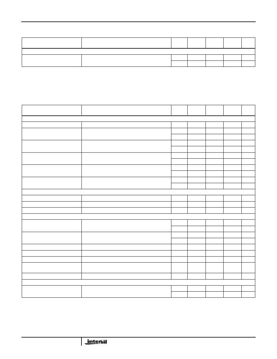
TABLE 1. FEATURES AT A GLANCE
Related Literature
∑ Technical Brief TB363 "Guidelines for Handling and
Processing Moisture Sensitive Surface Mount Devices
(SMDs)"
∑ Application Note AN557 "Recommended Test Procedures
for Analog Switches"
Features
∑ Drop-in Replacements for MAX4514 and MAX4515
∑ Available in SOT-23 Packaging
∑ Fully Specified for 5V and 12V Supplies
∑ Single Supply Operation. . . . . . . . . . . . . . . . . +2.4V to +12V
∑ ON Resistance (R
ON
Max). . . . . . . . . . . . . 20
(V+ = 5V)
10
(V+ = 12V)
∑ R
ON
Flatness (Max) . . . . . . . . . . . . . . . . . . . . . . . . . . . . . . 3
∑ Charge Injection (Max) . . . . . . . . . . . . . . . . . . . . . . . . . . 10pC
∑ Low Power Consumption (P
D
) . . . . . . . . . . . . . . . . . . . .<5
µ
W
∑ Low Leakage Current (Max at 85
o
C) . 20nA (Off Leakage)
40nA (On Leakage)
∑ Fast Switching Action
- t
ON
(Max) . . . . . . . . . . . . . . . . . . . . . . . . . . . . . . 150ns
- t
OFF
(Max) . . . . . . . . . . . . . . . . . . . . . . . . . . . . . 100ns
∑ Minimum 2000V ESD Protection per Method 3015.7
∑ TTL, CMOS Compatible
Applications
∑ Battery Powered, Handheld, and Portable Equipment
∑ Communications Systems
- Radios
- Telecom Infrustructure
∑ Test Equipment
- Logic and Spectrum Analyzers
- Portable Meters
∑ Medical Equipment
- Ultrasound and MRI
- Electrocardiograph
∑ Audio and Video Switching
∑ General Purpose Circuits
- +3V/+5V DACs and ADCs
- Sample and Hold Circuits
- Digital Filters
- Operational Amplifier Gain Switching Networks
- High Frequency Analog Switching
- High Speed Multiplexing
- Integrator Reset Circuits
ISL84514
ISL84515
Number of Switches
1
1
Configuration
NO
NC
3.3V R
ON
20
20
3.3V t
ON
/t
OFF
60ns/30ns
60ns/30ns
5V R
ON
12
12
5V t
ON
/t
OFF
45ns/25ns
45ns/25ns
12V R
ON
8
8
12V t
ON
/t
OFF
40ns/25ns
40ns/25ns
Packages
8 Ld SOIC, 5 Ld SOT-23
Data Sheet
June 2003
CAUTION: These devices are sensitive to electrostatic discharge; follow proper IC Handling Procedures.
1-888-INTERSIL or 321-724-7143
|
Intersil (and design) is a registered trademark of Intersil Americas Inc.
Copyright © Intersil Americas Inc. 2003. All Rights Reserved.
All other trademarks mentioned are the property of their respective owners.

2
Truth Table
Pin Description
Ordering Information
Pinouts
(Note 1)
ISL84514 (SOIC)
TOP VIEW
ISL84514 (SOT-23)
TOP VIEW
ISL84515 (SOIC)
TOP VIEW
ISL84515 (SOT-23)
TOP VIEW
NOTE:
1. Switches Shown for Logic "0" Input.
COM
GND
V+
NO
IN
6
7
8
5
1
2
3
4
N.C.
N.C.
N.C.
4
5
1
2
3
COM
V+
GND
NO
IN
COM
GND
V+
NC
IN
6
7
8
5
1
2
3
4
N.C.
N.C.
N.C.
4
5
1
2
3
COM
V+
GND
NC
IN
LOGIC
ISL84514
ISL84515
0
OFF
ON
1
ON
OFF
NOTE: Logic "0"
0.8V. Logic "1"
2.4V.
PIN
FUNCTION
V+
System Power Supply Input (+2.4V to +12V)
GND
Ground Connection
IN
Digital Control Input
COM
Analog Switch Common Pin
NO
Analog Switch Normally Open Pin
NC
Analog Switch Normally Closed Pin
N.C.
No Internal Connection
PART NO.
(BRAND)
TEMP.
RANGE
(
o
C)
PACKAGE
PKG. DWG. #
ISL84514IB
-40 to 85
8 Ld SOIC
M8.15
ISL84514IB-T
-40 to 85
8 Ld SOIC
Tape and Reel
M8.15
ISL84514IH-T
(514I)
-40 to 85
5 Ld SOT-23,
Tape and Reel
P5.064
ISL84515IB
-40 to 85
8 Ld SOIC
M8.15
ISL84515IB-T
-40 to 85
8 Ld SOIC
Tape and Reel
M8.15
ISL84515IH-T
(515I)
-40 to 85
5 Ld SOT-23,
Tape and Reel
P5.064
ISL84514, ISL84515

3
Absolute Maximum Ratings
Thermal Information
V+ to GND . . . . . . . . . . . . . . . . . . . . . . . . . . . . . . . . . . . . -0.3 to15V
Input Voltages
IN (Note 2) . . . . . . . . . . . . . . . . . . . . . . . . . . . . -0.3 to ((V+) + 0.3V)
NO, NC (Note 2) . . . . . . . . . . . . . . . . . . . . . . . -0.3 to ((V+) + 0.3V)
Output Voltages
COM (Note 2). . . . . . . . . . . . . . . . . . . . . . . . . . -0.3 to ((V+) + 0.3V)
Continuous Current (Any Terminal) . . . . . . . . . . . . . . . . . . . . . 20mA
Peak Current NO, NC, or COM
(Pulsed 1ms, 10% Duty Cycle, Max) . . . . . . . . . . . . . . . . . . . . 30mA
ESD Rating (Per MIL-STD-883 Method 3015). . . . . . . . . . . . . >2kV
Operating Conditions
Temperature Range
ISL8451XIX . . . . . . . . . . . . . . . . . . . . . . . . . . . . . . . . -40
o
C to 85
o
C
Thermal Resistance (Typical, Note 3)
JA
(
o
C/W)
5 Ld SOT-23 Package . . . . . . . . . . . . . . . . . . . . . . .
225
8 Ld SOIC Package . . . . . . . . . . . . . . . . . . . . . . . . .
170
Maximum Junction Temperature (Plastic Package) . . . . . . . 150
o
C
Moisture Sensitivity (See Technical Brief TB363)
All Packages . . . . . . . . . . . . . . . . . . . . . . . . . . . . . . . . . . . Level 1
Maximum Storage Temperature Range. . . . . . . . . . . . -65
o
C to 150
o
C
Maximum Lead Temperature (Soldering 10s) . . . . . . . . . . . . 300
o
C
(Lead Tips Only)
CAUTION: Stresses above those listed in "Absolute Maximum Ratings" may cause permanent damage to the device. This is a stress only rating and operation of the
device at these or any other conditions above those indicated in the operational sections of this specification is not implied.
NOTES:
2. Signals on NO, NC, COM, or IN exceeding V+ or GND are clamped by internal diodes. Limit forward diode current to maximum current ratings.
3.
JA
is measured with the component mounted on a low effective thermal conductivity test board in free air. See Tech Brief TB379 for details.
Electrical Specifications
Test Conditions: V+ = +4.5V to +5.5V, GND = 0V, V
INH
= 2.4V, V
INL
= 0.8V (Note 4),
Unless Otherwise Specified
PARAMETER
TEST CONDITIONS
TEMP
(
o
C)
(NOTE 5)
MIN
TYP
(NOTE 5)
MAX
UNITS
ANALOG SWITCH CHARACTERISTICS
Analog Signal Range, V
ANALOG
Full
0
-
V+
V
ON Resistance, R
ON
V+ = 4.5V, I
COM
= 1.0mA, V
COM
= 3.5V,
(See Figure 4)
25
-
-
20
Full
-
-
25
R
ON
Flatness, R
FLAT(ON)
V+ = 4.5V, I
COM
= 1.0mA, V
COM
= 1V, 2V, 3V
25
-
-
3
Full
-
-
5
NO or NC OFF Leakage Current,
I
NO(OFF)
or I
NC(OFF)
V+ = 5.5V, V
COM
= 1V, 4.5V, V
NO
or V
NC
= 4.5V, 1V,
(Note 6)
25
-1
0.01
1
nA
Full
-20
-
20
nA
COM OFF Leakage Current,
I
COM(OFF)
V+ = 5.5V, V
COM
= 4.5V, 1V, V
NO
or V
NC
= 1V, 4.5V,
(Note 6)
25
-1
0.01
1
nA
Full
-20
-
20
nA
COM ON Leakage Current,
I
COM(ON)
V
+
= 5.5V, V
COM
= 1V, 4.5V, or V
NO
or V
NC
= 1V,
4.5V, (Note 6)
25
-2
0.01
2
nA
Full
-40
-
40
nA
DIGITAL INPUT CHARACTERISTICS
Input Voltage High, V
INH
Full
2.4
-
V+
V
Input Voltage Low, V
INL
Full
0
-
0.8
V
Input Current, I
INH
, I
INL
V+ = 5.5V, V
IN
= 0V or V+
Full
-1
-
1
µ
A
DYNAMIC CHARACTERISTICS
Turn-ON Time, t
ON
V
NO
or V
NC
= 3V, R
L
= 300
, C
L
= 35pF,
V
IN
= 0 to 3V, (See Figure 1)
25
-
-
150
ns
Full
-
-
240
ns
Turn-OFF Time, t
OFF
V
NO
or V
NC
= 3V, R
L
= 300
, C
L
= 35pF,
V
IN
= 0 to 3V, (See Figure 1)
25
-
-
100
ns
Full
-
-
150
ns
Charge Injection, Q
C
L
= 1.0nF, V
G
= 0V, R
G
= 0
, (See Figure 2)
25
-
2
10
pC
OFF Isolation
R
L
= 50
, C
L
= 15pF, f = 100kHz, (See Figure 3)
25
-
>90
-
dB
NO or NC OFF Capacitance, C
OFF
f = 1MHz, V
NO
or V
NC
= V
COM
= 0V, (See Figure 5)
25
-
14
-
pF
COM OFF Capacitance,
C
COM(OFF)
f = 1MHz, V
NO
or V
NC
= V
COM
= 0V, (See Figure 5)
25
-
14
-
pF
COM ON Capacitance, C
COM(ON)
f = 1MHz, V
NO
or V
NC
= V
COM
= 0V, (See Figure 5)
25
-
30
-
pF
ISL84514, ISL84515
4
POWER SUPPLY CHARACTERISTICS
Positive Supply Current, I+
V+ = 5.5V, V
IN
= 0V or V+, Switch On or Off
25
-1
0.0001
1
µ
A
Full
-10
-
10
µ
A
NOTES:
4. V
IN
= input voltage to perform proper function.
5. The algebraic convention, whereby the most negative value is a minimum and the most positive a maximum, is used in this data sheet.
6. Leakage parameter is 100% tested at high temp, and guaranteed by correlation at 25
o
C.
Electrical Specifications - 12V Supply
Test Conditions: V+ = +10.8V to +13.2V, GND = 0V, V
INH
= 5V, V
INL
= 0.8V (Note 4),
Unless Otherwise Specified
PARAMETER
TEST CONDITIONS
TEMP
(
o
C)
(NOTE 5)
MIN
TYP
(NOTE 5)
MAX
UNITS
ANALOG SWITCH CHARACTERISTICS
Analog Signal Range, V
ANALOG
Full
0
-
V+
V
ON Resistance, R
ON
V+ = 10.8V, I
COM
= 1.0mA, V
COM
= 10V
25
-
-
10
Full
-
-
15
R
ON
Flatness, R
FLAT(ON)
V+ = 12V, I
COM
= 1.0mA, V
COM
= 3V, 6V, 9V
25
-
-
3
Full
-
-
5
NO or NC OFF Leakage Current,
I
NO(OFF)
or I
NC(OFF)
V+ = 13.2V, V
COM
= 1V, 10V, V
NO
or V
NC
= 10V, 1V,
(Note 6)
25
-2
-
2
nA
Full
-50
-
50
nA
COM OFF Leakage Current,
I
COM(OFF)
V+ = 13.2V, V
COM
= 10V, 1V, V
NO
or V
NC
= 1V, 10V,
(Note 6)
25
-2
-
2
nA
Full
-50
-
50
nA
COM ON Leakage Current,
I
COM(ON)
V+ = 13.2V, V
COM
= 1V, 10V, or V
NO
or V
NC
= 1V,
10V, (Note 6)
25
-4
-
4
nA
Full
-100
-
100
nA
DIGITAL INPUT CHARACTERISTICS
Input Voltage High, V
INH
Full
5
3
V+
V
Input Voltage Low, V
INL
Full
0
-
0.8
V
Input Current, I
INH
, I
INL
V+ = 13.2V, V
IN
= 0V or V+
Full
-1
-
1
µ
A
DYNAMIC CHARACTERISTICS
Turn-ON Time, t
ON
V
NO
or V
NC
= 10V, R
L
= 300
, C
L
= 35pF,
V
IN
= 0 to 5V, (See Figure 1)
25
-
-
150
ns
Full
-
-
240
ns
Turn-OFF Time, t
OFF
V
NO
or V
NC
= 10V, R
L
= 300
, C
L
= 35pF,
V
IN
= 0 to 5V, (See Figure 1)
25
-
-
100
ns
Full
-
-
150
ns
Charge Injection, Q
C
L
= 1.0nF, V
G
= 0V, R
G
= 0
, (See Figure 2)
25
-
8
20
pC
OFF Isolation
R
L
= 50
, C
L
= 15pF, f = 100kHz, (See Figure 3)
25
-
>90
-
dB
NO or NC OFF Capacitance, C
OFF
f = 1MHz, V
NO
or V
NC
= V
COM
= 0V, (See Figure 5)
25
-
14
-
pF
COM OFF Capacitance,
C
COM(OFF)
f = 1MHz, V
NO
or V
NC
= V
COM
= 0V, (See Figure 5)
25
-
14
-
pF
COM ON Capacitance, C
COM(ON)
f = 1MHz, V
NO
or V
NC
= V
COM
= 0V, (See Figure 5)
25
-
30
-
pF
POWER SUPPLY CHARACTERISTICS
Positive Supply Current, I+
V+ = 13.2V, V
IN
= 0V or V+, Switch On or Off
25
-2
-
2
µ
A
Full
-20
-
20
µ
A
Electrical Specifications
Test Conditions: V+ = +4.5V to +5.5V, GND = 0V, V
INH
= 2.4V, V
INL
= 0.8V (Note 4),
Unless Otherwise Specified (Continued)
PARAMETER
TEST CONDITIONS
TEMP
(
o
C)
(NOTE 5)
MIN
TYP
(NOTE 5)
MAX
UNITS
ISL84514, ISL84515

5
Electrical Specifications - 3.3V Supply
Test Conditions: V+ = +3.0V to +3.6V, GND = 0V, V
INH
= 2.4V, V
INL
= 0.8V (Note 4),
Unless Otherwise Specified
PARAMETER
TEST CONDITIONS
TEMP
(
o
C)
(NOTE 5)
MIN
TYP
(NOTE 5)
MAX
UNITS
ANALOG SWITCH CHARACTERISTICS
Analog Signal Range, V
ANALOG
Full
0
-
V+
V
ON Resistance, R
ON
V+ = 3V, I
COM
= 1.0mA, V
COM
= 1.5V
25
-
-
50
Full
-
-
75
R
ON
Flatness, R
FLAT(ON)
I
COM
= 1.0mA, V
COM
= 0.5V, 1V, 1.5V
25
-
-
5.5
Full
-
-
7.0
NO or NC OFF Leakage Current,
I
NO(OFF)
or I
NC(OFF)
V+ = 3.6V, V
COM
= 3V, 1V, V
NO
or V
NC
= 1V, 3V,
(Note 6)
25
-1
0.01
1
nA
Full
-20
-
20
nA
COM OFF Leakage Current,
I
COM(OFF)
V+ = 3.6V, V
COM
= 3V, 1V, V
NO
or V
NC
= 1V, 3V,
(Note 6)
25
-1
0.01
1
nA
Full
-20
-
20
nA
COM ON Leakage Current,
I
COM(ON)
V+ = 3.6V, V
COM
= 1V, 3V, or V
NO
or V
NC
= 1V, 3V,
(Note 6)
25
-2
0.01
2
nA
Full
-40
-
40
nA
DIGITAL INPUT CHARACTERISTICS
Input Voltage High, V
INH
Full
2.4
-
V+
V
Input Voltage Low, V
INL
Full
0
-
0.8
V
Input Current, I
INH
, I
INL
V+ = 3.6V, V
IN
= 0V or V+
Full
-1
-
1
µ
A
DYNAMIC CHARACTERISTICS
Turn-ON Time, t
ON
V
NO
or V
NC
= 1.5V, R
L
= 300
, C
L
= 35pF,
V
IN
= 0 to 3V
25
-
-
150
ns
Full
-
-
240
ns
Turn-OFF Time, t
OFF
V
NO
or V
NC
= 1.5V, R
L
= 300
, C
L
= 35pF,
V
IN
= 0 to 3V
25
-
-
100
ns
Full
-
-
150
ns
Charge Injection, Q
C
L
= 1.0nF, V
G
= 0V, R
G
= 0
25
-
4
10
pC
POWER SUPPLY CHARACTERISTICS
Positive Supply Current, I+
V+ = 3.6V, V
IN
= 0V or V+, Switch On or Off
25
-1
-
1
µ
A
Full
-10
-
10
µ
A
Test Circuits and Waveforms
Logic input waveform is inverted for switches that have the opposite
logic sense.
FIGURE 1A. MEASUREMENT POINTS
C
L
includes fixture and stray capacitance.
FIGURE 1B. TEST CIRCUIT
FIGURE 1. SWITCHING TIMES
50%
t
r
< 20ns
t
f
< 20ns
t
OFF
90%
3V or 5V
0V
0V
t
ON
LOGIC
INPUT
SWITCH
INPUT
SWITCH
OUTPUT
90%
V
OUT
V
OUT
V(NO or NC)
R
L
R
L
R
ON
(
)
+
------------------------------
=
SWITCH
INPUT
LOGIC
INPUT
V
OUT
R
L
C
L
COM
NO or NC
IN
300
35pF
GND
V+
C
ISL84514, ISL84515